

Analog Microelectronics AME7107Y, AME7107RCPL, AME7107CPL, AME7107ACKW, AME7106Y Datasheet
...
AME, Inc.
AME7106/AME7106A/AME7106R
AME7107/AME7107A/AME7107R
nn
n Key Features
nn
l 100µV Resolution
l High Impedance Differential Inputs
l Differential Reference
l Drive LCD (AME7106) or LED (AME7107)
Directly
l Four New Convenient Features
(AME7106A/AME7107A)
l Display-Hold
l Low-Battery Indication
l Integration Status Indication
l De-Integration Status Indication
nn
n Applications
nn
l Digital multimeter
l pH meter
l Capacitance meter
l Thermometer
l Digital Panel meter
l Photometer
3-1/2 Digit A/D Converter
High Accuracy, Low Power
nn
n General Description
nn
The AME7106 and AME7107 family are high performance, low power, 3-1/2 digit, dual-slope integrating A/
D converters, with on-chip display drivers. The
AME7106 is designed for a single battery operated system, will drive non-multiplexed LCD display directly.
The AME7107 is designed for a dual power supply system, will directly drive common anode LED display.
These A/D converters are inherently versatile and accurate. They are immune to the high noise environments. The true differential high impedance inputs and
differential reference are very useful for making
ratiometric measurement, such as resistance, strain
gauge and bridge transducers. The built-in auto-zero
feature automatically corrects the system offset without any external adjustments.
Display-hold, low-battery flag, integration and de-integration status flags are four additional features which
are available in the 44-pin package, AME7106ACKW
and AME7107ACKW.
nn
n Typical Operating Circuit
nn
* For the operating circuit of the reverse-pins version, please refer
to pin configuration on page 4 and pin description on page 5 & 6
1
AME, Inc.
AME7106/AME7106A/AME7106R
AME7107/AME7107A/AME7107R
nn
n Absolute Maximum Ratings
nn
AME7106
Supply Voltage (V+ to V-) 12V
Analog Input Volt ag e (Either inputs) V+ TO VReference Input Vol tage (Eith er i np uts ) V+ TO VClock Input Test to V+
Power Di ssipation 800mW
Operat ing Tempera ture 0
Storage Temperature -55
Lead Temperature (S ol d eri ng 60 s e c ond s)
AME7107
Supply Voltage
V+ 6V
V- -6V
Analog Input Voltage (Either inputs) V+ to VReference Input Voltage (Either inputs) V+ to VClock Input Gnd to V+
Power Dissipati o n 800mW
Operating Temperature 0
Storage Temperature -55
Lead Temperatur e (Solder ing 60 seconds)
3-1/2 Digit A/D Converter
High Accuracy, Low Power
o
C to 70oC
o
C to 150oC
o
300
C
o
C to 70oC
o
C to 150oC
o
C
300
Static sensitive device. Unused devices must be stored in the conductive material.
Protect device from static discharge and static field. Stresses exceed the above Absolute Maximum
Ratings may cause permanent damage to the device. Exposure to Absolute Maximum Rating Conditions for extended periods may affect the reliability of the device.
2

AME, Inc.
AME7106/AME7106A/AME7106R
AME7107/AME7107A/AME7107R
nn
n Ordering Information
nn
Pa rt Numbe r Displa y Marki ng Pa cka ge Pin Layout Tem p. Ra nge
AME7106CPL LCD
AME7106RCPL LCD
AME7106ACKW LCD
AME7106Y LCD
AME7107CPL LED
AME7107RCPL LED
AME7107ACKW LED
AME7107Y LED
AME7106CPL
AME7106RCPL
AME7106ACKW
AME7107CPL
AME7107RCPL
AME7107ACKW
YYWW
YYWW
YYWW
AME7106Y
YYWW
YYWW
YYWW
YYWW
AME7107Y
YYWW
3-1/2 Digit A/D Converter
High Accuracy, Low Power
40 Pin P DIP Normal
40 Pin P DIP Reverse
44 Pin P Q F P Normal
44 Pin Di ce Normal
40 Pin P DIP Normal
40 Pin P DIP Reverse
44 Pin P Q F P Normal
44 Pin Di ce Normal
o
C to 70oC
0
o
0
C to 71oC
o
C to 72oC
0
o
0
C to 73oC
o
0
C to 74oC
o
C to 75oC
0
o
0
C to 76oC
o
0
C to 77oC
3

AME, Inc.
AME7106/AME7106A/AME7106R
AME7107/AME7107A/AME7107R
nn
n Electrical Characteristics
nn
Unless otherwise noted, AME7106 & AME7107 are specified at TA = 25
O
C, fclock = 48KHz. Supply voltage = 9V (V+ to V-)
3-1/2 Digit A/D Converter
High Accuracy, Low Power
Parameter Conditions Min Typ Max Unit
Zero Input Reading
Ratiometric Reading Vi n = Vref = 100.0mV 999 999/1000 1000 Digi tal Reading
Roll-Over Error -1 –0.2 +1 Counts
(Difference in Reading for
Equal Positive and Negative
Reading Near Full-Sc ale)
Linearity (Max. Deviation Full-Scale = 200.0mV -1 –0.2 +1 Counts
From B est Straight Li ne Fit)
Common-Mode Vcm = –1V, Vin =0V 50
Rejection Ratio Full-Sc ale = 200.0mV
Noise (Pk-Pk V alue Not Vi n = 0V 15
Exceeded 95% of Tim e) Full-Scale = 200.0mV
Leakage Current at Input Vi n = 0V 1 10 pA
Zero Reading Drift Vi n = 0V, 0
Suppl y Current Vi n = 0V 0.8 1.2 mA
(Excluding LED current
for 7107)
Anal og Com m on Voltage 25KΩ Between 2.8 3.0 3.2 V
(With respect to V+) Common and V+
Temp. Coeff. of Analog 25KΩ Between 50 75 ppm/
Common (With respect to V+) Common and V+
Low Bat tery Flag V+ to V- 6.3 7.0 7.7 V
Test Pin Voltage With respect to V+ 4 5 6 V
(AME7106 only)
LCD Segment Drive Voltage V+ to V- = 9V 4 5 6 V
(AME7106 only)
Backplane Drive Voltage V+ to V- = 9V 4 5 6 V
(AME7106 only)
Segment Si nking Current V+ = 5.0V 5 8.0 mA
(Except Segment AB4) Segment Voltage = 3V
(AME7107 only)
Segment Si nking Current V+ = 5.0V 10 16 mA
(Segment AB4) Segment Voltage = 3V
(AME7107 only)
Vi n = 0V 0 Digi tal Reading
Full-Scale = 200.0mV
-Vin=+Vin ≈200.0mV
O
C to 70OC0.21
O
0
C ≤TA ≤70OC
µ
µ
V/OC
µ
V/V
V
O
C
Notes: 1.Input voltage may exceed the supply voltages provided the input current is limited to ±100µA.
2.Dissipation rating assumes a device is mounted with all leads soldered to printed circuit board.
4

AME, Inc.
AME7106/AME7106A/AME7106R
AME7107/AME7107A/AME7107R
Pin Configurations
n
3-1/2 Digit A/D Converter
High Accuracy, Low Power
5

AME, Inc.
AME7106/AME7106A/AME7106R
AME7107/AME7107A/AME7107R
nn
n Pin Description
nn
40-pin DIP 40-pin DIP 44-pin P QF P
Pin Number (Reverse) Pin Number
1 (40) 8 V+ Posi t ive supply voltage
2 (39) 9 D1 Unit s -digit D-s egm ent driver
3 (38) 10 C1 Units -digit C-s egment driver
4 (37) 11 B1 Unit s -digit B -s egm ent driver
5 (36) 12 A1 Unit s -digit A -s egm ent driver
6 (35) 13 F1 Unit s -digit F-s egm ent driver
7 (34) 14 G1 Units -digit G -segm ent driver
8 (33) 15 E1 Unit s -digit E -s egm ent driver
9 (32) 16 D2 Tens-digit D-s egm ent driver
10 (31) 17 C2 Tens-digit C-s egm ent driver
11 (30) 18 B 2 Tens-digi t B -s egm ent driver
12 (29) 19 A 2 Tens-digi t A -s egm ent driver
13 (28) 20 F 2 Tens-digit F-s egm ent driver
14 (27) 21 E 2 Tens-digi t E -s egm ent driver
15 (26) 22 D3 Hundreds -digit D-segm ent driver
16 (25) 23 B 3 Hundreds -digit B -s egm ent driver
17 (24) 24 F 3 Hundreds -digit F -s egm ent driver
18 (23) 25 E 3 Hundreds -digit E -s egm ent driver
19 (22) 26 AB4 Thousands-digit , B& C segment s driver
20 (21) 27 POL Negative-polarity driver
21 (20) 28 B P / LCD back plane driver (AM E 7106)
22 (19) 29 G 3 Hundreds-digit G-s egm ent driver
23 (18) 30 A 3 Hundreds -digit A -s egm ent driver
24 (17) 31 C3 Hundreds -digit C-segm ent driver
25 (16) 32 G 2 Tens-digit G -segment driver
¢w 33 LB Low-batt ery flag segm ent driver
26 (15) 34 V- Negative power suppl y voltage
27 (14) 35 INT Integrator output . Connec t ion point for
28 (13) 36 BUF Integrator resistor c onnec ti on-point .
29 (12) 37 A/Z Aut o-zero c apac i t or connection-point
30 (11) 38 INLO Analog-input l ow
31 (10) 39 INHI Analog-input high
32 (9) 40 COM Analog-c ommon
3-1/2 Digit A/D Converter
High Accuracy, Low Power
Symbol Description
GND Digital ground (A ME7107)
integrati on c apac i tor.
6

AME, Inc.
AME7106/AME7106A/AME7106R
AME7107/AME7107A/AME7107R
nn
n Pin Description (Cont.)
nn
40-pin DIP 40-pin DIP 44-pin PQFP
Pin Number (Reverse) Pin Number
33 (8) 41 CREF- Referenc e capacitor, negative terminal
34 (7) 42 CREF+ Reference c apacitor, pos it ive t erm inal
35 (6) 43 VREF+ Analog-referenc e input , negative termi nal
36 (5) 44 VREF- Analog-reference input, positive terminal
37 (4) 3 TES T Display -test pin, When pulled to V+,
38 (3) 4 OSC3 S ee OSC1
39 (2) 6 OCS2 S ee OSC1
40 (1) 7 OCS1 Pin OS C1, OSC2, OSC3 make up the
3-1/2 Digit A/D Converter
High Accuracy, Low Power
Symbol Description
1 DEEN De-integration status flag
2 INTEN Integration st atus flag
displ ay s hould read -1888.
5 HOLD Hold pin, Logic 1 holds display
osci lla tor. See Clock sec ti on for detai ls
nn
n Function Description
nn
7

AME, Inc.
AME7106/AME7106A/AME7106R
AME7107/AME7107A/AME7107R
The A/D conversion has the following three phases:
1. Auto-Zero Phase
2. Integration Phase
3. De-integration Phase
Auto-Zero Phase
The INHI and INLO are shorted to analog common internally . The reference capacitor is charged to the reference voltage. A feedback loop is closed around the
system to cancel the offset voltage of buffer, integrator
and comparator.
Signal Integration phase
The converter integrates the differential voltage across
the INHI and INLO for a fixed time, 1000 system clocks.
The polarity of the signal is determined at the end of
this phase.
Reference Integration Phase
INLO is internally connected to the Analog Common,
INHI is connected across the reference capacitor with
appropriate polarity determined by the control circuit.
The integrator output will then return to zero. The time
it takes to return to zero, 1000 X VIN /VREF, is the
digital representation of the analog signal.
Differential Signal Inputs (INHI & INLO)
The AME7106/AME7107 has true differential inputs and
accepts input signals within the input common mode
voltage range (Vcm). Typical range is from 1V above
the V- to 1V below the V+. The integrator output can
swing within 0.3 V of V+ or V- without increasing
3-1/2 Digit A/D Converter
High Accuracy, Low Power
linearity errors. Care must be exercised to make sure
the integrator output does not saturate. In a typical
application, the common mode is eliminated by connecting the INLO to COM, Analog Common.
Differential Reference (VREF+ & VREF-)
The reference voltage can be generated anywhere
within the V+ to V-. Under a large common mode voltage, reference capacitor can gain charge during the
de-integration of a positive signal. The reference capacitor will lose charge when de-integrating a negative
input signal. The difference in reference voltage for
positive or negative input voltages can cause the
rollover error. To prevent rollover error from being induced by large common-mode voltages, reference capacitor should be large compared to stray node capacitance.
Analog Common (COM)
The Analog Common is to set a common mode voltage for the analog signal. The analog common is typically 3.0V below V+, set primary for the battery operated application. Analog common is capable to sink 20
mA. It’s source current is limited to 10 µA. Analog
common is therefore easily pulled to a more negative
voltage to override the internal reference. When supply voltage is greater than 7V, analog common can be
used as reference source with temperature coefficient
of typically 50 ppm/OC. The internal heating by the LED
display drivers of the AME7107 may degrade the stability of the Analog Common. An external reference is
recommended.
8

AME, Inc.
AME7106/AME7106A/AME7106R
AME7107/AME7107A/AME7107R
nn
n Digital Block Diagrams
nn
3-1/2 Digit A/D Converter
High Accuracy, Low Power
9

AME, Inc.
AME7106/AME7106A/AME7106R
AME7107/AME7107A/AME7107R
nn
n Digital Section
nn
Digital Ground
AME7106 generates an internal digital ground, typically
5V below the V+. The digital ground of AME7107 is
supplied externally.
Clock Circuit
The clock can be generated in either of the following
three methods.
1. An external oscillator connected to“OSC1”
2. A crystal between pins” OSC1” and “OOSC2”
3. A R-C oscillator using “OOSC1”, “OOSC2” and
“OSC3”
Notes: There is no on-chip feedback resister across osc1
and osc2.
Systems Timing
The oscillator frequency is divided by 4 prior to clocking the internal decade counters. Each conversion takes
4000 counts or 16000 oscillator clock pulses. The timing of each phase are as follows:
3-1/2 Digit A/D Converter
High Accuracy, Low Power
Auto-Zero Phase: 1000 to 3000 Counts
Signal Integration Phase: 1000 Counts (Fixed)
Reference Integration Phase : 0 to 2000 Counts
For signals less than full-The A/D conversion has the
following three phases:scale, the unused reference
integration time is assigned to the autozero phase.
Segment Drivers (AME7106)
The backplane frequency is 1/800 of the oscillator clock
frequency. For example if the oscillator frequency is
48 KHz (3 conversions per second) the backplane frequency will be 60 Hz. The segment and backplane are
at the same frequency with a nominal 5 volt amplitude.
The segment is visible (ON) when the segment and the
backplane are out of phase, otherwise it is invisible
(OFF). The polarity segment is “ON” for negative analog inputs. When the TEST pin on the AME7106 is
pulled to V+, all segments are turned “ON”. The display reads -1888. During this mode the LCD segments
have a constant DC voltage impressed. DO NOT LEA VE
THE DISPLAY IN THIS MODE FOR MORE THAN
SEVERAL MINUTES! LCD displays may be destroyed
if operated with DC levels for extended periods.
10
AME, Inc.
AME7106/AME7106A/AME7106R
AME7107/AME7107A/AME7107R
Segment Drivers (AME7107)
The AME7107 is designed to drive common anode
LEDs. All segment drivers are N-channel transistors
with a typically 8 mA current driving capability. The
1000’s segment AB4 sinks current from two LED segments, and has a 16 mA driving capability. The polarity indication is “on” when the analog input voltage is
negative.
Test
When the TEST is pulled to V+ all segments and the
minus sign will be activated. The TEST pin is tied to
the internally generated digital ground through a 500Ω
resistor in the AME7106. It is typically 5V lower than
V+. TEST pin may be used as the negative power supply for external CMOS logic at the maximum current of
1 mA.
Data Hold
When the Hold pin is connected to V+ the conversion
result will not be updated. The conversion is still free
running during the hold mode. It is available in 44 pin
package.
3-1/2 Digit A/D Converter
High Accuracy, Low Power
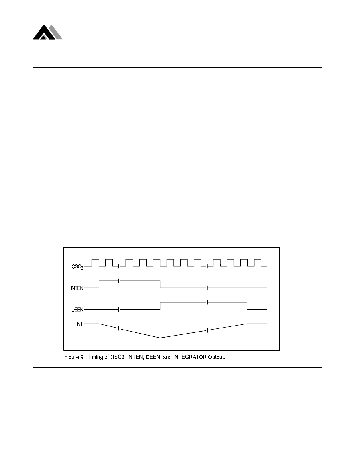
Integration Status (INTEN)
The INTEN is an output signal of the converter, it is
“high” during the signal integration phase. This signal
can be used as a status indicator or a control to connect the analog signal to the converter for processing.
It is available in 44 pin package.
De-integration Status (DEEN)
The DEEN is an output signal of the converter, it is
“high” during the reference de-integration phase. The
period of the DEEN is proportional to the conversion
result. Users may calculate the conversion result by
counting the number of clock pulse on the OSC3 pin
when DEEN is “high”. The conversion result is equal
to (N/4) - 1/2 where N is the number of the pulse at the
OSC3 pin. It is available in 44 pin package.
nn
n Component Value Selection
nn
Auto-Zero Capacitor (Caz)
The Caz capacitor size has some influence on system
noise. A 0.47µF capacitor is recommended for 200
mV full-scale applications. A 0.047µF capacitor is
recommended for 2.0V full-scale applications. A mylar
dielectric capacitor is adequate.
Reference Capacitor (Cref)
A 0.1µF capacitor is acceptable when “INLO” is tied
to analog common. If a large common-mode voltage
11

AME, Inc.
AME7106/AME7106A/AME7106R
AME7107/AME7107A/AME7107R
nn
n Component Value Selection
nn
Auto-Zero Capacitor (Caz)
The Caz capacitor size has some influence on system
noise. A 0.47µF capacitor is recommended for 200 mV
full-scale applications. A 0.047µF capacitor is recommended for 2.0V full-scale applications. A mylar dielectric capacitor is adequate.
Reference Capacitor (Cref)
A 0.1µF capacitor is acceptable when “INLO” is tied
to analog common. If a large common-mode voltage
exists and the application requires 200 mV full-scale,
increase Cref to 1.0 µF. A mylar dielectric capacitor is
adequate.
Integrating Capacitor (Cint)
Cint should be selected to maximize the integrator output voltage swing without causing output saturation. A
±2V full-scale integrator output swing is recommended
if “ANALOG COMMON” is used as signal reference.
For 3 readings/second (fosc = 48 KHz) a 0.22 µF value
is suggested. If a different oscillator frequency is used,
Cint must be changed in inverse proportion to maintain
the nominal 2V integrator swing. An exact expression
for Cint is:
Cint = [(4000)(1/fosc)(Vfs/Rint)] / Vint
where:
fosc= Oscillator clock frequency
Vfs = Full-scale input voltage
Rint = Integrating resistor
Vint = Desired full-scale integrator output swing
Cint must have low dielectric absorption to minimize
rollover error. A polypropylene capacitor is recommended.
Integrating Resistor (Rint)
The input buffer amplifier and integrator both have a
class A output stage with 100 µA quiescent current.
The integrator and buffer can supply 20 µA drive currents with negligible linearity errors. Rint is chosen to
keep the output stage in the linear region. For a 200mV
full-scale, it is 47KΩ; 2.0V full-scale requires 470KΩ.
3-1/2 Digit A/D Converter
High Accuracy, Low Power
Oscillator Components
R-C Oscillator
A 100 KΩ Rosc is recommended for all frequencies.
Cosc is selected by using the equation:
fosc = 0.45/(RC)
For fosc of 48KHz, Cosc is 100pF nominally.
To achieve maximum line noise rejection, the signal-
integrate period should be a multiple of line period. The
optimum oscillator frequencies for 60 Hz and 50 Hz
rejection are listed as follows:
For 60 Hz rejection:
40KHz, 48KHz, 60KHz etc.
For 50 Hz rejection:
40KHz, 50KHz, 66-2/3KHz etc.
Reference Voltage Selection
A full-scale reading (2000 counts) requires the input
signal be twice the reference voltage.
F u ll-S c a le Vo lta g e V re f
200.0 m V 100.0 m V
2.000 V 1.000 V
In some applications a scale factor other than unity may
exist between a transducer output voltage and the required digital reading. Assume, for example, a pressure transducer output is 600 mV for 2000 Ib/in2. Rather
than dividing the input voltage by three the reference
voltage should be set to 300 mV . This permits the transducer input to be used directly. The integrator resistor
would be 120KΩ. In some temperature and weighting
system with variable tare, the offset reading can be
generated by connecting the voltage transducer between INHI and COMMON and the variable offset voltage between COMMON and INLO.
Summary of component selection:
Full scale 200.0m V 2.000V
Caz 0.47µF0.047µF
R int 47 K
Cint 0.22µF0.22
Vref 100.0mV 1.000V
Note: fosc = 48 KHz
12
Ω
470 K
Ω
F
µ

AME, Inc.
AME7106/AME7106A/AME7106R
AME7107/AME7107A/AME7107R
Power Supplies
The AME7107 is designed to work from ±5V supplies.
However, if a negative supply is not available, it can be
generated from the clock output with two diodes, two
capacitors, and an inexpensive IC. The 7660 DC to DC
converter may also be used to generate -5V from +5V.
Low Battery Flag (LB)
The low battery flag is set when the supply voltage (V+
to V-) is lower than seven volts, typical. Once the LB is
set, the waveform of the LB will be out of phase with
the BP (Back Plane) to turn on a low battery annunciator for AME7106; LB pin will be low (Ground)
3-1/2 Digit A/D Converter
High Accuracy, Low Power
for AME7107 and is capable to sink 8 mA to turn on a
LED indicator.
AME7107 Power Dissipation Reduction
The AME7107 sinks the LED display current and this
generates heat in the IC package. If the internal voltage reference is used, the fluctuating chip temperature
can cause the display to change reading. The AME7107
package power dissipation can be reduced by reducing
the LED common anode voltage.
A typical LED has 1.8 volts across it, at 7mA. When its
common anode is connected to +5V, the AME7107
13

AME, Inc.
AME7106/AME7106A/AME7106R
AME7107/AME7107A/AME7107R
output is at 3.2V . Maximum power dissipation is 8.1 mA
X 3.2 V X 24 segments = 622mW. However, once the
AME7107 output voltage is above two volts, the LED current is essentially constant as output voltage increases.
Reducing the output voltage by 0.7V , results in 7.7mA of
LED current, only a 5 percent reduction. Maximum power
dissipation is only 7.7mA X 2.5V X 24 = 462 mW, a reduction of 26%. An output voltage reduction of 1 volt
reduces LED current by 10% (7.3mA) power dissipation
by 38%. (7.3mA X 2.2V X 24 = 385mW).
There are two ways to reduce the power dissipation:
either a 5.1 ohm resistor or a 1 Amp diode placed in
series with the display (but not in series with the
AME7107). The resistor will reduce the AME7107 output voltage, when all 24 segments are “ON”. When
segments turn off, the output voltage will increase. The
3-1/2 Digit A/D Converter
High Accuracy, Low Power
diode, on the other hand, will result in a relatively steady
output voltage.
In addition to limiting maximum power dissipation, the
resistor reduces the change in power dissipation as the
display changes. As fewer segments are “ON,” each
“ON” output drops more voltage and current. For the
best case of six segments (a “111” display) to worst
case (a “1888” display) the resistor will change about
230 mW. While a circuit without the resistor will change
about 470 mW. Therefore, the resistor will reduce the
variation of power dissipation by about 50%.
The change in LED brightness caused by the resistor is
almost unnoticeable as more segments turn off. If steady
display brightness is very important, a diode is recommended.
nn
n T ypical Applications
nn
14

AME, Inc.
AME7106/AME7106A/AME7106R
AME7107/AME7107A/AME7107R
3-1/2 Digit A/D Converter
High Accuracy, Low Power
15

AME, Inc.
AME7106/AME7106A/AME7106R
AME7107/AME7107A/AME7107R
3-1/2 Digit A/D Converter
High Accuracy, Low Power
16

AME, Inc.
AME7106/AME7106A/AME7106R
AME7107/AME7107A/AME7107R
3-1/2 Digit A/D Converter
High Accuracy, Low Power
17

AME, Inc.
AME7106/AME7106A/AME7106R
AME7107/AME7107A/AME7107R
3-1/2 Digit A/D Converter
High Accuracy, Low Power
18

AME, Inc.
AME7106/AME7106A/AME7106R
AME7107/AME7107A/AME7107R
nn
n Package Dimension
nn
PDIP-40
SYMBOLS
A
A
B
B
D
E
F
e
E
θθθθ
3-1/2 Digit A/D Converter
High Accuracy, Low Power
MILLIMETERS INCHES
MIN MAX MIN MAX
0.150 0.165 0.0059 0.0065
1
1
1
B
0.072 (TYP) 0.0028
0.018(TYP) 0.0007
0.050(TY P) 0.0020
2.049 2.074 0.0807 0.0817
0.540 0.555 0.0213 0.0219
0.600(TY P) 0.0236
0.100(TY P) 0.0039
0.600 0.700 0.0236 0.0276
o
0
15
o
o
0
15
o
19

www.ame.com.tw
E-Mail: info@ame.com.tw
Life Support Policy:
These products of AME, Inc. are not authorized for use as critical components in life-support devices or
systems, without the express written approval of the president
of AME, Inc.
AME, Inc. reserves the right to make changes in the circuitry and specifications of its devices and
advises its customers to obtain the latest version of relevant information.
ã AME, Inc. , February 2002
Document: 1021-DS7106/7107-C
U.S. Headquarter Corporate Headquarter
Analog Microelectronics, Inc. AME, Inc.
3100 De La Cruz Blvd. Suite 201 2F , 189 Kang-Chien Road, Nei-Hu District
Santa Clara, CA. 95054-2046 Taipei 114, Taiwan, R.O.C.
Tel : (408) 988-2388 Tel : 886 2 2627-8687
Fax: (408) 988-2489 Fax: 886 2 2659-2989
 Loading...