

Analog Microelectronics AME1084DCDT-3, AME1084DCDT, AME1084DCCS, AME1084DCBT, AME1084CCDT-3 Datasheet
...
Analog Microelectronics, Inc.
AME1084
nn
n General Description
nn
The AME1084 is a 5A low-dropout positive voltage regulator. It is available in fixed and adjustable output voltage versions. Overcurrent and thermal protection are
integrated onto the chip. Output current will limit as it
reaches the pre-set current or temperature limit. At full
rated output current the dropout voltage is 1.4V (max.).
AME1084 series regulators provide excellent regulation
over line, load and temperature variations.
nn
n Applications
nn
ll
l High Efficiency Linear Regulators
ll
ll
l Post Regulators for Switching Supplies
ll
ll
l 5V to 3.3V Voltage Converter
ll
ll
l Battery Charger
ll
5A Low Dropout
Positive Voltage Regulator
nn
n Key Features
nn
l Low dropout voltage
ll
l Adjustable or 3.3V fixed voltage
ll
ll
l Line regulation typically 0.015%
ll
ll
l Load regulation typically 0.05%
ll
ll
l Adjust pin (ADJ) current less than 90µA
ll
ll
l Overcurrent protection
ll
ll
l Thermal protection
ll
ll
l Available in TO-220, TO-263, TO-252
ll
…
1.4V at 5A
nn
n Functional Block Diagram
nn
Current
Limiting
Amplifier
Thermal
Protection
Error
Amp.
Bandgap
Reference
Figure 1
Input
Output
ADJ/GND
nn
n Typical Application
nn
4.75V to 5.25V
10
V
IN
µ
F Tan
AME1084
GND
Figure 2
V
OUT
10
µ
F Tan
Load
1

Analog Microelectronics, Inc.
AME1084
nn
n Pin Configuration
nn
AME1084
ADJ/GND
TO-220 Front View
V
OUT
5A Low Dropout
Positive Voltage Regulator
AME 1084
1
ADJ/GND
V
IN
V
To-252 Front View
2
OUT
3
V
IN
AME 1084
1
ADJ/GND
TO-263-2 Front View
V
2
OUT
3
V
IN
AME 1084
1
ADJ/GND
TO-263-3 Front View
V
2
OUT
3
V
IN
2

Analog Microelectronics, Inc.
AME1084
nn
n Ordering Information
nn
Part Numbe r Markin g Outp ut Vo lta g e Packa g e
AM E 1084
AM E 1084A CB T
AME1084BCBT
AM E1084CCBT
AM E1084DCBT
AM E1084ACDT-3
AM E1084BCDT-3
AM E 1084CCDT-3
AM E 1084DCDT-3
AM E 1084A CDT
AM E1084BCDT
AM E 1084CCDT
AM E 1084DCDT
AM E 1084A CCS
AM E1084BCCS
AM E 1084CCCS
AM E 1084DCCS
ACBT
yyww
AM E 1084
BCB T
yyww
AM E 1084
CCBT
yyww
AM E 1084
DCBT
yyww
AM E 1084
ACDT-3
yyww
AM E 1084
BCDT-3
yyww
AM E 1084
CCDT-3
yyww
AM E 1084
DCDT-3
yyww
AM E 1084
ACDT
yyww
AM E 1084
BCDT
yyww
AM E 1084
CCDT
yyww
AM E 1084
DCDT
yyww
AM E 1084
ACCS
yyww
AM E 1084
BCCS
yyww
AM E 1084
CCCS
yyww
AM E 1084
DCCS
yyww
5A Low Dropout
Positive Voltage Regulator
ADJ TO-220
1.5 TO-220
2.5 TO-220
3.3 TO-220
ADJ TO-263-3
1.5 TO-263-3
2.5 TO-263-3
3.3 TO-263-3
ADJ TO-263-2
1.5 TO-263-2
2.5 TO-263-2
3.3 TO-263-2
ADJ TO-252
1.5 TO-252
2.5 TO-252
3.3 TO-252
3

Analog Microelectronics, Inc.
AME1084
nn
n Absolute Maximum Ratings
nn
Param eter
Inpu t V o l tag e
TO-220 3
Thermal Resistance (Junction to Case)
Thermal Res i s tance (Junct i on t o A m bi ent )
Operating Junc t i on Temperature Range T
St orage Temperature Range T
Lead Temperature (10 sec) T
TO-252 5
TO-263 3
TO-220 50
TO-252 90
TO-263 50
Positive Voltage Regulator
Symbol Maximum Unit
V
IN
θ
JC
θ
JA
J
STG
LEAD
7V
o
C/W
0 to 125
-65 to 150
260
o
C
5A Low Dropout
4
Analog Microelectronics, Inc.
O
0
AME1084
nn
n Electrical Characteristics
nn
1. 1084AXXX
Parameter Symbol Min. Typ. Max. Units
Reference voltage V
(adjustable volt age) I
Line regulat ion
Load regulation
Dropout volt age V
∆V
OUT
, ∆V
= 1% IO = 10m A - 5A Over temp. - 1.3 -
REF
Current limit I
Temperat ure Coefficient T
Adjust pi n c urrent
Adjust pi n c urrent c hange 0.2 5 Temperat ure s tability T
Mini m um l oad c urrent I
RMS out put noi se V
Ripple rejection ratio
V
Reg
Reg
∆
V
I
ADJ
R
REF
LIN E
LOAD
D
S
C
I
ADJ
S
O
N
A
= 5V TJ =25OC 1.238 1.262
IN
= 10mA Over temp. 1.225 1.275
O
= 2. 75 - 7V TJ =25OC-0.0150.2
V
IN
= 10mA Over temp. - 0.035 0.2
I
O
= 5V TJ =25OC - 0.05 0.3
V
IN
= 10mA - 5A Over temp. - 0.2 0.4
I
O
= 2. 75 - 7V TJ =25OC-1.21.4
IN
VIN = 2.75 - 7V, Over temp. 5.0 - - A
VIN = 2. 75 - 7V, IO = 10 m A - 5A - 0. 00 5 -
= 2. 75 - 7V TJ = 25OC- 55 -
V
IN
= 10m A - 5A Over temp. - - 90
I
O
V
= 2. 75 - 7V, IO = 10 m A - 5A
IN
Over temp.
V
= 5V, IO = 500m A , Over temp. 0.5 0.5 - %
IN
VIN = 5V - 5 10 mA
TJ = 25OC-0.003-%V
VIN = 5V, IO = 5A, Over temp.
Test Conditions
5A Low Dropout
Positive Voltage Regulator
1.250
60 72 - dB
%/
V
%
%
V
C
A
µ
O
2. 1084DXXX
Pa rameter Symbol Min. Typ. Max. Units
Output volt age V
Vo 3.300
(fixed voltage) I
Line regulati on Reg
Load regulation Reg
Dropout voltage V
∆V
OUT
, ∆V
= 1% IO = 0A - 5A Over temp. - 1.3 -
REF
Current limit I
Quiescent current
(fixed model)
Temperature Coefficient T
Temperature st abilit y T
RMS output noise V
Ripple rejection ratio
LOAD
V
S
I
Q
R
LIN E
D
C
S
N
A
Test Conditions
= 5V TJ =25OC 3.267 3.333
IN
= 0A Over temp. 3.234 3.366
O
= 4. 5 - 7V TJ =25OC-0.0150.2
V
IN
I
= 0A Over temp. - 0.035 0.2
O
= 5V TJ =25OC - 0.05 0.3
V
IN
= 0A - 5A Over temp. - 0.2 0.4
I
O
= 4. 5 - 7V TJ =25OC-1.21.4
IN
VIN = 4. 5 - 7V, Over t emp. 5. 0 - - A
VIN=5V, Io=0-5A, Over temp. - 13 mA12
VIN = 4. 5 - 7V, IO = 0A - 5A - 0. 005 V
= 5V , IO = 500m A , Over tem p. 0.5 0.5 - %
IN
T
= 25OC
J
VIN = 5V, IO = 5A, Over temp.
- 0.003 - %V
60 72 - dB
%/
V
%
%
V
C
O
5

Analog Microelectronics, Inc.
AME1084
nn
n Application Description
nn
1. Output voltage adjustment
Like most regulators, the AME1084 regulates
the output by comparing the output voltage to
an internally generated reference voltage. On
the adjustable version, the VREF is available externally as 1.25V between V
voltage ratio formed by R1 and R2 should be
set to conduct 10mA (minimum output load).
The output voltage is given by the following
equation:
V
= V
OUT
REF
R2
( 1 + ) + I
R1
On fixed versions of AME1084, the voltage divider is provided internally.
V
IN
IN
ADJ
C
1
I
ADJ
50µA
R2
V
OUT
= V
REF
(1+
) + I
R1
and ADJ. The
OUT
ADJ
OUT
x R2
ADJ
x R2
V
REF
R1
R2
Positive Voltage Regulator
3. Current limit protection
AME1084 is protected against overload conditions.
Current protection is triggered at typical 7.5A.
4. Stability and load regulation
AME1084 requires a capacitor from VOUT to GND t o
provide compensation feedback to the internal gain
stage. This is to ensure stability at the output terminal. Typically, a 10µF tantalum or 5 0 µF aluminum
electrolytic is sufficient.
Note: It is important that the ESR for this capacitor
does not exceed 0.5Ω.
The output capacitor dose not have a theoretical
upper limit and increasing its value will increase
stability . COUT = 100µF or more is typical for high current regulator design.
For the adjustable version, the best load regulation is
V
OUT
accomplished when the top of theresistor divider
(R1) is connected directly to theoutput pin of the
AME1084. When so connected, RP is not multiplied
by the divider ratio.
For fixed output versions, the top of R1 is internally
connected to the output. The ground pin can be connected to low side of the load to eliminate ground loop
errors.
5A Low Dropout
2. Thermal protection
AME1084 has thermal protection which limits
junction temperature to 150OC. However, device functionality is only guaranteed to a maximum junction temperature of +125OC.
The power dissipation and junction temperature for AME1084 in TO-220 package are given
by
PD = (VIN - V
T
Note: T
6
JUNCTION
JUNCTION
= T
Figure 3
) x I
OUT
OUT
+ ( PD x θJA)
AMBIENT
must not exceed 125OC
R
P
Parasitic
Line Resistance
V
IN
IN
OUT
ADJ
R1
(Connect R1 to case)
R
L
R2
Connect
R2 to load
Figure 4

Analog Microelectronics, Inc.
AME1084
5. Thermal consideration
The AME1084 series contain thermal limiting
circuitry designed to protect itself for overtemperature conditions. Even for normal load
conditions, maximum junction temperature
ratings must not be exceed. As mention in
thermal protection section, we need to consider all sources of thermal resistance between junction and ambient. It includes junction-to-case, case-to-heat-sink interface and
heat sink thermal resistance itself.
Junction-to-case thermal resistance is specified from the IC junction to the bottom of the
case directly below the die. Proper mounting
is required to ensure the best possible thermal flow from this area of the package to the
heat sink. The case of all devices in this series is electrically connected to the output.
Therefore, if the case of the device must be
electrically isolated, a thermally conductive
spacer is recommended.
5A Low Dropout
Positive Voltage Regulator
7

Analog Microelectronics, Inc.
AME1084
nn
n Advanced Applications
nn
V
= 5V
IN
10µF
µ
10
* VO = V
** Optional for improved ripple rejection
5A Low Dropout
Positive Voltage Regulator
AME1084
V
IN
V
OUT
* VO = 1.5 - 3.45V
ADJ
R1
2K
R2
R1
1K
ADJ
x R2
F
**
REF
R2
(1 + ) + I
10µF
Figure 5 Adjustable Output V oltage
V
IN
10µF
* 20mW is ballast resistance
The inter - connection of #18 wire could act as ballast resistance
AME1084
V
IN
GND
AME1084
V
IN
GND
V
V
OUT
OUT
R1
* 20m
R2
* 20m
Ω
Ω
V
O
= 0 to 10A
I
O
10µF
Figure 6 Paralleling Regulators
8

Analog Microelectronics, Inc.
AME1084
nn
n Advanced Applications (Cont.)
nn
V
IN
10µF
µ
F
10
* VO = V
** Optional for improved ripple rejection
+ VZ (VZ: breakdown voltage of Zener diode)
REF
AME1084
V
IN
**
GND
V
OUT
1K
Zener diode or
voltage reference
5A Low Dropout
Positive Voltage Regulator
*
V
O
10µF
Figure 7 Regulator with Reference
*
AME1084
V
IN
V
OUT
GND
10µF
Figure 8 Regulator with Reverse Diode Protection
100
V
O
µ
F
9

Analog Microelectronics, Inc.
AME1084
nn
n Performance Characteristics
nn
Drop-out Voltage vs. Load Current
1.30
1.25
1.20
1.15
1.10
1.05
1.00
Drop-out Volatge (V)
0.95
0.90
012345
5A Low Dropout
Positive Voltage Regulator
Minimum Operation Current vs
Input/Output Differential V oltage
7
6
5
4
3
2
1
0
Minimum Operation Current (mA)
0123456789
Load Current (A)
9
8
7
6
5
4
3
2
1
Output Short Circuit Current (A)
0
Input/Output Differential Voltage(V)
Output Short circuit Current vs
Input/Output Differential V oltage
123456789
Input/Ou tput Differen tial Voltage(V)
10

Analog Microelectronics, Inc.
AME1084
nn
n External Resistor Divider Table for Customized Voltage
nn
R1(ohm) 100 102 105 107 110 113 115 118 121 124
Vout
1.25 0.000 0.000 0.000 0.000 0.000 0.000 0.000 0.000 0.000 0.000
1.30 3.984 4.063 4.182 4.262 4.381 4.500 4.579 4.698 4.817 4.936
1.35 7.968 8.127 8.365 8.524 8.761 8.999 9.158 9.396 9.633 9.871
1.40 11.95 12.19 12.55 12.79 13.14 13.50 13.74 14.09 14.45 14.81
1.45 15.94 16.25 16.73 17.05 17.52 18.00 18.32 18.79 19.27 19.74
1.50 19.92 20.32 20.91 21.31 21.90 22.50 22.89 23.49 24.08 24.68
1.55 23.90 24.38 25.09 25.57 26.28 27.00 27.47 28.19 28.90 29.61
1.60 27.89 28.44 29.28 29.83 30.67 31.50 32.05 32.88 33.72 34.55
1.65 31.87 32.51 33.46 34.09 35.05 36.00 36.63 37.58 38.53 39.48
1.70 35.86 36.57 37.64 38.36 39.43 40.50 41.21 42.28 43.35 44.42
1.75 39.84 40.63 41.82 42.62 43.81 45.00 45.79 46.98 48.17 49.36
1.80 43.82 44.70 46.01 46.88 48.19 49.50 50.37 51.68 52.98 54.29
1.85 47.81 48.76 50.19 51.14 52.57 54.00 54.95 56.37 57.80 59.23
1.90 51.79 52.82 54.37 55.40 56.95 58.50 59.53 61.07 62.62 64.16
1.95 55.78 56.89 58.55 59.66 61.33 63.00 64.11 65.77 67.43 69.10
2.00 59.76 60.95 62.74 63.93 65.71 67.49 68.68 70.47 72.25 74.03
2.05 63.75 65.01 66.92 68.19 70.09 71.99 73.26 75.17 77.07 78.97
2.10 67.73 69.08 71.10 72.45 74.47 76.49 77.84 79.86 81.88 83.90
2.15 71.71 73.14 75.28 76.71 78.85 80.99 82.42 84.56 86.70 88.84
2.20 75.70 77.21 79.47 80.97 83.23 85.49 87.00 89.26 91.52 93.77
2.25 79.68 81.27 83.65 85.24 87.61 89.99 91.58 93.96 96.33 98.71
2.30 83.67 85.33 87.83 89.50 92.00 94.49 96.16 98.65 101.2 103.6
2.35 87.65 89.40 92.01 93.76 96.38 98.99 100 .7 103.4 106 .0 108.6
2.40 91.63 93.46 96.20 98.02 100.8 103.5 105 .3 108.1 110.8 113.5
2.45 95.62 97.52 100.4 102.3 105.1 108.0 109 .9 112.7 115.6 118.5
2.50 99.60 101.6 104.6 106.5 109.5 112.5 114 .5 117.4 120.4 123.4
2.55 103.6 105.6 108.7 110.8 113.9 117.0 119 .1 122 .1 125.2 128.3
2.60 107.6 109.7 112.9 115.1 118.3 121.5 123 .6 126 .8 130.1 133.3
2.65 111.6 113.8 117.1 119.3 122.7 126.0 128 .2 131 .5 134.9 138.2
2.70 115.5 117.8 121.3 123.6 127.0 130.5 132 .8 136 .2 139.7 143.1
2.75 119.5 121.9 125.5 127.9 131.4 135.0 137 .4 140 .9 144.5 148.1
2.80 123.5 126.0 129.7 132.1 135.8 139.5 141 .9 145 .6 149.3 153.0
2.85 127.5 130.0 133.8 136.4 140.2 144.0 146 .5 150 .3 154.1 157.9
2.90 131.5 134.1 138.0 140.6 144.6 148.5 151 .1 155 .0 159.0 162.9
2.95 135.5 138.2 142.2 144.9 148.9 153.0 155 .7 159 .7 163.8 167.8
3.00 139.4 142.2 146.4 149.2 153.3 157.5 160 .3 164 .4 168.6 172.7
3.05 143.4 146.3 150.6 153.4 157.7 162.0 164 .8 169 .1 173.4 177.7
3.10 147.4 150.3 154.8 157.7 162.1 166.5 169 .4 173 .8 178.2 182.6
R2(ohm)=(Vou t-1.25)*R1/(1.25+50u*R1)
Positive Voltage Regulator
5A Low Dropout
11

Analog Microelectronics, Inc.
AME1084
nn
n External Resistor Divider Table for Customized Voltage
nn
R1(ohm) 100 102 105 107 110 113 115 118 121 124
Vout
3.15 151.4 154.4 158.9 161.9 166.5 171.0 174 .0 178 .5 183.0 187.5
3.20 155.4 158.5 163.1 166.2 170.8 175.5 178 .6 183 .2 187.9 192.5
3.25 159.4 162.5 167.3 170.5 175.2 180.0 183 .2 187 .9 192.7 197.4
3.30 163.3 166.6 171.5 174.7 179.6 184.5 187 .7 192 .6 197.5 202.4
3.35 167.3 170.7 175.7 179.0 184.0 189.0 192 .3 197 .3 202.3 207.3
3.40 171.3 174.7 179.8 183.3 188.4 193.5 196 .9 202 .0 207.1 212.2
3.45 175.3 178.8 184.0 187.5 192.8 198.0 201 .5 206 .7 211.9 217.2
3.50 179.3 182.9 188.2 191.8 197.1 202.5 206 .1 211 .4 216.8 222.1
3.55 183.3 186.9 192.4 196.0 201.5 207.0 210 .6 216 .1 221.6 227.0
3.60 187.3 191.0 196.6 200.3 205.9 211.5 215 .2 220 .8 226.4 232.0
3.65 191.2 195.0 200.8 204.6 210.3 216.0 219 .8 225 .5 231.2 236.9
3.70 195.2 199.1 204.9 208.8 214.7 220.5 224 .4 230 .2 236.0 241.8
3.75 199.2 203.2 209.1 213.1 219.0 225.0 228 .9 234 .9 240.8 246.8
3.80 203.2 207.2 213.3 217.3 223.4 229.5 233 .5 239 .6 245.7 251.7
3.85 207.2 211.3 217.5 221.6 227.8 234.0 238 .1 244 .3 250.5 256.6
3.90 211.2 215.4 221.7 225.9 232.2 238.5 242 .7 249 .0 255.3 261.6
3.95 215.1 219.4 225.9 230.1 236.6 243.0 247 .3 253 .7 260.1 266.5
4.00 219.1 223.5 230.0 234.4 240.9 247.5 251 .8 258 .4 264.9 271.5
4.05 223.1 227.6 234.2 238.7 245.3 252.0 256 .4 263 .1 269.7 276.4
4.10 227.1 231.6 238.4 242.9 249.7 256.5 261 .0 267 .8 274.6 281.3
4.15 231.1 235.7 242.6 247.2 254.1 261.0 265 .6 272 .5 279.4 286.3
4.20 235.1 239.7 246.8 251.4 258.5 265.5 270 .2 277 .2 284.2 291.2
4.25 239.0 243.8 250.9 255.7 262.8 270.0 274 .7 281 .9 289.0 296.1
4.30 243.0 247.9 255.1 260.0 267.2 274.5 279 .3 286 .6 293.8 301.1
4.35 247.0 251.9 259.3 264.2 271.6 279.0 283 .9 291 .3 298.6 306.0
4.40 251.0 256.0 263.5 268.5 276.0 283.5 288 .5 296 .0 303.5 310.9
4.45 255.0 260.1 267.7 272.8 280.4 288.0 293 .1 300 .7 308.3 315.9
4.50 259.0 264.1 271.9 277.0 284.7 292.5 297 .6 305 .4 313.1 320.8
4.55 262.9 268.2 276.0 281.3 289.1 297.0 302 .2 310 .1 317.9 325.7
4.60 266.9 272.2 280.2 285.5 293.5 301.5 306 .8 314 .8 322.7 330.7
4.65 270.9 276.3 284.4 289.8 297.9 306.0 311 .4 319 .5 327.5 335.6
4.70 274.9 280.4 288.6 294.1 302.3 310.5 315 .9 324 .2 332.4 340.6
4.75 278.9 284.4 292.8 298.3 306.7 315.0 320 .5 328 .8 337.2 345.5
4.80 282.9 288.5 297.0 302.6 311.0 319.5 325 .1 333 .5 342.0 350.4
4.85 286.9 292.6 301.1 306.8 315.4 324.0 329 .7 338 .2 346.8 355.4
4.90 290.8 296.6 305.3 311.1 319.8 328.5 334 .3 342 .9 351.6 360.3
4.95 294.8 300.7 309.5 315.4 324.2 333.0 338 .8 347 .6 356.4 365.2
5.00 298.8 304.8 313.7 319.6 328.6 337.5 343 .4 352 .3 361.3 370.2
R2(ohm)=(Vou t-1.25)*R1/(1.25+50u*R1)
Positive Voltage Regulator
5A Low Dropout
12
Analog Microelectronics, Inc.
*
AME1084
nn
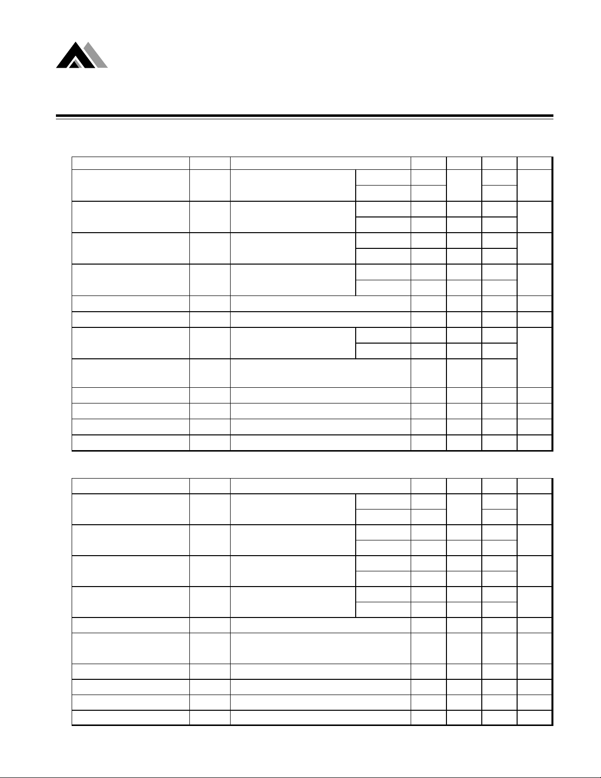
n Package Dimension
nn
TO-220
5A Low Dropout
Positive Voltage Regulator
SYMBOLS
A 4.06 4.83 0.160 0.190
b 0.63 1.02 0.025 0.040
C1 0.35 0.60 0.0138 0.0236
D 14.22 14.99 0.056 0.590
E 9.66 10.54 0.385 0.415
e - 2.79 - 0.110
e1 4.83 5.33 0.190 0.210
e3 1.14 1.40 0.045 0.055
f 1.14 1.40 0.045 0.055
H1 5.94 6.55 0.234 0.258
K 2.29 2.92 0.090 0.115
CP 3.71 3.96 0.146 0.156
Q 2.62 2.87 0.103 0.113
L 12.70 14.27 0.500 0.5618
a 3D7D3D7D
b1 1.14 1.52 0.0449 0.06
R
Notes :
1. Dim ension C1 apply for tin plate finish.
2. For solder dip lead finish dim ension C1 should be
0.015"-0.027" (0.38-0.69)
MILLIMETERS INCHES
MIN MAX MIN MA X
6.17 REF. 0.243 REF.
TO-263-3
SYM B OLS
A 9.65 10.41 0.380 0.410
B 8.28 9.65 0.326 0.380
C 4.06 4.83 0.160 0.190
D 0.51 1.02 0.020 0.040
E 1.14 1.40 0.045 0.055
G
H 14.61 15.88 0.575 0.625
K 1.02 1.68 0.040 0.066
L 0.00 0.97 0.000 0.038
M 2.49 2.74 0.098 0.108
N 0.43 0.58 0.017 0.023
P 2.29 2.79 0.090 0.110
R
S 2.41 2.67 0.095 0.105
W 0.254 0.508 0.010 0.020
: Ty pic al value
NO TES :
1. CONTRO LLING D IM ENSION : M ILLIMETER S .
2MAXIMUM LEAD TH IC K NESS INCLUDES LEAD FINISH
THICKNESS
MINIMUM LEAD THICKNESS IS THE MINIMUM
THICKNESS OF BASE MATER IA.
MILLIM ETERS INCHES
MIN MAX MIN MAX
*
2.54
o
0
?
8
*
0.100
o
0
8
?
13

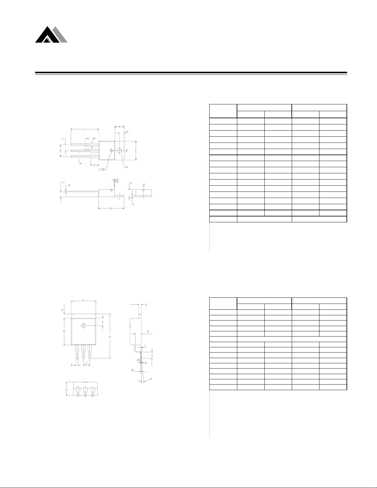
Analog Microelectronics, Inc.
*
AME1084
nn
n Package Dimension
nn
TO-263-2
5A Low Dropout
Positive Voltage Regulator
SY MBO L S
A 9.65 10.41 0.380 0.410
B 8.28 9.65 0.326 0.380
C 4.06 4.83 0.160 0.190
D 0.51 1.02 0.020 0.040
E 1.14 1.40 0.045 0.055
G
H 14.61 15.88 0.575 0.625
K 1.02 1.68 0.040 0.066
L 0.00 0.97 0.000 0.038
M 2.49 2.74 0.098 0.108
N 0.43 0.58 0.017 0.023
P 2.29 2.79 0.090 0.110
R
S 2.41 2.67 0.095 0.105
W 0.254 0.508 0.010 0.020
: Typical value
MILLIMETERS INCHES
MIN MAX MIN MAX
*
2.54
o
0
?
8
*
0.100
o
0
?
8
NOTES :
1. CONTROLLING DIMENSION : MILLIMETERS.
2MAXIMUM LEAD THICKNESS INCLUDES LEAD FINISH
THICKNESS
MINIMUM LEA D TH ICKNES S I S THE MINIMUM
THICKNESS OF BASE MATERIA.
14

Analog Microelectronics, Inc.
AME1084
nn
n Package Dimension
nn
TO-252 (DPAK)
5A Low Dropout
Positive Voltage Regulator
SYMB OLS
A 0.45 0.58 0.0177 0.023
B 1.60 1.95 0.06 0.0768
C 0.51 - 0.02 D 0.45 0.60 0.0177 0.0236
E 6.40 6.80 0.252 0.2677
F 5.40 5.80 0.2126 0.2283
G 2.20 2.85 0.0866 0.1122
H - * 2.30 - * 0.0906
I - 0.90 - 0.0354
J - 0.97 - 0.038
K 5.20 5.50 0.20 0.22
L 0.89 2.03 0.035 0.08
* : Typical value
NOTES :
1. CONTROLLING DIM E NS ION : MILLIMETERS .
2. MAXIMUM LEAD THICKNESS INCLUDES LEAD FINISH THICKNESS
MINIMUM LEAD THICKNESS IS THE MINIMUM THICKNESS OF BASE
MATERIAL.
MILLIMETERS INCHES
MIN MAX MIN MAX
TO-252 (DPAK)
SYMBOLS
A 0.45 0.58 0.0177 0.023
B 1.60 1.95 0.06 0.0768
C0.51 - 0.02 D 0.45 0.60 0.0177 0.0236
E 6.40 6.80 0.252 0.2677
F 5.40 5.80 0.2126 0.2283
G 2.20 2.85 0.0866 0.1122
H - * 2.30 - * 0.0906
I - 0.90 - 0.0354
J - 0.97 - 0.038
K 5.20 5.50 0.20 0.22
L 0.89 2.03 0.035 0.08
* : Typical value
NOTES :
1. CONTROLLING DIMENSION : M ILLIM ETERS.
2. MAXIMUM LEAD THICKNESS INCLUDES LEAD FINISH THICKNESS
MINIMUM LEAD THICKNESS IS THE MINIMUM THICKNESS OF BASE
MATERIAL.
MILLIMETERS INCHES
MIN MAX MIN MAX
15

www.analogmicro.com
E-Mail: info@analogmicro.com
Life Support Policy:
These products of Analog Microelectronics, Inc. are not authorized for use as critical components in life-
support devices or systems, without the express written approval of the president
of Analog Microelectronics, Inc.
Analog Microelectronics, Inc. reserves the right to make changes in the circuitry and specifications of its
devices and advises its customers to obtain the latest version of relevant information.
Analog Microelectronics, Inc. , July 2001
Document: 1012-doc-B-0704
Corporate Headquarters Asia Pacific Headquarters
Analog Microelectronics, Inc. AME, Inc.
3100 De La Cruz Blvd. Suite 201 2F, 187 ,Kang-Chien Rd, Nei-Hu District
Santa Clara, CA. 95054-2046 Taipei 114, Taiwan, R.O.C.
Tel : (408) 988-2388 Tel : 886 2 2627-8687
Fax: (408) 988-2489 Fax : 886 2 2659-2989
 Loading...