

Analogic Technologies AAT3236IJS-3.5-T1, AAT3236IJS-3.3-T1, AAT3236IJS-3.0-T1, AAT3236IJS-2.85-T1, AAT3236IJS-2.8-T1 Datasheet
...
AAT3236
300mA CMOS High Performance LDO
General Description
The AAT3236 is a MicroPower™ Low Dropout
Linear Regulator designed to deliver a continuous
300mA output load current and is capable of handling short duration current peaks up to 500mA.
With a very small footprint SOT23-5 package it is
ideally suited for portable applications where low
noise, high power supply ripple rejection, extended
battery life and small size are critical. The AAT3236
features fast transient response and low output self
noise for powering sensitive RF circuitry. Other features include low quiescent current, typically
100µA, and low dropout voltage, typically 300mV at
full output load current. The device has internal output short circuit protection and thermal shutdown to
prevent damage under extreme conditions.
The AAT3236 also features a low-power shutdown
mode for longer battery life. A bypass pin is provided to improve PSRR performance by connecting an external capacitor from the AAT3236's reference output to ground.
PowerLinear
Features
• 500mA Peak Output Current
• Low Dropout - Typically 300mV at 300mA
• Guaranteed 300mA Output
• High accuracy ±1.5%
• 100µA Quiescent Current
• High Power Supply Ripple Rejection
• 70 dB at 1kHz
• 50 dB at 10kHz
• Very low self noise 45µVrms/rtHz
• Noise reduction bypass capacitor
• Short circuit protection
• Over-Temperature protection
• Shutdown mode for longer battery life
• Low temperature coefficient
• 7 Factory programmed output voltages
• SOT-23 5-pin or SC70JW 8-pin package
Applications
™
Preliminary Information
The AAT3236 is available in a space saving
SOT23-5 or SC70JW-8 package in 7 factory programmed voltages of 2.5V, 2.7V, 2.8V, 2.85V, 3.0V,
3.3V, or 3.5V.
• Cellular Phones
• Notebook Computers
• Portable Communication Devices
• Personal Portable Electronics
Typical Application
V
IN
IN
ON/OFF
1µF
GND GND
EN BYP
AAT3236
GND
OUT
10nF
2.2µF
V
OUT
3236.2001.11.0.9 1

Pin Descriptions
AAT3236
300mA CMOS High Performance LDO
Pin #
SOT23-5 SC70JW-8
1 5, 6 IN Input voltage pin - should be decoupled with 1µF or greater
2 8 GND Ground connection pin
3 7 EN Enable pin - this pin is internally pulled high. When pulled low
4 1 BYP Bypass capacitor connection - to improve AC ripple rejection,
5 2, 3, 4 OUT Output pin - should be decoupled with 2.2µF capacitor.
Symbol Function
capacitor.
the PMOS pass transistor turns off and all internal circuitry
enters low-power mode, consuming less than 1µA.
connect a 10nF capacitor to GND. This will also provide a soft
start function.
Pin Configuration
SOT-23-5 SC70JW-8
(Top View) (Top View)
IN
GND
EN
1 2
1
2
3
OUT
5
BYP
OUT
4
BYP
OUT
OUT
1
2
3
4
8
7
6
5
GND
EN
IN
IN
2 3236.2001.11.0.9

AAT3236
300mA CMOS High Performance LDO
Absolute Maximum Ratings (T
=25°C unless otherwise noted)
A
Symbol Description Value Units
V
IN
I
OUT
T
J
T
LEAD
Note: Stresses above those listed in Absolute Maximum Ratings may cause permanent damage to the device. Functional operation at conditions other than the operating conditions specified is not implied. Only one Absolute Maximum rating should be applied at any one time.
Input Voltage 6 V
DC Output Current PD/(VIN-VO)mA
Operating Junction Temperature Range -40 to 150 °C
Maximum Soldering Temperature (at leads, 10 sec) 300 °C
Thermal Information
Symbol Description Rating Units
Θ
JA
P
D
Note 1: Mounted on a demo board.
Maximum Thermal Resistance1(SOT23-5, SC70JW-8) 190 °C/W
Maximum Power Dissipation1(SOT23-5, SC70JW-8) 526 mW
Recommended Operating Conditions
Symbol Description Rating Units
V
IN
T Ambient Temperature Range -40 to +85 °C
Electrical Characteristics (V
TA= -40 to 85°C unless otherwise noted. For typical values TA=25°C)
Input Voltage (V
IN=VOUT(NOM)
+1V, I
=1mA, C
OUT
OUT
+0.3) to 5.5 V
OUT
= 2.2µF, CIN= 1µF, C
BYP
= 10nF,
Symbol Description Conditions Min Typ Max Units
T
=25°C -1.5 1.5 %
A
TA=-40 to 85°C -2.5 2.5 %
IN
100 150 µA
1 kHz 70
1MHz 47
∆V
∆V
V
OUT
I
OUT
V
DO
I
SC
I
Q
I
SD
∆V
OUT
V
OUT
OUT
OUT
V
EN(L)
V
EN(H)
I
EN
Output Voltage Tolerance I
Output Current V
Dropout Voltage
2
Short Circuit Current V
Ground Current VIN= 5V, no load,EN = V
Shutdown Current VIN= 5V, EN = 0V 1 µA
/ Line Regulation VIN= V
*∆V
IN
(line) Dynamic Line Regulation VIN=V
(load) Dynamic Load Regulation I
Enable Threshold Low 0.6 V
Enable Threshold High 1.5 V
Leakage Current Enable Pin VEN=5V 1 µA
PSRR Power Supply Rejection Ratio I
T
SD
T
HYS
e
T
Note 2: VDOis defined as VIN- V
Over Temp Shutdown Threshold 150 °C
Over Temp Shutdown Hysteresis 10 °C
Output Noise Noise Power BW= 300Hz to 50KHz 45 µV
N
Output Voltage Temp. Coeff. 22 ppm/°C
C
when V
OUT
OUT
OUT
I
OUT
OUT
I
=150mA, TR/TF=2µs
OUT
OUT
OUT
is 98% of nominal.
OUT
= 1mA to 300mA
> 1.2V 300 mA
= 300mA 300 500 mV
< 0.4V 600 mA
+ 1 to 5.5V 0.07 %/V
OUT
+1V to V
OUT
+2V, 1 mV
OUT
= 1mA to 150mA, TR<5µs 30 mV
= 10mA, C
= 10nF 10kHz 50 dB
BYP
RMS
/rtHz
3236.2001.11.0.9 3

Typical Characteristics
AAT3236
300mA CMOS High Performance LDO
Dropout Voltage vs. Temperature
400
350
300
250
200
150
100
50
Dropout Voltage (mV)
0
-40 -20 0 20 40 60 80 100 120
IL=300mA
IL=150mA
IL=100mA
IL=50mA
Temperature (°C)
Ground Current vs. Temperature
105
100
95
90
Ignd (µA)
85
80
-50 0 50 100 150
Temperature (°C)
Dropout Characteristics
3.1
3.0
2.9
Vout
2.8
2.7
I
=10mA
OUT
I
=0mA
OUT
I
=50mA
OUT
I
=100mA
OUT
I
=150mA
OUT
I
=300mA
OUT
2.9 3.0 3.1 3.2 3.3
Vin
Ground Current vs. Input Voltage
120
V
=3.0V
OUT
I
=0
80
60
40
20
0
OUT
I
=50mA
OUT
2345
I
OUT
V
I
OUT
IN
=150mA
=300mA
(µA)
GND
I
100
Dropout Voltage vs. I
350
300
250
200
150
100
50
Dropout Voltage (mV)
0
0 50 100 150 200 250 300
OUT
85 C
Output Current (mA)
25 C
-40 C
3.014
3.013
3.012
3.009
Output Voltage
3.008
3.007
Output Voltage vs. Temperature
3.011
3.01
-50 0 50 100 150
Temperature (°C)
4 3236.2001.11.0.9

AAT3236
300mA CMOS High Performance LDO
OUT
V
On/Off Transient Response
No C
10mA
Capacitor
BYP
EN (2v/div)
V
(1v/div)
OUT
150mA
300mA
100µs/div
Line Transient Response
3.20
3.15
3.10
3.05
3.00
On/Off Transient Response
C
=10nF
BYP
EN (2V/div)
150mA
10mA
V
OUT
(1V/div)
300mA
5ms/div
Load Transient Response
OUT
V
3.10
3.05
3.00
2.95
2.90
6
5
4
IN
3
V
2
1200
1000
800
600
400
(mA)
OUT
I
2.95
2.90
5µs/div
Short Circuit Current
1
0
2.85
2.80
100 µS/div
Power Supply Rejection Ratio
200
0
vs. Frequency
1.2
1
0.8
0.6
Isc(A)
0.4
0.2
0
10ms/div
3236.2001.11.0.9 5
90
80
70
60
50
PSRR (dB)
40
30
10 100 1k 10k 100k 1m 10m
4.7µF
10µF
1.0µF
Frequency (Hz)
2.2µF

500
(50nVrms/√Hz per DIV)
0
Noise Amplitude in nVrms/√Hz
10
AAT3236
300mA CMOS High Performance LDO
Output Self Noise
100 1k 10k 100k 1m 10m
Frequency (Hz)
6 3236.2001.11.0.9

Functional Block Diagram
AAT3236
300mA CMOS High Performance LDO
IN
EN
BYP
OUT
Over-Current
Protection
Over-Temp
Protection
Voltage
Reference
GND
Functional Description
The AAT3236 is intended for LDO regulator applications where output current load requirements
range from no load to 300mA. The AAT3236 is
capable of handling peak output currents up to
500mA. Refer to the Thermal Considerations discussion in the section for details on device operation at 500mA peak loads.
The advanced circuit design of the AAT3236 provides excellent input to output isolation, which
allows for good power supply ripple rejection characteristics. To optimize for very low output self
noise performance, a bypass capacitor pin has
been provided to decrease noise generated by the
internal voltage reference.
3236.2001.11.0.9 7
The LDO regulator output has been specifically
optimized to function with low cost, low ESR
ceramic capacitors. However, the design will allow
for operation over a wide range of capacitor types.
The device enable circuit is provided to shutdown
the LDO regulator for power conservation in portable
products. The enable circuit has an additional output capacitor discharge circuit to assure sharp application circuit turn off upon device shutdown.
This LDO regulator has complete short circuit and
thermal protection. The integral combination of
these two internal protection circuits give the
AAT3236 a comprehensive safety system during
extreme adverse operating conditions.

AAT3236
300mA CMOS High Performance LDO
Applications Information
Input Capacitor
Typically a 1µF or larger capacitor is recommended for CINin most applications. A CINcapacitor is
not required for basic LDO regulator operation.
However, if the AAT3236 is physically located more
than 6 centimeters from an input power source, a
CINcapacitor will be needed for stable operation.
CINshould be located as close to the device VINpin
as practically possible. CINvalues greater than
1µF will offer superior input line transient response
and will assist in maximizing the highest possible
power supply ripple rejection.
Ceramic, tantalum or aluminum electrolytic capacitors may be selected for CIN. There is no specific
capacitor ESR requirement for CIN. However, for
300mA LDO regulator output operation, ceramic
capacitors are recommended for CINdue to their
inherent capability over tantalum capacitors to withstand input current surges from low impedance
sources such as batteries in portable devices.
Output Capacitor
For proper load voltage regulation and operational
stability, a capacitor is required between pins V
and GND. The C
the LDO regulator ground pin should be made as
direct as practically possible for maximum device
performance.
The AAT3236 has been specifically designed to
function with very low ESR ceramic capacitors.
Although the device is intended to operate with
these low ESR capacitors, it is stable over a very
wide range of capacitor ESR, thus it will also work
with higher ESR tantalum or aluminum electrolytic
capacitors. However, for best performance,
ceramic capacitors are recommended.
Typical output capacitor values for maximum output current conditions range from 1µF to 10µF.
Applications utilizing the exceptionally low output
noise and optimum power supply ripple rejection
characteristics of the AAT3236 should use 2.2µF or
greater for C
increased without limit.
. If desired, C
OUT
capacitor connection to
OUT
OUT
OUT
may be
Bypass Capacitor and Low Noise
Applications
A bypass capacitor pin is provided to enhance the
very low noise characteristics of the AAT3236 LDO
regulator. The bypass capacitor is not necessary for
operation of the AAT3236. However, for best device
performance, a small ceramic capacitor should be
placed between the Bypass pin (BYP) and the device
ground pin (GND). The value of C
from 470pF to 10nF. For lowest noise and best possible power supply ripple rejection performance a
10nF capacitor should be used. To practically realize
the highest power supply ripple rejection and lowest
output noise performance, it is critical that the capacitor connection between the BYP pin and GND pin be
direct and PCB traces should be as short as possible. Refer to the PCB Layout Recommendations
section of this document for examples.
There is a relationship between the bypass capacitor value and the LDO regulator turn on time. In
applications where fast device turn on time is
desired, the value of C
In applications where low noise performance
and/or ripple rejection are less of a concern, the
bypass capacitor may be omitted. The fastest
device turn on time will be realized when no bypass
capacitor is used.
DC leakage on this pin can affect the LDO regulator output noise and voltage regulation performance. For this reason, the use of a low leakage,
high quality ceramic (NPO or COG type) or film
capacitor is highly recommended.
should be reduced.
BYP
may range
BYP
Capacitor Characteristics
Ceramic composition capacitors are highly recommended over all other types of capacitors for use
with the AAT3236. Ceramic capacitors offer many
advantages over their tantalum and aluminum electrolytic counterparts. A ceramic capacitor typically
has very low ESR, is lower cost, has a smaller PCB
footprint and is non-polarized. Line and load transient response of the LDO regulator is improved by
using low ESR ceramic capacitors. Since ceramic
capacitors are non-polarized, they are not prone to
incorrect connection damage.
In low output current applications where output
load is less then 10mA, the minimum value for
C
can be as low as 0.47µF.
OUT
8 3236.2001.11.0.9
Equivalent Series Resistance (ESR): ESR is a very
important characteristic to consider when selecting a
capacitor. ESR is the internal series resistance asso-

AAT3236
300mA CMOS High Performance LDO
ciated with a capacitor, which includes lead resistance, internal connections, size and area, material
composition and ambient temperature. Typically
capacitor ESR is measured in milliohms for ceramic
capacitors and can range to more than several ohms
for tantalum or aluminum electrolytic capacitors.
Ceramic Capacitor Materials: Ceramic capacitors less than 0.1µF are typically made from NPO
or COG materials. NPO and COG materials are
typically tight tolerance very stable over temperature. Larger capacitor values are typically composed of X7R, X5R, Z5U and Y5V dielectric materials. Large ceramic capacitors, typically greater
then 2.2µF are often available in the low cost Y5V
and Z5U dielectrics. These two material types are
not recommended for use with LDO regulators
since the capacitor tolerance can vary more than
±50% over the operating temperature range of the
device. A 2.2µF Y5V capacitor could be reduced to
1µF over temperature, this could cause problems
for circuit operation. X7R and X5R dielectrics are
much more desirable. The temperature tolerance
of X7R dielectric is better than ±15%.
Capacitor area is another contributor to ESR.
Capacitors which are physically large in size will
have a lower ESR when compared to a smaller sized
capacitor of equivalent material and capacitance
value. These larger devices can improve circuit
transient response when compared to an equal
value capacitor in a smaller package size.
Consult capacitor vendor data sheets carefully
when selecting capacitors for LDO regulators.
Enable Function
The AAT3236 features an LDO regulator enable /
disable function. This pin (EN) is active high and is
compatible with CMOS logic. To assure the LDO
regulator will switch on, the EN turn on control level
must be greater than 2.0 volts. The LDO regulator
will go into the disable shutdown mode when the
voltage on the EN pin falls below 0.6 volts. If the
enable function is not needed in a specific application, it may be tied to V
tor in a continuously on state.
When the LDO regulator is in the shutdown mode,
an internal 1.5kΩ resistor is connected between
and GND. This is intended to discharge C
V
OUT
when the LDO regulator is disabled. The internal
1.5kΩ has no adverse effect on device turn on time.
to keep the LDO regula-
IN
OUT
Short Circuit Protection
The AAT3236 contains an internal short circuit protection circuit that will trigger when the output load
current exceeds 750mA. Under short circuit conditions the output will be limited to 750mA until the
LDO regulator package power dissipation exceeds
the device thermal limit or the until the short circuit
condition is removed.
Thermal Protection
The AAT3236 has an internal thermal protection circuit which will turn on when the device die temperature exceeds 150°C. The internal thermal protection circuit will actively turn off the LDO regulator
output pass device to prevent the possibility of over
temperature damage. The LDO regulator output
will remain in a shutdown state until the internal die
temperature falls back below the 150°C trip point.
The combination and interaction between the short
circuit and thermal protection systems allow the
LDO regulator to withstand indefinite short circuit
conditions without sustaining permanent damage.
No-Load Stability
The AAT3236 is designed to maintain output voltage regulation and stability under operational noload conditions. This is an important characteristic
for applications where the output current may drop
to zero.
Reverse Output to Input Voltage
Conditions and Protection
Under normal operating conditions a parasitic
diode exists between the output and input of the
LDO regulator. The input voltage should always
remain greater than the output load voltage maintaining a reverse bias on the internal parasitic
diode. Conditions where V
should be avoided since this would forward bias
the internal parasitic diode and allow excessive
current flow into the V
OUT
the LDO regulator.
In applications where there is a possibility of V
exceeding VINfor brief amounts of time during normal operation, the use of a larger value CINcapacitor is highly recommended. A larger value of C
with respect to C
will effect a slower CINdecay
OUT
rate during shutdown, thus preventing V
exceeding VIN. In applications where there is a
greater danger of V
exceeding VINfor extended
OUT
might exceed V
OUT
pin possibly damaging
OUT
from
OUT
IN
IN
3236.2001.11.0.9 9

AAT3236
300mA CMOS High Performance LDO
periods of time, it is recommended to place a schottky diode across VINto V
ode to VINand anode to V
(connecting the cath-
OUT
. The Schottky diode
OUT
forward voltage should be less than 0.45 volts.
Thermal Considerations and High
Output Current Applications
The AAT3236 is designed to deliver a continuous
output load current of 300mA under normal operations and can supply up to 500mA during circuit
start up conditions. This is desirable for circuit
applications where there might be a brief high in
rush current during a power on event.
The limiting characteristic for the maximum output
load current safe operating area is essentially
package power dissipation and the internal preset
thermal limit of the device. In order to obtain high
operating currents, careful device layout and circuit
operating conditions need to be taken into account.
The following discussions will assume the LDO regulator is mounted on a printed circuit board utilizing
the minimum recommended footprint as stated in
the layout considerations section of the document.
At any given ambient temperature (TA) the maximum package power dissipation can be determined by the following equation:
P
Constants for the AAT3236 are T
mum junction temperature for the device which is
125°C and Θ
resistance. Typically, maximum conditions are calculated at the maximum operating temperature
where TA= 85°C, under normal ambient conditions
TA= 25°C. Given TA= 85°, the maximum package
power dissipation is 211mW. At TA= 25°C, the
maximum package power dissipation is 526mW
The maximum continuous output current for the
AAT3236 is a function of the package power dissipation and the input to output voltage drop across
the LDO regulator. Refer to the following simple
equation:
I
OUT(MAX)
For example, if VIN= 4.2V, V
25°, I
OUT(MAX)
were to exceed 584mA or if the ambient tempera-
= [T
D(MAX)
= 190°C/W, the package thermal
JA
< P
J(MAX)
D(MAX)
- T
] / Θ
A
JA
J(MAX)
/ (VIN- V
OUT
OUT
= 3.3V and TA=
, the maxi-
)
< 584mA. If the output load current
ture were to increase, the internal die temperature
will increase. If the condition remained constant,
the LDO regulator thermal protection circuit will
activate.
To figure what the maximum input voltage would be
for a given load current, refer to the following equation. This calculation accounts for the total power
dissipation of the LDO Regulator, including that
caused by ground current.
P
D(MAX)
= (VIN- V
OUT)IOUT
+ (VINx I
GND
)
This formula can be solved for VINto determine the
maximum input voltage.
V
IN(MAX)
= (P
D(MAX)
+ (V
OUT
x I
OUT
)) / (I
OUT
+ I
GND
)
The following is an example for an AAT3236 set for
a 3.0 volt output:
From the discussion above, P
D(MAX)
was determined to equal 526mW at TA= 25°C°.
V
= 3.0 volts
OUT
I
= 500mA
OUT
I
= 150uA
GND
V
V
=(526mW+(3.0Vx500mA))/(500mA +150µA)
IN(MAX)
= 4.05V
IN(MAX)
Thus, the AAT3236 can sustain a constant 3V output at a 500mA load current as long as V
IN
is ≤
4.05V at an ambient temperature of 25°C.
Higher input to output voltage differentials can be
obtained with the AAT3236, while maintaining
device functions within the thermal safe operating
area. To accomplish this, the device thermal resistance must be reduced by increasing the heat sink
area or by operating the LDO regulator in a duty
cycled mode.
For example, an application requires VIN= 4.2V
while V
= 3.0V at a 500mA load and TA= 25°C.
OUT
VINis greater then 4.05V, which is the maximum
safe continuous input level for V
OUT
= 3.0V at
500mA for TA= 25°C. To maintain this high input
voltage and output current level, the LDO regulator
must be operated in a duty cycled mode. Refer to
the following calculation for duty cycle operation:
P
I
GND
I
OUT
is assumed to be 526mW
D(MAX)
= 150µA
= 500mA
10 3236.2001.11.0.9

AAT3236
300mA CMOS High Performance LDO
VIN= 4.2 volts
V
= 3.0 volt
OUT
%DC = 100(P
D(MAX)
/((VIN-V
OUT)IOUT
+(VINxI
GND
))
%DC = 100(526mW/((4.2V-3.0V)500mA+(4.2Vx150µA))
%DC = 87.57%
For a 500mA output current and a 1.2 volt drop
across the AAT3236 at an ambient temperature of
25°C, the maximum on time duty cycle for the
device would be 87.57%.
The following family of curves show the safe operating area for duty cycled operation from ambient
room temperature to the maximum operating level.
Device Duty Cycle vs. V
V
= 2.5V @ 25 degrees C
OUT
3.5
3
2.5
1.5
0.5
Voltage Drop (V)
500 mA
2
1
0
0 102030405060708090100
400 mA
300 mA
Duty Cycle (%)
DROP
200 mA
High Peak Output Current Applications
Some applications require the LDO regulator to
operate at a continuous nominal level with short
duration high current peaks. The duty cycles for
both output current levels must be taken into
account. To do so, one would first need to calculate the power dissipation at a nominal continuous
level and then factor in the additional power dissipation due to the short duration high current peaks.
For example, a 3.3V system using a AAT3236IGV-
3.3-T1 operates at a continuous 100mA load current
level and has short 500mA current peaks. The current peak occurs for 378µs out of a 4.61ms period.
It will be assumed the input voltage is 4.2V.
Device Duty Cycle vs. V
V
= 2.5V @ 50 degrees C
OUT
3.5
3
500 mA
2.5
2
1.5
1
0.5
Voltage Drop (V)
0
400 mA
300 mA
0 102030405060708090100
Duty Cycle (%)
DROP
200 mA
100 mA
Device Duty Cycle vs. V
V
= 2.5V @ 85 degrees C
OUT
3.5
3
2.5
2
1.5
500 mA
1
400 mA
0.5
Voltage Drop (V)
0
0 10203040 5060 708090100
3236.2001.11.0.9 11
300 mA
Duty Cycle (%)
DROP
100 mA
200 mA
AAT3236
300mA CMOS High Performance LDO
First the current duty cycle in percent must be
calculated:
% Peak Duty Cycle: X/100 = 378µs/4.61ms
% Peak Duty Cycle = 8.2%
The LDO Regulator will be under the 100mA load
for 91.8% of the 4.61ms period and have 500mA
peaks occurring for 8.2% of the time. Next, the
continuous nominal power dissipation for the
100mA load should be determined and then multiplied by the duty cycle to conclude the actual
power dissipation over time.
P
P
P
P
P
P
= (VIN- V
D(MAX)
D(100mA)
D(100mA)
D(91.8%D/C)
D(91.8%D/C)
D(91.8%D/C)
OUT)IOUT
+ (VINx I
GND
)
= (4.2V - 3.3V)100mA + (4.2V x 150µA)
= 90.6mW
= %DC x P
D(100mA)
= 0.918 x 90.6mW
= 83.2mW
The power dissipation for 100mA load occurring for
91.8% of the duty cycle will be 83.2mW. Now the
power dissipation for the remaining 8.2% of the
duty cycle at the 500mA load can be calculated:
P
P
P
P
P
P
= (VIN- V
D(MAX)
D(500mA)
D(500mA)
D(8.2%D/C)
D(8.2%D/C)
D(8.2%D/C)
OUT)IOUT
+ (VINx I
GND
)
= (4.2V - 3.3V)500mA + (4.2V x 150µA)
= 450.6mW
= %DC x P
D(500mA)
= 0.082 x 450.6mW
= 37mW
The power dissipation for 500mA load occurring for
8.2% of the duty cycle will be 37mW. Finally, the two
power dissipation levels can summed to determine
the total true power dissipation under the varied load.
P
P
P
= P
D(total)
D(total)
D(total)
D(100mA)
= 83.2mW + 37mW
= 120.2mW
+ P
D(500mA)
The maximum power dissipation for the AAT3236
operating at an ambient temperature of 25°C is
526mW. The device in this example will have a
total power dissipation of 120.2mW. This is well
within the thermal limits for safe operation of the
device.
Printed Circuit Board Layout
Recommendations
In order to obtain the maximum performance from
the AAT3236 LDO regulator, very careful attention
must be considered in regard to the printed circuit
board (PCB) layout. If grounding connections are
not properly made, power supply ripple rejection,
low output self noise and transient response can be
compromised.
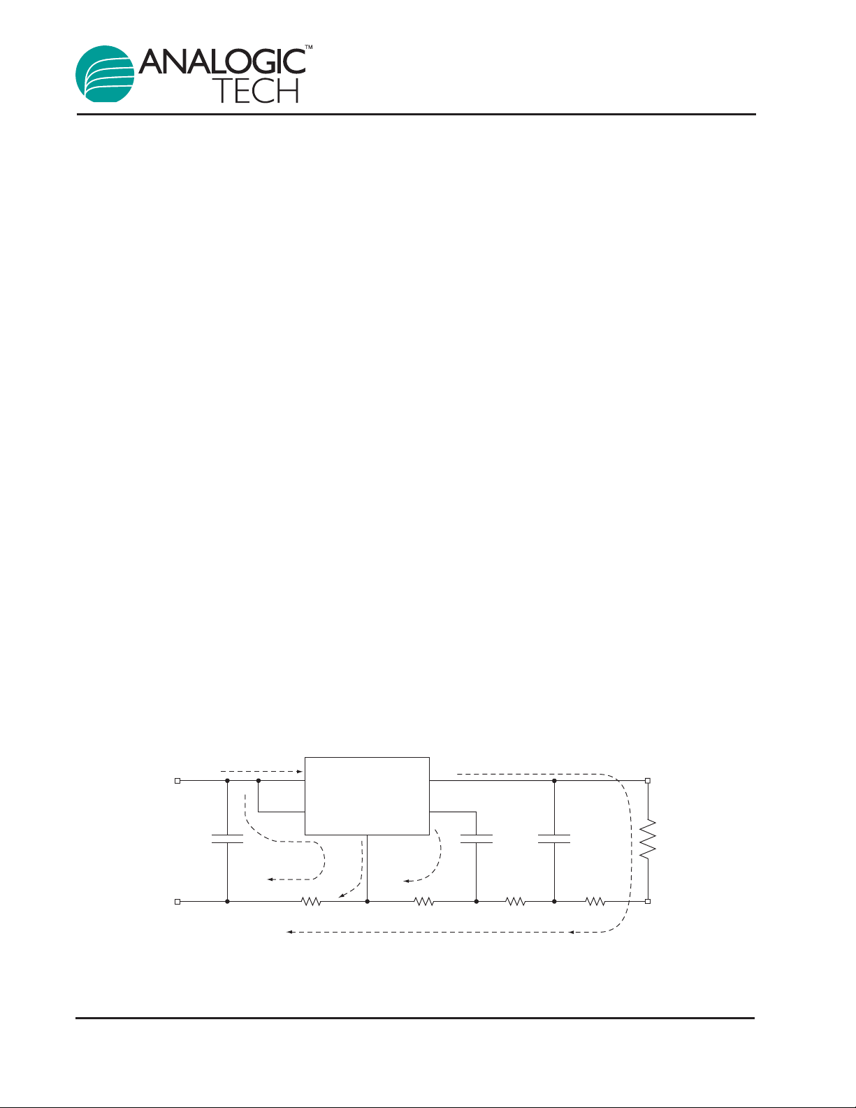
Figure 18 shows a common LDO regulator layout
scheme. The LDO Regulator, external capacitors
(CIN, C
connected to a common ground plane. This type of
layout will work in simple applications where good
power supply ripple rejection and low self noise are
not a design concern. For high performance applications, this method is not recommended.
OUT
and C
) and the load circuit are all
BYP
I
I
V
IN
IN
V
IN
LDO
V
LOAD
OUT
Regulator
EN
DC INPUT
GND
C
IN
I
RIPPLE
R
TRACE
I
LOAD
GND
I
GND
return + noise and ripple
Figure 18: Common LDO Regulator Layout with C
I
BYP
BYP
+ noise
R
TRACE
BYP
C
C
BYP
GND
LOOP
BYP
R
TRACE
Ripple feedback loop
C
R
OUT
TRACE
R
LOAD
12 3236.2001.11.0.9

AAT3236
300mA CMOS High Performance LDO
The problem with the layout in Figure 18 is the
bypass capacitor and output capacitor share the
same ground path to the LDO regulator ground pin
along with the high current return path from the load
back to the power supply. The bypass capacitor
node is connected directly to the LDO regulator
internal reference, making this node very sensitive
to noise or ripple. The internal reference output is
fed into the error amplifier, thus any noise or ripple
from the bypass capacitor will be subsequently
amplified by the gain of the error amplifier. This
effect can increase noise seen on the LDO regulator
output as well as reduce the maximum possible
power supply ripple rejection. There is PCB trace
impedance between the bypass capacitor connection to ground and the LDO regulator ground connection. When the high load current returns through
I
IN
V
I
RIPPLE
IN
Regulator
EN
I
GND
LDO
GND
V
IN
DC INPUT
C
IN
I
BYP
this path, a small ripple voltage is created, feeding
into the C
BYP
loop.
Figure 19 shows the preferred method for the
bypass and output capacitor connections. For low
output noise and highest possible power supply
ripple rejection performance, it is critical to connect
the bypass and output capacitor directly to the LDO
regulator ground pin. This method will eliminate
any load noise or ripple current feedback through
the LDO regulator.
Evaluation Board Layout
The AAT3236 evaluation layout follows the recommend printed circuit board layout procedures and
can be used as an example for good application
layouts.
Note: Board layout shown is not to scale.
I
LOAD
V
OUT
BYP
only
C
BYP
C
OUT
R
LOAD
GND
R
TRACE
I
return + noise and ripple
LOAD
R
TRACE
R
TRACE
R
TRACE
Figure 19: Recommended LDO Regulator Layout
Figure 20: Evaluation board Figure 21: Evaluation board Figure 22: Evaluation board
component side layout solder side layout top side silk screen layout /
assembly drawing
3236.2001.11.0.9 13

Ordering Information
AAT3236
300mA CMOS High Performance LDO
Output Voltage Package Marking
2.5V SOT-23-5 N/A AAT3236IGV-2.5-T1
2.7V SOT-23-5 N/A AAT3236IGV-2.7-T1
2.8V SOT-23-5 N/A AAT3236IGV-2.8-T1
2.85V SOT-23-5 N/A AAT3236IGV-2.85-T1
3.0V SOT-23-5 N/A AAT3236IGV-3.0-T1
3.3V SOT-23-5 N/A AAT3236IGV-3.3-T1
3.5V SOT-23-5 N/A AAT3236IGV-3.5-T1
2.5V SC70JW-8 N/A AAT3236IJS-2.5-T1
2.7V SC70JW-8 N/A AAT3236IJS-2.7-T1
2.8V SC70JW-8 N/A AAT3236IJS-2.8-T1
2.85V SC70JW-8 N/A AAT3236IJS-2.85-T1
3.0V SC70JW-8 N/A AAT3236IJS-3.0-T1
3.3V SC70JW-8 N/A AAT3236IJS-3.3-T1
3.5V SC70JW-8 N/A AAT3236IJS-3.5-T1
Bulk Tape and Reel
Part Number
14 3236.2001.11.0.9
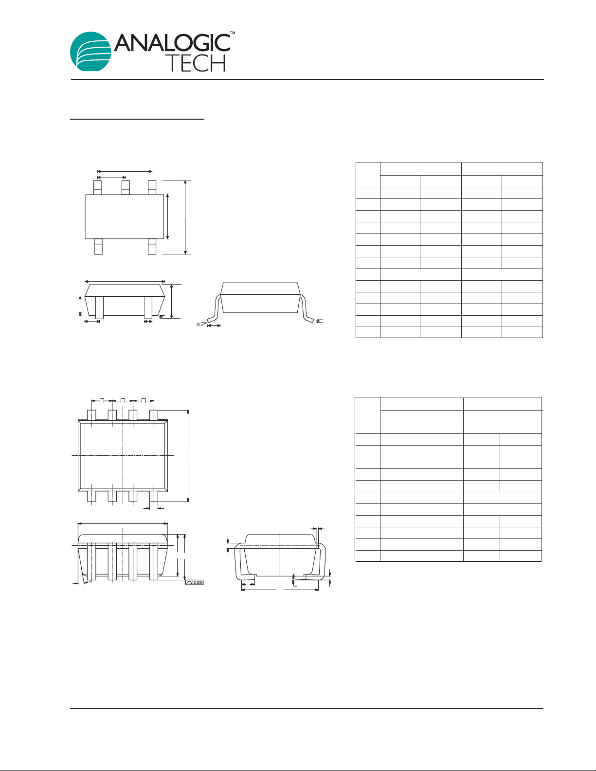
Package Information
SOT-23-5
AAT3236
300mA CMOS High Performance LDO
e
S1
Dim
Millimeters Inches
Min Max Min Max
A 1.00 1.30 0.039 0.051
A1 0.00 0.10 0.000 0.004
H
E
A2 0.70 0.90 0.028 0.035
b 0.35 0.50 0.014 0.020
c 0.10 0.25 0.004 0.010
D 2.70 3.10 0.106 0.122
E 1.40 1.80 0.055 0.071
D
e 1.90 0.075
H 2.60 3.00 0.102 0.118
A2
S
A
A1
b
L
c
L 0.37 0.015
S 0.45 0.55 0.018 0.022
S1 0.85 1.05 0.033 0.041
Θ 1° 9° 1° 9°
SC70JW-8
eee
Dim
Millimeters Inches
Min Max Min Max
E 2.10 BSC 0.083 BSC
E1 1.75 2.00 0.069 0.079
E
L 0.23 0.40 0.009 0.016
A 1.10 0.043
A1 0 0.10 0.004
A2 0.70 1.00 0.028 0.039
D 2.00 BSC 0.079 BSC
b
D
c
A2
A
0.048REF
e 0.50 BSC 0.020 BSC
b 0.15 0.30 0.006 0.012
c 0.10 0.20 0.004 0.008
Θ 08º08º
Θ1 4º 10º 4º 10º
Θ1
3236.2001.11.0.9 15
L
Θ
E1
A1

AAT3236
300mA CMOS High Performance LDO
This page intentionally left blank.
Advanced Analogic Technologies, Inc.
1250 Oakmead Parkway, Suite 310, Sunnyvale, CA 94086
Phone (408) 524-9684
Fax (408) 524-9689
16 3236.2001.11.0.9
 Loading...