


SmartSwitch
™
AAT4296/98
Five/Six Channel Push/Pull I/O Expander
4296.2006.12.1.3 1
General Description
The AAT4296/98 SmartSwitch is a member of
AnalogicTech's Application Specific Power MOSFET™ (ASPM™) product family. The AAT4296/98
is comprised of five/six push/pull output switches
that gate each respective output between a common
input supply and ground. This device is targeted for
I/O expansion applications, but can also be used for
a combination of general purposes to simplify power
switching with an off state load discharge.
The AAT4296/98 operates over an input voltage
range of 1.8V to 5.5V, making it ideal for batterypowered applications. The state of each output
channel is controlled with a single GPIO via the
EN/SET pin using AnalogicTech's Simple Serial
Control™ (S2Cwire™) interface. When EN/SET is
pulled to logic high, the device is enabled and consumes 3µA of typical quiescent current. In the off
state, each output is pulled low to ground to affect
a logic low state for I/O expander or power switching applications; this circuit will act as a load discharge function to rapidly turn off a load circuit.
Rated over the -40°C to +85°C temperature range,
the AAT4296 is offered in a Pb-free 8-pin SC70JW
package, and the AAT4298 is offered in both a Pbfree 10-pin SC70JW and a Pb-free 12-pin
TSOPJW package.
Features
•VINRange: 1.8V to 5.5V
• Independent Push/Pull Channels
— AAT4296: Five Channels
— AAT4298: Six Channels
• User-Programmable Interface
• Single GPIO Controls State of Each Output
• Optional Fast Auto-Discharge
• Low Quiescent Current: 3µA Typical
• Temperature Range: -40°C to +85°C
• Available in Pb-Free Packages:
— AAT4296: 8-Pin SC70JW
— AAT4298: 10-Pin SC70JW and
12-Pin TSOPJW
Applications
• Cell Phones
• Multiple Low Power Switching
• Personal Communication Devices
• Portable Electronic Devices
Typical Application
AAT4298
OUT1
OUT2
OUT3
OUT4
OUT5
OUT6
GND
OUT 1
OUT 2
OUT 3
OUT 4
OUT
5
OUT 6EN/SETEN/SET Input
VCC Input
VCC
查询AAT4296IJS-T1供应商
Pin Descriptions
Pin Configuration
AAT4296 AAT4298 AAT4298
SC70JW-8 SC70JW-10 TSOPJW-12
(Top View) (Top View) (Top View)
1
2
3
4
5
6
12
11
10
9
8
7
N/C
GND
OUT5
OUT4
OUT3
N/C
N/C
EN/SE
T
OUT1
OUT2
VCC
OUT6
EN/SET
OUT1
OUT2
VCC
OUT6
GND
N/C
OUT5
OUT4
OUT3
1
2
3
4
5
10
9
8
7
6
OUT2
OUT1
EN/SET
OUT3
OUT4
OUT5
GND
VCC
1
2
3
45
6
7
8
Pin #
AAT4298 AAT4298
AAT4296 SC70JW-10 TSOPJW-12 Symbol Function
1 7 8 VCC Input supply voltage.
2 8 9 OUT2 Channel 2 output pin.
3 9 10 OUT1 Channel 1 output pin.
4 10 11 EN/SET Input control pin using S
2
Cwire serial interface. The device
records rising edges of the clock and decodes them into 32
(AAT4296) or 64 (AAT4298) states controlling the ON/OFF
states of the outputs. See Table 1 for output settings. In addition, a logic low forces the device into shutdown mode, reducing the supply current to less than 1µA. This pin should not be
left floating.
5 1 2 GND Ground.
6 3 3 OUT5 Channel 5 output pin.
7 4 4 OUT4 Channel 4 output pin.
8 5 5 OUT3 Channel 3 output pin.
N/A 6 7 OUT6 Channel 6 output pin.
N/A 2 1, 6, 12 N/C Not connected.
AAT4296/98
Five/Six Channel Push/Pull I/O Expander
2 4296.2006.12.1.3
Absolute Maximum Ratings
1
Thermal Information
Symbol Description Value Units
θ
JA
Thermal Resistance
2
SC70JW-8, SC70JW-10 225
°C/W
TSOPJW-12 160
P
D
Maximum Power Dissipation
3
SC70JW-8, SC70JW-10 440
mW
TSOPJW-12 625
Symbol Description Value Units
VCCto GND Input to GND -0.3 to 6.0 V
OUTx to GND Output (Source) to GND -0.3 to VIN+ 0.3 V
EN/SET EN/SET to GND -0.3 to 6.0 V
T
J
Operating Junction Temperature Range -40 to +150 °C
AAT4296/98
Five/Six Channel Push/Pull I/O Expander
4296.2006.12.1.3 3
1. Stresses above those listed in Absolute Maximum Ratings may cause permanent damage to the device. Functional operation at conditions other than the operating conditions specified is not implied. Only one Absolute Maximum Rating should be applied at any one time.
2. Mounted on an FR4 board.
3. Derate 4.4mW/°C above 25°C.
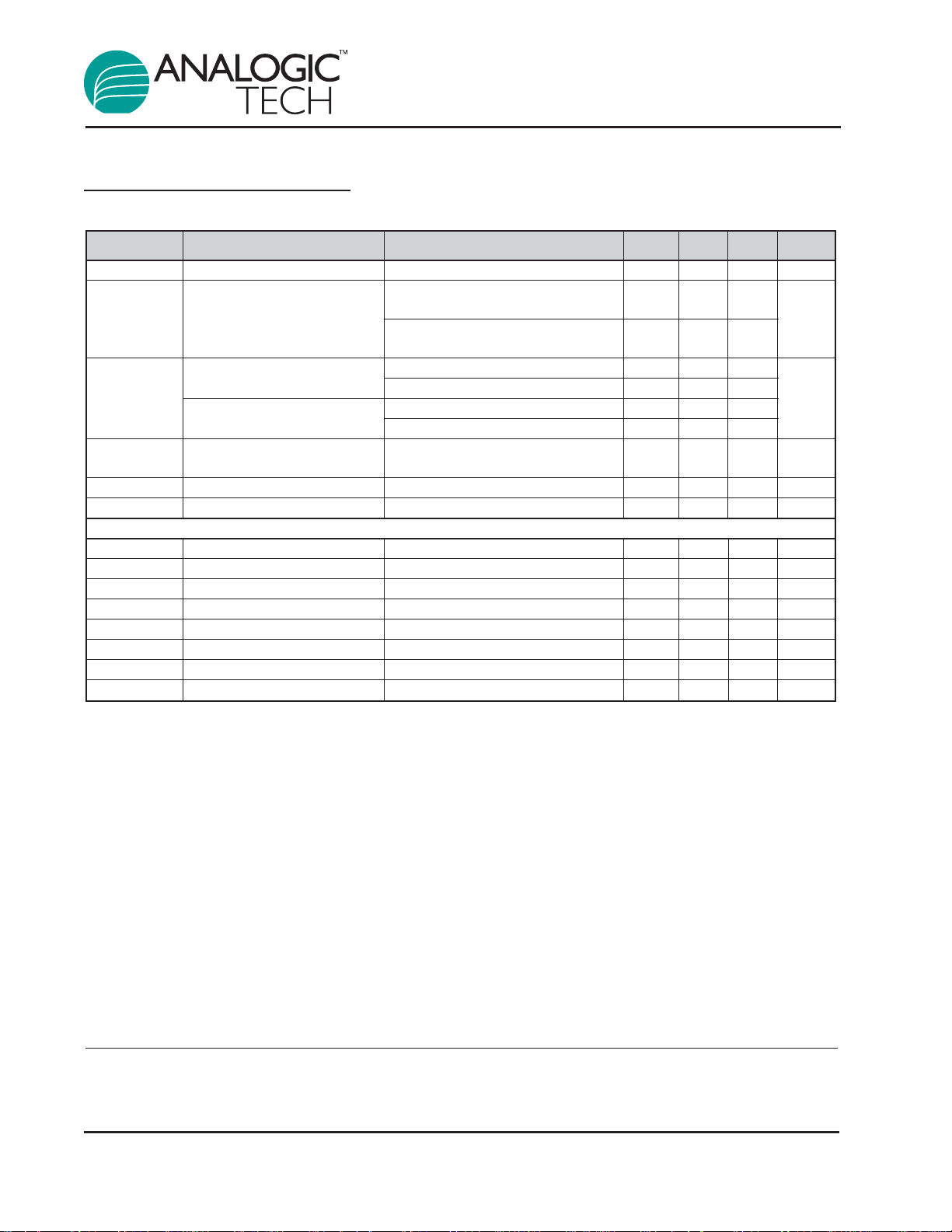
Electrical Characteristics
1
VCC= 5.0V; TA= -40°C to +85°C, unless otherwise noted. Typical values are TA= 25°C.
Symbol Description Conditions Min Typ Max Units
V
CC
Supply Voltage Range 1.8 5.5 V
I
Q
Quiescent Current
EN/SET = VCC= 5V, I
OUT
= 0, 3.0 10
µA
All Switches ON
EN/SET = GND, V
CC
= 5V, 1.0
OUTx = Open
On Resistance P-Channel
V
CC
= 5V 2.5 6.0
R
DS(ON)
VCC= 3.6V 3.0 7.0
Ω
On Resistance N-Channel
V
CC
= 5V 1.9 6.0
VCC= 3.6V 2.0 7.0
T
CRDS
On Resistance
2800 ppm/°C
Temperature Coefficient
T
ON
Output Turn-On Time
2
VCC= 5V, C
OUT
= 100nF; TA= 25°C 1.6 2.7 µs
T
OFF
Output Turn-Off Time
3
VCC= 5V, C
OUT
= 100nF; TA= 25°C 0.8 2.1 µs
EN/SET
V
EN(L)
Enable Threshold Low VIN= 1.8V 0.4 V
V
EN(H)
Enable Threshold High VIN= 5.5V 1.4 V
T
EN/SET LO
EN/SET Low Time 0.5 75 µs
T
EN/SET_HI_MIN
Minimum EN/SET High Time 50 ns
T
EN/SET_HI_MAX
Maximum EN/SET High Time 75 µs
T
OFF
EN/SET Off Timeout 500 µs
T
LAT
EN/SET Latch Timeout 500 µs
I
EN/SET
EN/SET Input Leakage -1 1 µA
AAT4296/98
Five/Six Channel Push/Pull I/O Expander
4 4296.2006.12.1.3
1. The AAT4296/98 is guaranteed to meet performance specifications over the -40°C to +85°C operating temperature range and is
assured by design, characterization, and correlation with statistical process controls.
2. T
ON
is the time after latch timeout to 90% of the output voltage. See Figure 1.
3. T
OFF
is the time after off timeout to 10% of the output voltage. See Figure 1.
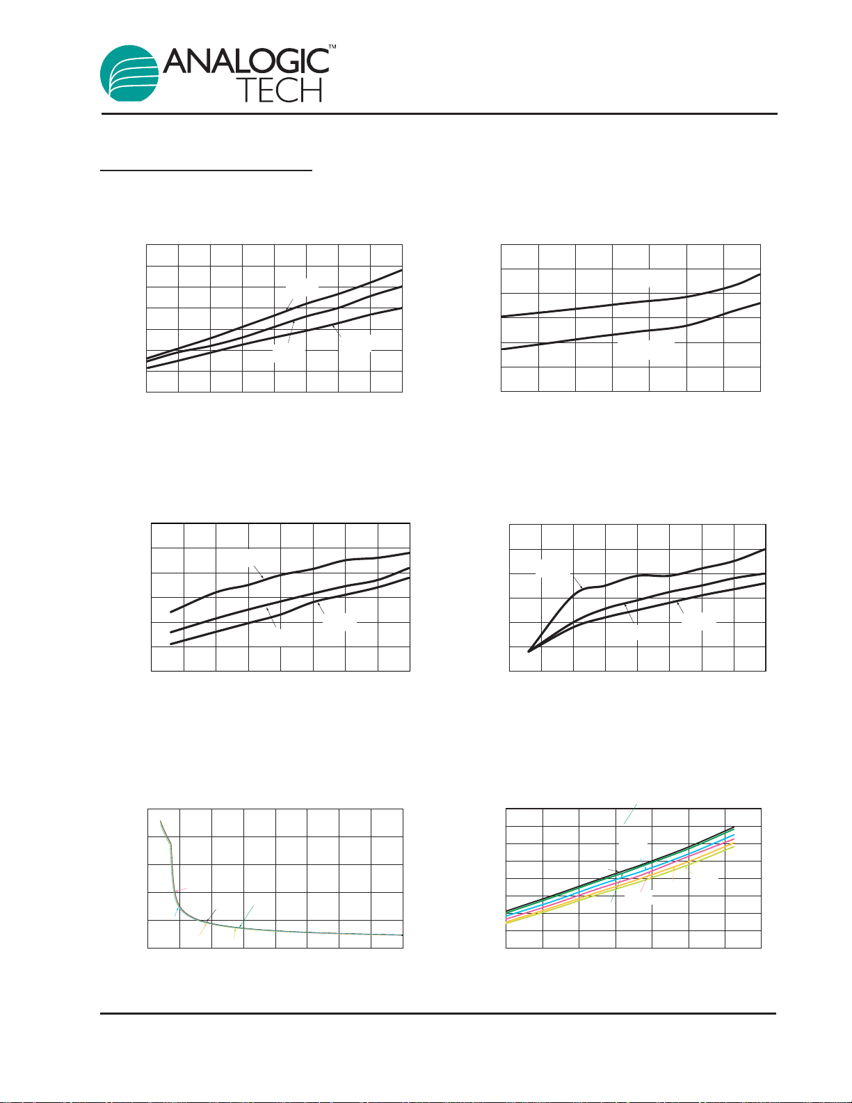
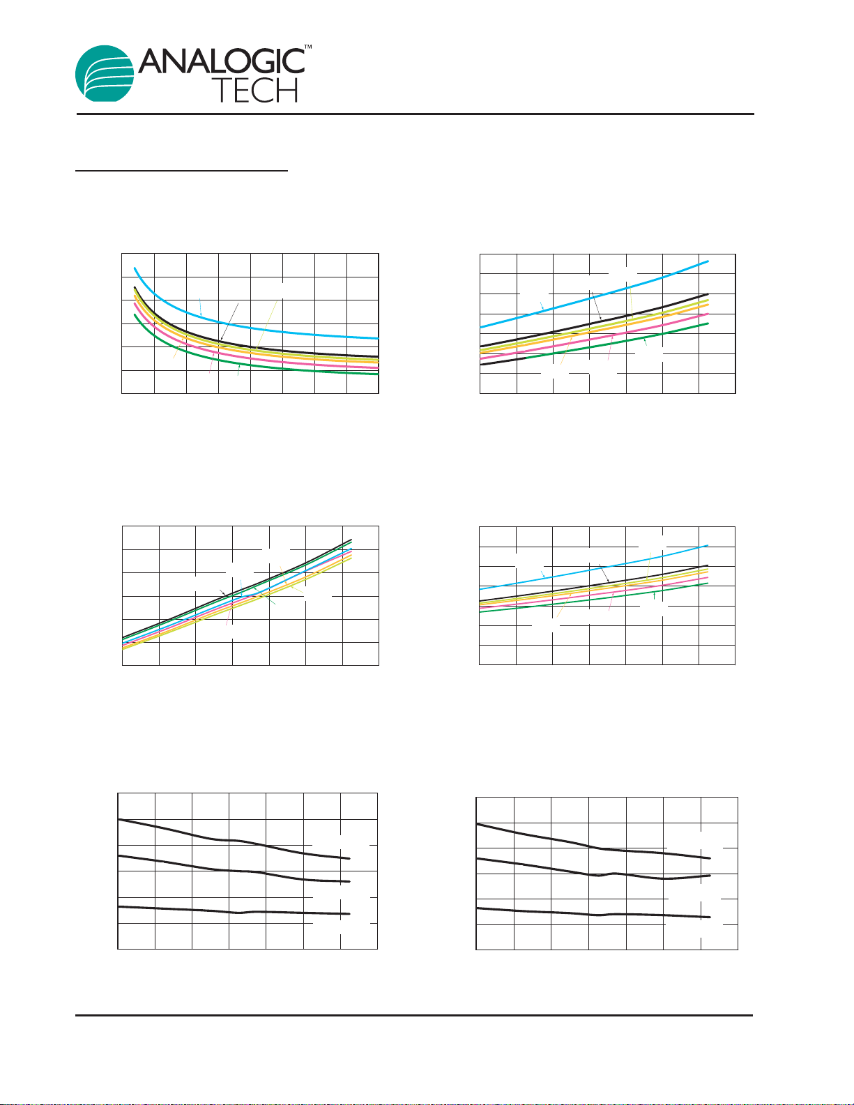
Typical Characteristics
Unless otherwise noted, VIN= 5V, CIN= 1µF, C
OUTx
= 0.1µF, TA= 25°C.
P-Channel R
DS(ON)
vs. Temperature
(I
LOAD
= 100mA)
Temperature (°
°
C)
R
DS(ON)
(
Ω
)
R
DS3
R
DS1
1.7
1.9
2.1
2.3
2.5
2.7
2.9
3.1
3.3
-40 -20 0 20 40 60 80 100
R
DS6
R
DS5
R
DS4
R
DS2
P-Channel R
DS(ON)
vs. Input Voltage
(I
LOAD
= 100mA)
Input Voltage (V)
R
DS(ON)
(Ω
Ω
)
0
5
10
15
20
25
1.5 2.0 2.5 3.0 3.5 4.0 4.5 5.0 5.5
R
DS1
R
DS2
R
DS6
R
DS5
R
DS4
R
DS3
VIL vs. Input Voltage
Input Voltage (V)
V
IL
(V)
0.4
0.5
0.6
0.7
0.8
0.9
1.0
1.5 2.0 2.5 3.0 3.5 4.0 4.5 5.0 5.
5
85°C
25°C
-40°C
VIH vs. Input Voltage
Input Voltage (V)
V
IH
(V)
0.6
0.7
0.8
0.9
1.0
1.1
1.2
1.5 2.0 2.5 3.0 3.5 4.0 4.5 5.0 5.5
85°C
25°C
-40°C
Quiescent Current vs. Temperature
Temperature (°°C)
Quiescent Current (
μ
A)
0.5
1.0
1.5
2.0
2.5
3.0
3.5
-40 -20 0 20 40 60 80 100
VCC = 5.0V
V
CC
= 3.6V
Quiescent Current vs. Input Voltage
Input Voltage (V)
Quiescent Current (μ
μ
A)
0.0
0.5
1.0
1.5
2.0
2.5
3.0
3.5
1.5 2 2.5 3 3.5 4 4.5 5 5.5
85°C
25°C
-40°C
AAT4296/98
Five/Six Channel Push/Pull I/O Expander
4296.2006.12.1.3 5
Typical Characteristics
Unless otherwise noted, VIN= 5V, CIN= 1µF, C
OUTx
= 0.1µF, TA= 25°C.
EN/SET Off Timeout vs. Temperature
Temperature (°C)
Off Timeout, T
OFF
(μs)
50
100
150
200
250
300
350
-40 -20 0 20 40 60 80 100
V
CC
= 3.3V
V
CC
= 1.8V
V
CC
= 5.0V
EN/SET Latch Timeout vs. Temperature
Temperature (°C)
Latch Timeout, T
LAT
(µs)
50
100
150
200
250
300
350
-40 -20 0 20 40 60 80 100
V
CC
= 5.0V
V
CC
= 3.3V
V
CC
= 1.8V
N-Channel R
DS(ON)
vs. Temperature
(VCC = 3.6V; I
LOAD
= 100mA)
Temperature (°
°
C)
R
DS(ON)
(
Ω
)
0.0
0.5
1.0
1.5
2.0
2.5
3.0
3.5
-40 -20 0 20 40 60 80 100
R
DS6
R
DS5
R
DS2
R
DS1
R
DS3
R
DS4
P-Channel R
DS(ON)
vs. Temperature
(VCC = 3.6V; I
LOAD
= 100mA)
Temperature (°
°
C)
R
DS(ON)
(
Ω
)
2.2
2.5
2.8
3.1
3.4
3.7
4.0
-40 -20 0 20 40 60 80 100
R
DS1
R
DS4
R
DS2
R
DS5
R
DS3
R
DS6
N-Channel R
DS(ON)
vs. Temperature
(I
LOAD
= 100mA)
Temperature (°
°
C)
R
DS(ON)
(
Ω
)
0.8
1.1
1.4
1.7
2.0
2.3
2.6
2.9
-40 -20 0 20 40 60 80 100
R
DS6
R
DS3
R
DS4
R
DS5
R
DS2
R
DS1RDS1
N-Channel R
DS(ON)
vs. Input Voltage
(I
LOAD
= 100mA)
Input Voltage (V)
R
DS(ON)
(Ω
Ω
)
1.0
1.5
2.0
2.5
3.0
3.5
4.0
1.5 2.0 2.5 3.0 3.5 4.0 4.5 5.0 5.5
R
DS6
R
DS5
R
DS2
R
DS1
R
DS3
R
DS4
AAT4296/98
Five/Six Channel Push/Pull I/O Expander
6 4296.2006.12.1.3
Typical Characteristics
Unless otherwise noted, VIN= 5V, CIN= 1µF, C
OUTx
= 0.1µF, TA= 25°C.
Turn-On Characteristic
(R
LOAD1
= R
LOAD2
= 100ΩΩ; C
OUT1
= C
OUT2
= 0.1μF)
Time (50
μ
s/div)
EN/SET
(5V/div)
V
OUT1
(5V/div)
V
OUT2
(5V/div)
0V
5V
5V
0V
5V
0V
Turn-On Characteristic
(R
LOAD1
= R
LOAD2
= 100ΩΩ; C
OUT1
= C
OUT2
= 0.1μF)
Time (50
μ
s/div)
EN/SET
(5V/div)
V
OUT1
(5V/div)
V
OUT2
(5V/div)
0V
5V
5V
0V
5V
0V
Turn-On Characteristic
(R
LOAD1
= R
LOAD2
= 100ΩΩ; C
OUT1
= C
OUT2
= 0.1μF)
Time (50
μ
s/div)
EN/SET
(5V/div)
V
OUT1
(5V/div)
V
OUT2
(5V/div)
0V
5V
5V
0V
5V
0V
Turn-On Characteristic
(R
LOAD1
= R
LOAD2
= 100ΩΩ; C
OUT1
= C
OUT2
= 0.1μF)
Time (50
μ
s/div)
EN/SET
(5V/div)
V
OUT1
(5V/div)
V
OUT2
(5V/div)
0V
5V
5V
0V
5V
0V
Turn-On and Turn-Off Time
vs. Temperature
Temperature (°°C)
Time (
μ
s)
0.0
0.4
0.8
1.2
1.6
2.0
-40 -20 0 2 0 40 60 80 100
TON (Rise Time)
T
OFF
(Fall Time)
EN/SET Timeout vs. Input Voltage
Input Voltage (V)
Timeout (
μ
s)
80
110
140
170
200
230
260
290
1.5 2 2.5 3 3.5 4 4.5 5 5.5
T
LATCH
T
OFF
AAT4296/98
Five/Six Channel Push/Pull I/O Expander
4296.2006.12.1.3 7

Typical Characteristics
Unless otherwise noted, VIN= 5V, CIN= 1µF, C
OUTx
= 0.1µF, TA= 25°C.
Time (50µs/div)
EN/SET
(5V/div)
V
OUT1
(5V/div)
V
OUT2
(100mV/div,
AC coupled)
Turn-On Transient Characteristic
(R
LOAD1
= R
LOAD2
= 100Ω; C
OUT1
= C
OUT2
= 0.1µF)
0V
5V
5V
0V
5V
Transition of Outputs
(R
LOAD1
= R
LOAD2
= 100Ω; C
OUT1
= C
OUT2
= 0.1µF)
Time (50µs/div)
EN/SET
(5V/div)
V
OUT1
(5V/div)
V
OUT2
(5V/div)
0V
5V
5V
0V
5V
0V
Turn-Off Characteristic
(R
LOAD1
= R
LOAD2
= 100ΩΩ; C
OUT1
= C
OUT2
= 0.1μF)
Time (50
μ
s/div)
EN/SET
(5V/div)
V
OUT1
(5V/div)
V
OUT2
(5V/div)
0V
5V
5V
0V
5V
0V
AAT4296/98
Five/Six Channel Push/Pull I/O Expander
8 4296.2006.12.1.3

AAT4296/98
Five/Six Channel Push/Pull I/O Expander
4296.2006.12.1.3 9
Functional Description
The AAT4296/98 is comprised of five/six push/pull
output slew rate limited load switches primarily targeted for microcontroller general purpose
input/output (I/O) expansion applications. Each
push/pull output is supplied by the common V
CC
input and is controlled via the digital EN/SET input
pin. When a given output is enabled, the voltage
source applied to the VCC pin is then switched to
the respective output. The high-side P-channel
MOSFET transistor has a typical on resistance
(R
DS(ON)
) of 3Ω when operating from a 3.6V supply.
When a respective output is disabled or turned off,
the given output pin is then connected to ground
through a low side N-channel MOSFET with a typical on resistance (R
DS(ON)
) of 2Ω. This circuit architecture affects a simple logic control with the high
level based on the applied VCC. For the AAT4296,
this creates a 1-to-5 I/O expander, and for the
AAT4298 this creates a 1-to-6 I/O expander. Both
the AAT4296 and AAT4298 have been designed to
operate with an input voltage range of 1.8V to 5.5V,
making them ideal for battery-powered applications.
Functional Block Diagram
VCC
GND
OUT1
AAT4298
OUT2
OUT3
OUT4
OUT5
EN/SET
S
2
Cwire
Serial
Interface
OUT6

These devices may also be used for load switching
applications, as well as I/O expansion. Since the
VCCis gated to each output through a slew rate limited low on-resistance switch, they are ideal for
controlling applications circuits with light load current requirements. Such applications could include
simple LED function indicator lamps, RGB LED
fashion lighting, audio and RF circuits, or any other
system with a power requirement that does not
exceed the thermal dissipation limits of the load
switch and device package.
Each device push/pull output may be represented
by the following circuit and simplified equivalent
model (Figures 1 and 2):
Figure 1: Push/Pull Output Circuit.
Figure 2: Simplified Equivalent Model.
The state of each output is controlled via the
EN/SET pin using AnalogicTech's S
2
Cwire interface. To enable a respective switch, a series of
clocked pulses should be applied to the EN/SET
pin. The number of pulses clocked will determine
the switch configuration based on the truth table
shown in Table 1. At the end of the serial pulse
data set, the EN/SET set pin should be held high
to then latch the clocked data and enable the
desired switch configuration. When the device is
enabled with the EN/SET held to a logic high state,
the device quiescent current consumption will typically increase to 3µA and normal ambient room
temperatures. If output sequencing of the switches
is not necessary, all of the outputs will be switched
on simultaneously on the first rising edge of the
EN/SET pin by simply pulling the EN/SET to a
logic high level. The default switch position for
one clock pulse is all switches "on." However, if
output sequencing is desired, a series of pulses on
the EN/SET pin will set the outputs to the desired
state (refer to Table 1 for output settings).
The AAT4296/98 offers two different options when
the switches are in the off state. For applications
with an active pull down or auto-discharge
requirement, the internal N-channel switch will
connect the output node to ground with a series
resistance of 2Ω.
S2Cwire Serial Interface
The ON/OFF state of the output is controlled by the
EN/SET serial data input. An internal control
counter is clocked on the rising edge of the
EN/SET pin and is decoded into the 32/64 possible
states (see Table 1).
3Ω
2Ω
V
CC
Control
OUT
OUT
V
CC
Control
AAT4296/98
Five/Six Channel Push/Pull I/O Expander
10 4296.2006.12.1.3

Table 1: Output Settings.
AAT4298 AAT4298
AAT4296 (only)
Clock OUT6 OUT5 OUT4 OUT3 OUT2 OUT1 Clock OUT6 OUT5 OUT4 OUT3 OUT2 OUT1
1 on on on on on on 33 off on on on on on
2 on on on on on off 34 off on on on on off
3 on on on on off on 35 off on on on off on
4 on on on on off off 36 off on on on off off
5 on on on off on on 37 off on on off on on
6 on on on off on off 38 off on on off on off
7 on on on off off on 39 off on on off off on
8 on on on off off off 40 off on on off off off
9 on on off on on on 41 off on off on on on
10 on on off on on off 42 off on off on on off
11 on on off on off on 43 off on off on off on
12 on on off on off off 44 off on off on off off
13 on on off off on on 45 off on off off on on
14 on on off off on off 46 off on off off on off
15 on on off off off on 47 off on off off off on
16 on on off off off off 48 off on off off off off
17 on off on on on on 49 off off on on on on
18 on off on on on off 50 off off on on on off
19 on off on on off on 51 off off on on off on
20 on off on on off off 52 off off on on off off
21 on off on off on on 53 off off on off on on
22 on off on off on off 54 off off on off on off
23 on off on off off on 55 off off on off off on
24 on off on off off off 56 off off on off off off
25 on off off on on on 57 off off off on on on
26 on off off on on off 58 off off off on on off
27 on off off on off on 59 off off off on off on
28 on off off on off off 60 off off off on off off
29 on off off off on on 61 off off off off on on
30 on off off off on off 62 off off off off on off
31 on off off off off on 63 off off off off off on
32 on off off off off off 64 off off off off off off
AAT4296/98
Five/Six Channel Push/Pull I/O Expander
4296.2006.12.1.3 11

AAT4296/98
Five/Six Channel Push/Pull I/O Expander
12 4296.2006.12.1.3
The S2Cwire interface relies on the number of rising edges of the EN/SET pin to address and load
the registers. S2Cwire latches data or address
after the EN/SET pin has been held high for time
T
LAT
. The interface records rising edges of the
EN/SET pin and decodes them into 32 (for
AAT4296) or 64 (for AAT4298) different states, as
indicated in Table 1. There are 32 (for AAT4296)/
64 (for AAT4298) different sequences for controlling individual turn-on/turn-off of each switch. The
counter can be clocked at speeds up to 1MHz,
such that intermediate states are not visible.
Alternatively, the EN/SET clock pulses may be
entered one at a time for desired setting. The first
rising edge of EN/SET enables the IC and turns all
the switches ON. Once the final clock cycle is
received, the EN/SET pin is held high to maintain
the device setting. The device is disabled 500µs
(T
OFF
) after the EN/SET pin transitions to a logic
low state.
Figure 3: Timing Diagram.
OUTn
T
H
T
L
T
LAT
T
ON
TOT
OFF
EN/SET
Applications Information
The AAT4296 and AAT4298 have been designed
so that no external parts are required for the device
to function as a general purpose I/O expander.
Such external parts could include bypass capacitors, or pull-up or pull-down resistors.
For applications which may use some or all of the
output to switch light load current levels to application circuits, good engineering practice would dictate the use of small bypass capacitors place on
the VCCinput and each output which is being used
to conduct current to a load. The use of small
ceramic capacitors between the input and output
nodes to ground will aid in reducing line and load
transient response effects. Refer to the application
schematic of Figure 4 for an example for placing
bypass capacitors.
Input Capacitor
Typically a 0.1µF to 1µF capacitor is recommended for CINin most applications. A CINcapacitor is
not required for basic operation; however, CINis
useful in preventing load transient effects from
affecting upstream circuits when internal switches
are enabled to their respective output load circuits.
C
IN
should be located as close to the device VINpin
as practically possible.
There is no specific capacitor equivalent series
resistance (ESR) requirement for CIN; however, for
higher current operation, ceramic capacitors are recommended for CIN due to their inherent capability
over tantalum or aluminum electrolytic capacitors to
withstand input current surges from low impedance
sources, such as batteries in portable devices.
Output Capacitor
For typical applications where the AAT4696/98 is
used for I/O expansion, no output capacitors are
required. Many other common applications such
as controlling LED indicator lamps in portable products do not require an output capacitor because
the end load is not sensitive to device turn-on transient effects.
For improved load transient response in systems
using the AAT4296/98 for load switching, the addition of a small output capacitor placed between the
output pins and ground can have a beneficial
effect. A 0.1µF ceramic capacitor is suggested as
a reasonable value for an output capacitor. Please
refer to Figure 4.

Applications Circuit
Figure 4: Typical Application Diagram.
AAT4298
OUT1
OUT2
OUT3
OUT4
OUT5
OUT6
GND
C1* C2* C3* C4* C5* C6*
OUT 1
OUT 2
OUT 3
OUT 4
OUT 5
OUT 6EN/SETEN/SET Input
VCC Input
VCC
AAT4296/98
Five/Six Channel Push/Pull I/O Expander
4296.2006.12.1.3 13
The output capacitor has no specific capacitor type
or ESR requirement. If desired, C
OUT
may be
increased to a value greater than 0.1µF without
limit to accommodate any load transient condition
without adversely affecting the device turn-on slew
rate time.
Thermal Considerations
The AAT4296 and AAT4298 are designed to deliver continuous output load currents. The limiting
characteristic for maximum safe operating output
load current is package power dissipation. In order
to obtain high operating currents, careful device
layout and circuit operating conditions need to be
taken into account.
At any given ambient temperature (TA), the maximum package power dissipation can be determined by the following equation:
Constants for the AAT4296 and AAT4298 are maximum junction temperature, T
J(MAX)
= 125°C, and
package thermal resistance, θJA= 120°C/W. Worstcase conditions are calculated at the maximum
operating temperature, where TA= 85°C. Typical
conditions are calculated under normal ambient
conditions, where TA= 25°C.
At 25°C ambient, the AAT4296 is capable of dissipating 440mW of power. If all five channels have
5.0V output, the average current is 121mA per
channel. The AAT4298 is capable of dissipating
625mW of power. If all six channels have 5.0V output, the average current is 131.5mA per channel.
At 85°C ambient, the AAT4296 is capable of dissipating 177.78mW of power. If all five channels
have 5.0V output, the average current is 76.5mA
per channel. The AAT4298 is capable of dissipating 250mW of power. If all six channels have 5.0V
output, the average current is 83mA per channel.
P
D(MAX)
=
T
J(MAX)
- T
A
θ
JA
*Use of capacitors on each output is optional.

AAT4296/98
Five/Six Channel Push/Pull I/O Expander
14 4296.2006.12.1.3
Figure 5: Infrared, Bluetooth, RGB, and Backlighting Control.
IN
EN/SET
OUT2
GND
OUT6
OUT5
OUT4
OUT3
OUT1
AAT4296
RG B
5V
A series of
pulses
Bluetooth
Device
EN
Infrared
Device
EN
Backlighting
Driving LED Loads
The AAT4296 and AAT4298 can be used to drive
LEDs or other applications with light load current
requirements. LED applications may include main
and sub-LCD display backlighting, camera photoflash applications, color (RGB) LEDs, and infrared
(IR) diodes for remotes. In series with LEDs, ballast resistors must be used to limit the LED current.
The LED current will vary with supply voltage and
LED forward voltage. Most types of LEDs have forward voltage specifications ranging from 2.0V to
5.0V. Calculate the necessary ballast resistor value
from the following formula:
Where:
R
LED
is the resistance of resistor to be placed in
series with the LED (Ω).
VINis the input supply voltage to the device (V).
VFis the forward voltage of the LED (V).
R
DS(ON)
is the resistance of the switch when it is
turned on (Ω).
I
LED
is the desired operating current of the LED (A).
R
LED
= - R
DS(ON
)
(VIN - VF)
I
LED
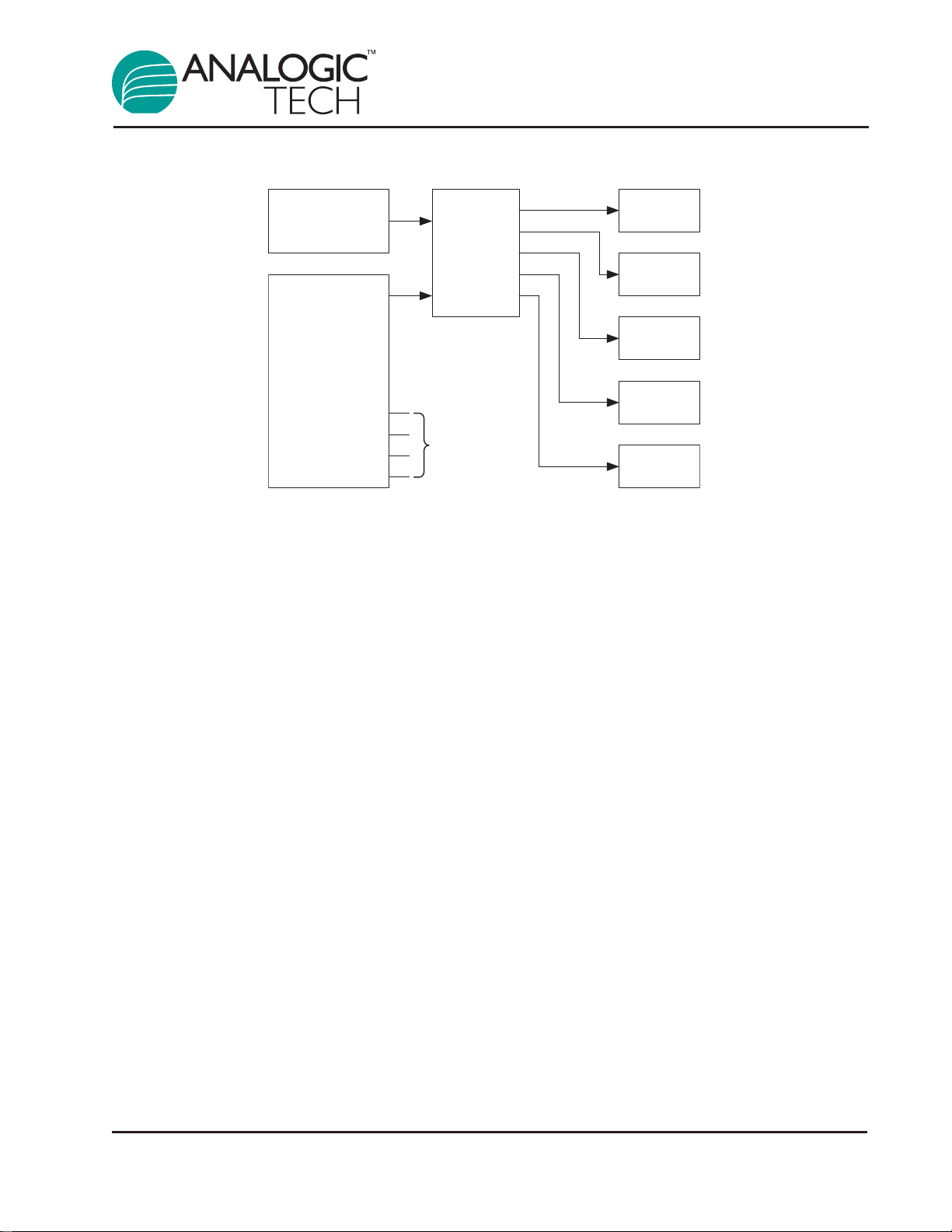
Figure 6: GPIO I/O Expander (Condense Five GPIO Control Lines to One Using AAT4296).
Circuit 1
30mA
Circuit 2
30mA
Circuit 3
30mA
Circuit 4
30mA
Circuit 5
30mA
System
µController
GPIO 1
GPIO 2
GPIO 3
GPIO 4
GPIO 5
VIN
VIN
VIN
VIN
VIN
GPIO 2
to
GPIO 5
are now free for
other uses
IN
OUT1
OUT2
OUT3
OUT4
OUT5
AAT4296
Low Dropout
Voltage
Regulator
EN/SET
AAT4296/98
Five/Six Channel Push/Pull I/O Expander
4296.2006.12.1.3 15

AAT4296/98
Five/Six Channel Push/Pull I/O Expander
16 4296.2006.12.1.3
Ordering Information
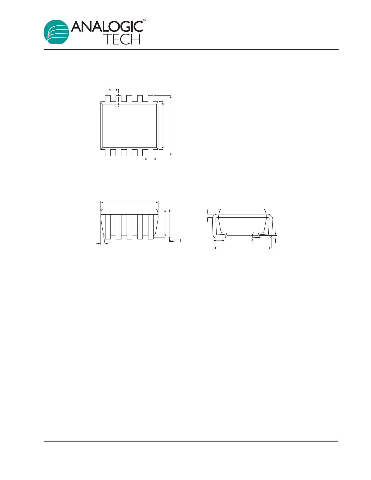
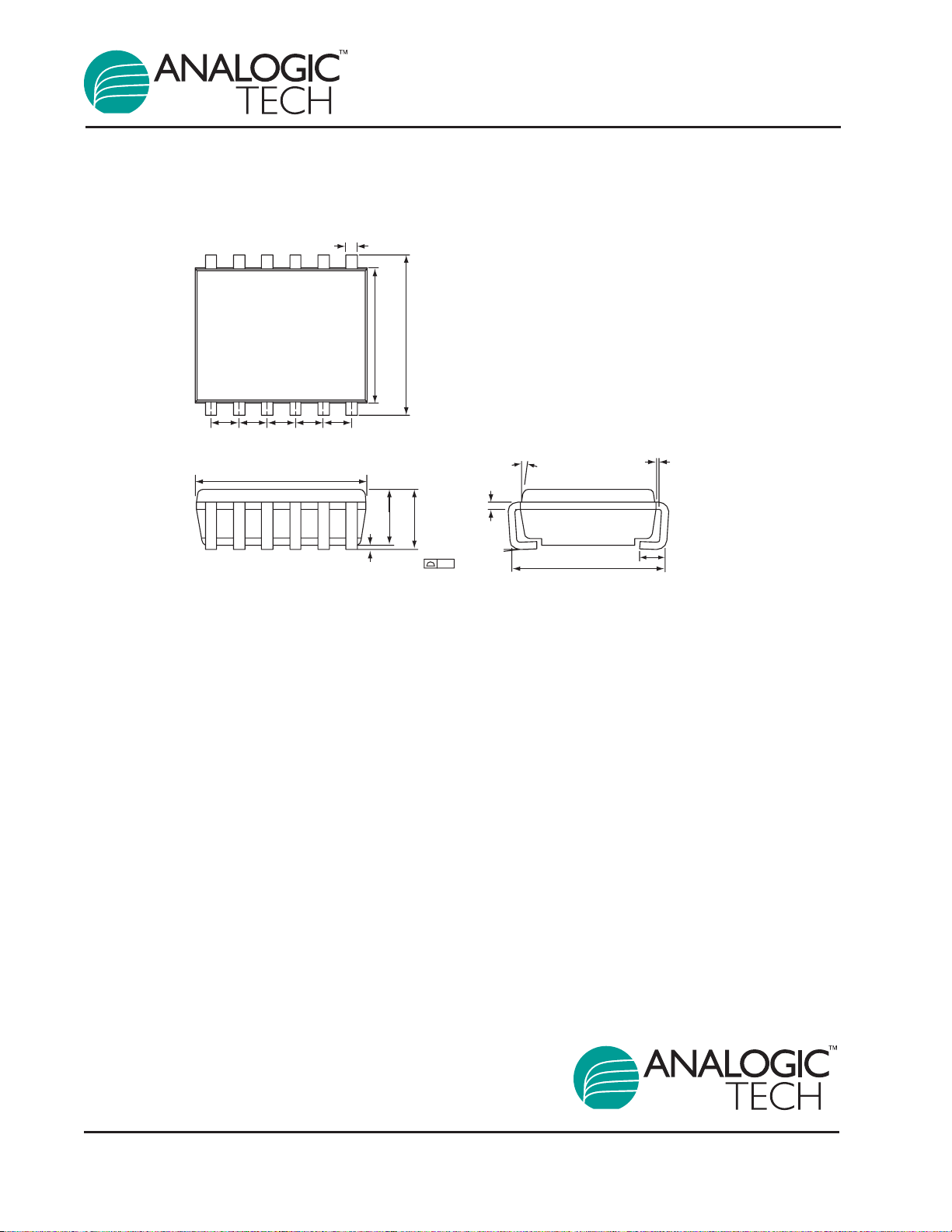
Package Information
SC70JW-8
All dimensions in millimeters.
0.225 ± 0.075
0.45
±
0.10
0.05
±
0.05
2.10 ± 0.30
2.00
±
0.20
7
° ± 3°
4° ± 4
°
1.75
±
0.10
0.85
±
0.15
0.15
±
0.05
1.10 MAX
0.100
2.20
±
0.20
0.048REF
0.50 BSC 0.50 BSC 0.50 BSC
All AnalogicTech products are offered in Pb-free packaging. The term “Pb-free” means
semiconductor products that are in compliance with current RoHS standards, including
the requirement that lead not exceed 0.1% by weight in homogeneous materials. For more
information, please visit our website at http://www.analogictech.com/pbfree.
Package Marking
1
Part Number (Tape and Reel)
2
SC70JW-8 QIXYY AAT4296IJS-T1
SC70JW-10 AAT4298IJQ-T1
TSOPJW-12 QEXYY AAT4298ITP-T1
1. XYY = assembly and date code.
2. Sample stock is generally held on part numbers listed in BOLD.
AAT4296/98
Five/Six Channel Push/Pull I/O Expander
4296.2006.12.1.3 17
SC70JW-10
All dimensions in millimeters.
0.45 ± 0.10
0.05
±
0.05
2.10 ± 0.30
4
° ± 4°
0.15
±
0.05
2.00 ± 0.20
7
° ± 3°
0.85
±
0.15
1.10 MAX
0.100
0.225 ± 0.075
1.75
±
0.10
2.20
±
0.20
0.40 BSC
Top View
Side View End View
TSOPJW-12
All dimensions in millimeters.
0.20
+ 0.10
- 0.05
0.055 ± 0.045
0.45 ± 0.15
7° NOM
4° ± 4°
3.00 ± 0.10
2.40 ± 0.10
2.85 ± 0.20
0.50 BSC 0.50 BSC 0.50 BSC 0.50 BSC 0.50 BSC
0.15 ± 0.05
0.9625
±
0.0375
1.00
+ 0.10
- 0.065
0.04 REF
0.010
2.75 ± 0.25
AAT4296/98
Five/Six Channel Push/Pull I/O Expander
18 4296.2006.12.1.3
Advanced Analogic Technologies, Inc.
830 E. Arques Avenue, Sunnyvale, CA 94085
Phone (408) 737-4600
Fax (408) 737-4611
AnalogicTech cannot assume responsibility for use of any circuitry other than circuitry entirely embodied in an AnalogicTech product. No circuit patent licenses, copyrights, mask work
rights, or other intellectual property rights are implied.
AnalogicTech reserves the right to make changes to their products or specifications or to discontinue any product or service without notice, and advise customers to obtain the latest
version of relevant information to verify, before placing orders, that information being relied on is current and complete. All products are sold subject to the terms and conditions of sale
supplied at the time of order acknowledgement, including those pertaining to warranty, patent infringement, and limitation of liability.
AnalogicTech warrants performance of its semiconductor products to the specifications applicable at the time of sale in accordance with AnalogicTech’s standard warranty. Testing and
other quality control techniques are utilized to the extent AnalogicTech deems necessary to support this warranty. Specific testing of all parameters of each device is not necessarily
performed.
 Loading...