


查询AAT3560IGY-220-T1供应商
AAT3560/2/4
NanoPower Voltage Detector
General Description
The AAT3560 Series of PowerManager™ products
is a member of AATI's Total Power Management
IC™ (TPMIC™) product family. These voltage
detectors are ideal for monitoring voltage supplies
in portable systems, where extended battery life is
critical. They provide a low cost, reliable solution by
eliminating several external components. The
AAT3560 series operates by monitoring the system
power supply voltage. When the input voltage
drops below a fixed threshold, the device output
changes state depending upon configuration.
When the input voltage rises above the threshold,
the device output reverts back to the previous
state. The AAT3560 series are available with three
different output stages: AAT3560 push-pull active
high output, AAT3562 push-pull active low output
and AAT3564 open drain active low output.
The quiescent supply current is extremely low, typically 1µA , making it ideal for portable battery operated equipment.
The AAT3560/2/4 are available in a 3 pin SOT-23
package and are specified over -40 to 85°C operating temperature range..
PowerManager
™
Features
• 1.2V to 5.5V Input voltage range
• Operates down to 1.2V
• Extremely low quiescent current: less than 2µA
• High accuracy detection threshold: ±1.5%
• Monitor Power Supply Voltages
• Fixed thresholds from 2.2V to 4.6V
• Available output configurations:
• Open-drain output
• CMOS active high output
• CMOS active low output
• Temp range -40 to 85°C
• 3 pin SOT-23 package
Applications
• Portable Electronics
• Battery Packs
• Battery Charger Circuits
• Data Acquisition Systems
• Power Supplies
• Notebook Computers
• Intelligent Instruments
Preliminary Information
Typical Application
DC/DC
Converter
V
CC
µP
+
Li Ion
3560.2002.3.0.91 1
V
CC
AAT3560
AAT3562
AAT3564
GND
RESET
(RESET)
SUSPEND

NanoPower Voltage Detector
Pin Descriptions
AAT3560, 3562, 3564 (SOT23-3)
Pin # Symbol Function
1 GND Ground
2 RESET (RESET) Reset output. See table below for output configurations.
3VCCSupply Voltage (+1.2V to +5.5V)
Part Number Descriptions
SOT23-3 Part Number Part Description
AAT3560 RESET Push Pull Active High
AAT3562 RESET Push Pull Active Low
AAT3560/2/4
AAT3564 RESET Open Drain, Active Low
Pin Configuration
GND
(RESET) RESET
3-Pin SOT23
(Top View)
1
3
2
V
CC
2 3560.2002.3.0.91
AAT3560/2/4
NanoPower Voltage Detector
Absolute Maximum Ratings (T
=25°C unless otherwise noted)
A
Symbol Description Value Units
V
CC
V
RESET
I
MAX
I
RESET
T
J
T
LEAD
Note: Stresses above those listed in Absolute Maximum Ratings may cause permanent damage to the device. Functional operation at conditions other than the operating conditions specified is not implied. Only one Absolute Maximum rating should be applied at any one time.
VCCto GND -0.3 to 5.5 V
RESET to GND (Push-Pull Output) -0.3 to VCC+0.3
RESET to GND (Open Drain Output) -0.3 to 5.5
V
Maximum Continuous Input Current 20 mA
RESET/RESET Current 20 mA
Operating Junction Temperature Range -40 to 150 °C
Maximum Soldering Temperature (at Leads) for 10s 300 °C
Thermal Information
Symbol Description Value Units
Θ
JA
P
D
Note 1: Mounted on FR4 board.
Electrical Characteristics (V
Maximum Thermal Resistance
Maximum Power Dissipation
= 5V, TA= -40 to 85°C unless otherwise noted. Typical values
IN
are at TA=25°C, ,VCC= 5V for 4.63/4.38V versions, VCC= 3.3V for 3.08/2.93V versions, VCC= 3.0V for 2.63V
version and VCC= 2.5V for 2.32/2.2V versions )
1
1
200 °C/W
320 mW
Symbol Description Conditions Min Typ Max Units
T
= 0 to 70ºC 1.0 5.5
V
V
Operation Voltage
CC
I
Quiescent Current
Q
RESET Threshold (Table 1)
TH
dVTH/ºC RESET Threshold Tempco 40 ppm/°C
V
V
V
RESET Low Output Voltage RESET asserted
OL
AAT3562, AAT3564 I
RESET High Output Voltage, AAT3562 I
OH
RESET Low Output Voltage RESET not asserted
OL
AAT3560 I
V
I
DOFF
RESET High Output Voltage 2.1V, RESET asserted
OH
AAT3560 I
RESET Leakage Current, AAT3564 VCC> V
A
TA= -40 to 85ºC 1.2 5.5
V
= 3V 0.85 2
CC
VCC= 5.5V 1.05 3
T
= 25º C V
A
TA= -40ºC to +85ºC VTH- 2.5% V
I
=1.6mA, VCC> 2.1V,
SINK
=100µA, VCC>1.2V,
SINK
RESET asserted
= 800 µA VCC-1.5 V
SOURCE
I
=1.2mA, VCC> 1.2V,
SINK
= 3.2mA, VCC> 4.5V,
SINK
RESET not asserted
I
SOURCE
SOURCE
= 500µA, VCC>
= 50µA, VCC>
1.2V, RESET asserted
TH
- 1.5% VTHVTH+1.5%
TH
THVTH
0.8V
CC
0.8V
CC
+2.5%
0.3 V
0.4 V
0.3 V
0.4 V
1µA
V
µA
V
V
V
3560.2002.3.0.91 3
AAT3560/2/4
NanoPower Voltage Detector
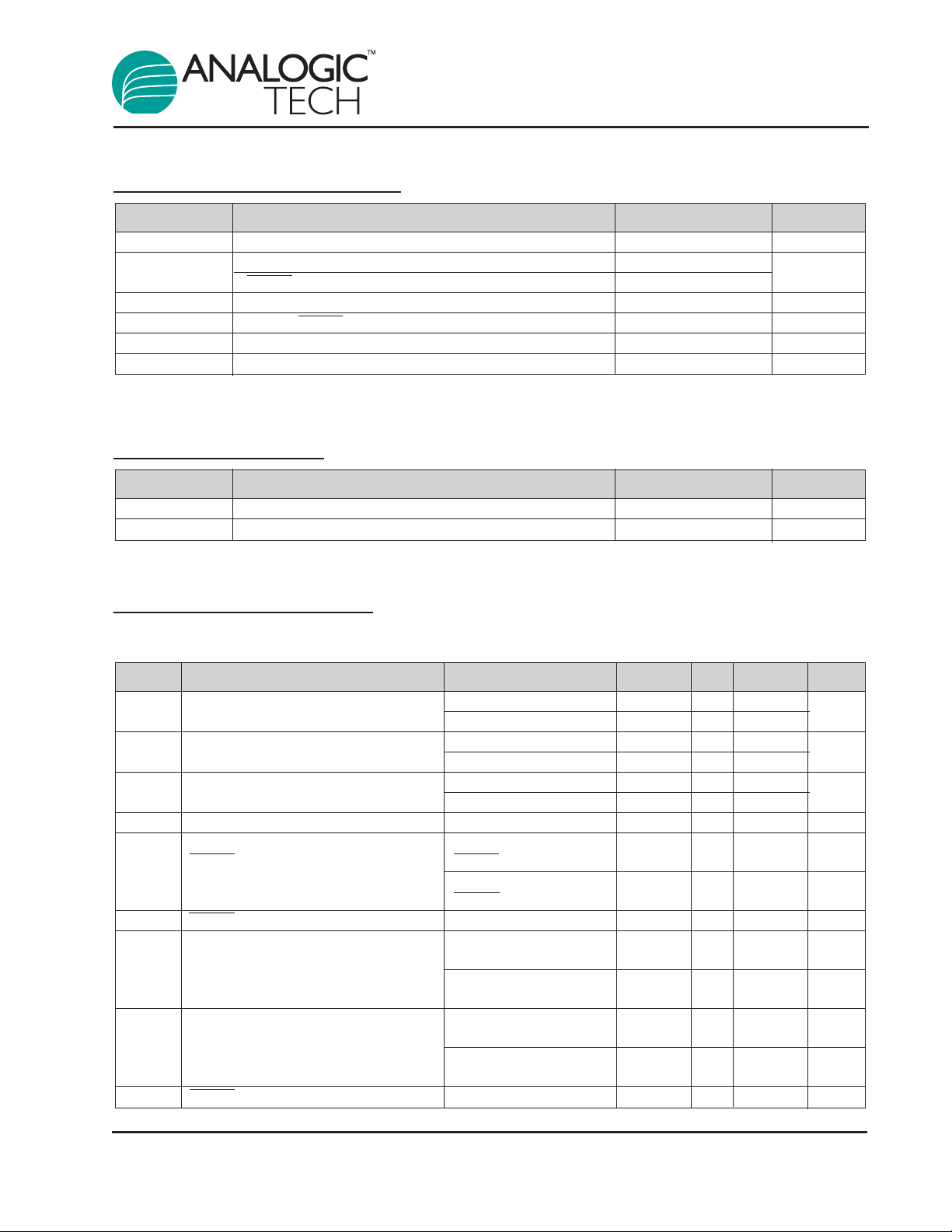
Typical Characteristics (Unless otherwise noted, V
Supply Current vs. Temperature
1.40
1.20
1.00
0.80
0.60
0.40
Supply Current (µA)
0.20
0.00
-40 -20 0 20 40 60 80
Power-Down Reset Propagation
30
25
20
15
10
5
0
Reset Propagation Delay (µs)
-40 -20 0 20 40 60 80
VCC=5V
VCC=3V
Temperature (°C)
Delay vs. Temperature
VOD=10mV
VOD=100mV
Maximum Transient
Temperature (°C)
= 5V, TA= 25°C)
IN
Normalized Reset Threshold
vs. Temperature
1.003
1.002
1.001
1.000
0.999
0.998
Normalized Threshold
0.997
-40 -20 0 20 40 60 80
Temperature (°C)
Maximum Transient Duration
vs. Reset Threshold Overdrive
400
350
300
250
200
150
100
Duration (µS)
50
0
1 10 100 1000
Reset Threshold Overdrive,
VTH-V
(mV)
CC
4 3560.2002.3.0.91
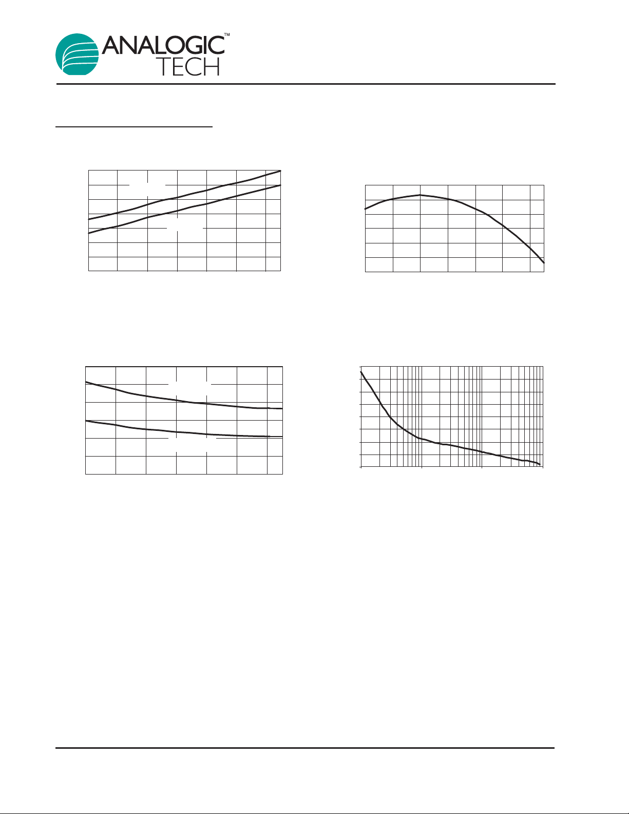
Functional Block Diagram
V
CC
+
-
GND
AAT3560/2/4
NanoPower Voltage Detector
+
RESET (RESET)
-
V
REF
Functional Description
General
The AAT3560 series of Nanopower voltage detectors, monitors a system power supply and asserts
an output signal (Low for AAT3562, AAT3564 and
High for AAT3560) when the supply voltage drops
V
IN
Minimum Operating
Voltage
Output
Voltage
Ground
Ground
below a factory programmed threshold voltage.
The output signal will remain valid until the input
voltage falls below the Minimum Operating Voltage
of 1V. Below this value the output voltage is undefined. When the input voltage rises above the factory programmed threshold, the output signal will
resume its inactive state.
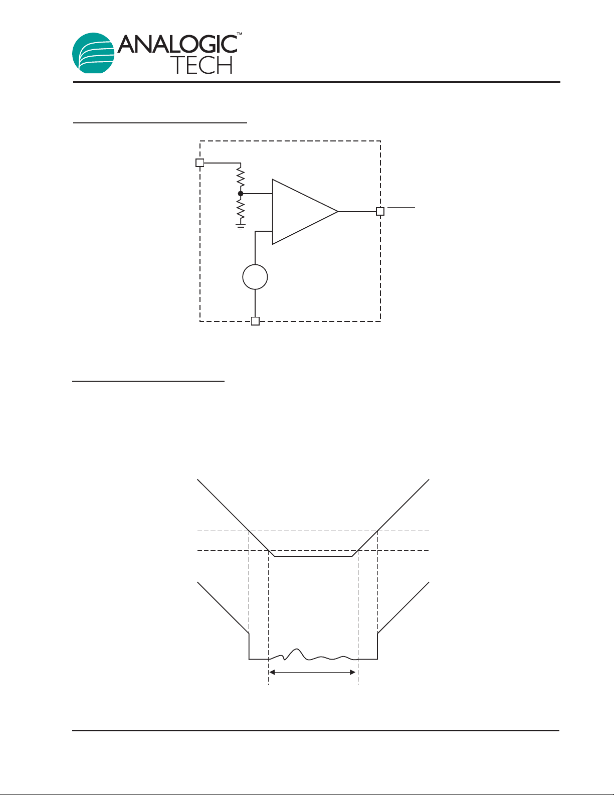
Detection Voltage
Level
Output Voltage
Undefined
Figure 1. AAT3562 Timing Diagram
3560.2002.3.0.91 5

AAT3560/2/4
NanoPower Voltage Detector
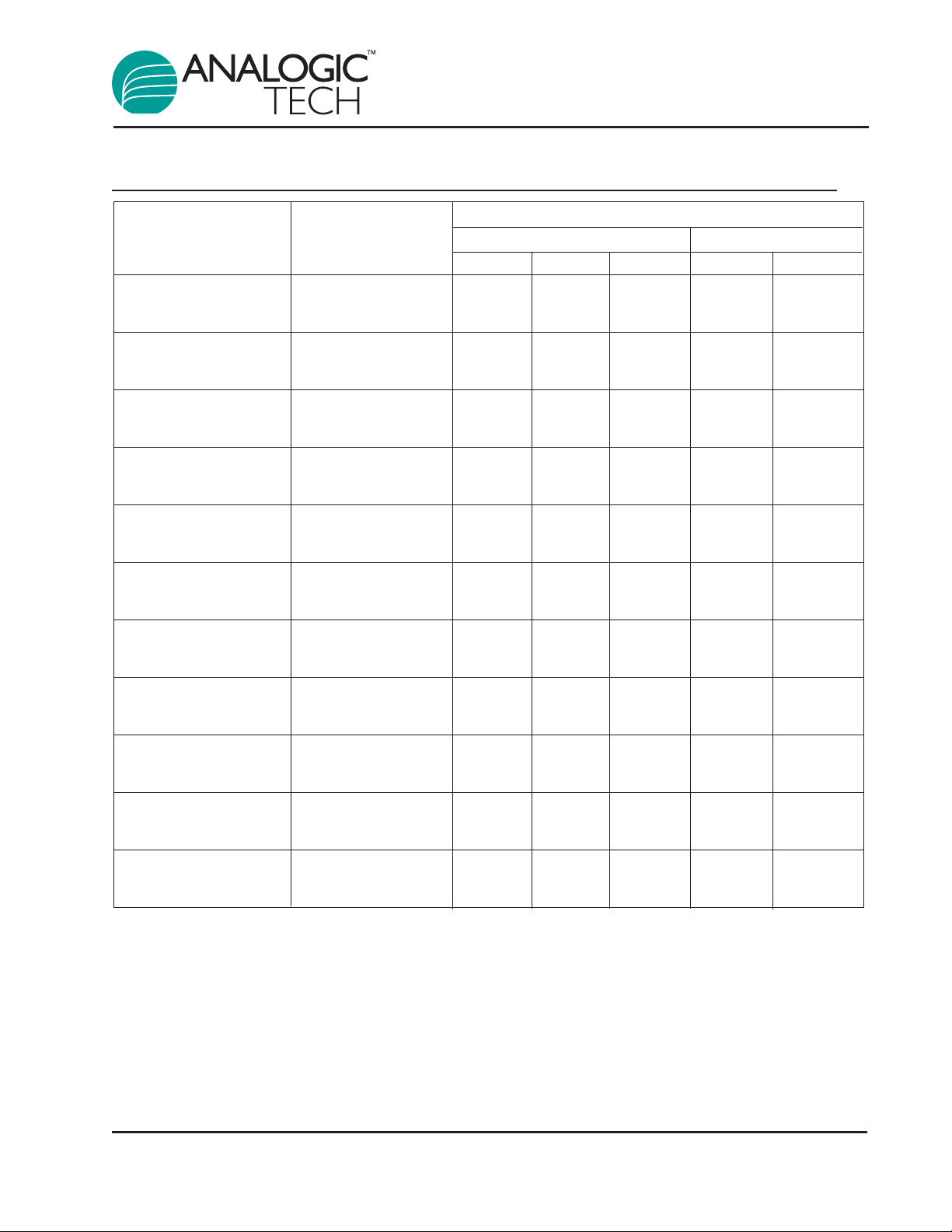
Factory Trimmed Reset Thresholds* and Ordering Information Table 1
Reset Threshold Voltage, VTH(V)
T
Ordering Package
Part Number Marking Code MIN TYP MAX MIN MAX
AAT3560IGY-2.20-T1
AAT3562IGY-2.20-T1 2.167 2.200 2.233 2.145 2.255
AAT3564IGY-2.20-T1
AAT3560IGY-2.30-T1
AAT3562IGY-2.30-T1 2.266 2.300 2.335 2.243 2.358
AAT3564IGY-2.30-T1
AAT3560IGY-2.40-T1
AAT3562IGY-2.40-T1 2.364 2.400 2.436 2.340 2.460
AAT3564IGY-2.40-T1
AAT3560IGY-2.50-T1
AAT3562IGY-2.50-T1 2.463 2.500 2.538 2.438 2.563
AAT3564IGY-2.50-T1
AAT3560IGY-2.60-T1
AAT3562IGY-2.60-T1 2.561 2.600 2.639 2.535 2.665
AAT3564IGY-2.60-T1
AAT3560IGY-2.70-T1
AAT3562IGY-2.70-T1 2.660 2.700 2.741 2.633 2.768
AAT3564IGY-2.70-T1
AAT3560IGY-2.80-T1
AAT3562IGY-2.80-T1 2.758 2.800 2.842 2.730 2.870
AAT3564IGY-2.80-T1
AAT3560IGY-2.90-T1
AAT3562IGY-2.90-T1 2.857 2.900 2.944 2.828 2.973
AAT3564IGY-2.90-T1
AAT3560IGY-3.00-T1
AAT3562IGY-3.00-T1 2.955 3.000 3.045 2.925 3.075
AAT3564IGY-3.00-T1
AAT3560IGY-3.10-T1
AAT3562IGY-3.10-T1 3.054 3.100 3.147 3.023 3.178
AAT3564IGY-3.10-T1
AAT3560IGY-3.20-T1
AAT3562IGY-3.20-T1 3.152 3.200 3.248 3.120 3.280
AAT3564IGY-3.20-T1
AAT3560IGY-3.30-T1
AAT3562IGY-3.30-T1 3.251 3.300 3.350 3.218 3.383
AAT3564IGY-3.30-T1
AAT3560IGY-3.40-T1
AAT3562IGY-3.40-T1 3.349 3.400 3.451 3.315 3.485
AAT3564IGY-3.40-T1
AAT3560IGY-3.50-T1
AAT3562IGY-3.50-T1 3.448 3.500 3.553 3.413 3.588
AAT3564IGY-3.50-T1
= 25ºC TA= -40 to +85ºC
A
6 3560.2002.3.0.91
AAT3560/2/4
NanoPower Voltage Detector
Factory Trimmed Reset Thresholds* and Ordering Information Table 1
Reset Threshold Voltage, VTH(V)
T
Ordering Package
Part Number Marking Code MIN TYP MAX MIN MAX
AAT3560IGY-3.60-T1
AAT3562IGY-3.60-T1 3.546 3.600 3.654 3.510 3.690
AAT3564IGY-3.60-T1
AAT3560IGY-3.70-T1
AAT3562IGY-3.70-T1 3.644 3.700 3.755 3.607 3.792
AAT3564IGY-3.70-T1
AAT3560IGY-3.80-T1
AAT3562IGY-3.80-T1 3.743 3.800 3.857 3.705 3.895
AAT3564IGY-3.80-T1
AAT3560IGY-3.90-T1
AAT3562IGY-3.90-T1 3.841 3.900 3.958 3.802 3.997
AAT3564IGY-3.90-T1
AAT3560IGY-4.00-T1
AAT3562IGY-4.00-T1 3.940 4.000 4.060 3.900 4.100
AAT3564IGY-4.00-T1
AAT3560IGY-4.10-T1
AAT3562IGY-4.10-T1 4.038 4.100 4.161 3.997 4.202
AAT3564IGY-4.10-T1
AAT3560IGY-4.20-T1
AAT3562IGY-4.20-T1 4.137 4.200 4.263 4.095 4.305
AAT3564IGY-4.20-T1
AAT3560IGY-4.30-T1
AAT3562IGY-4.30-T1 4.235 4.300 4.364 4.192 4.407
AAT3564IGY-4.30-T1
AAT3560IGY-4.40-T1
AAT3562IGY-4.40-T1 4.334 4.400 4.466 4.290 4.510
AAT3564IGY-4.40-T1
AAT3560IGY-4.50-T1
AAT3562IGY-4.50-T1 4.432 4.500 4.567 4.387 4.612
AAT3564IGY-4.50-T1
AAT3560IGY-4.60-T1
AAT3562IGY-4.60-T1 4.531 4.600 4.669 4.485 4.715
AAT3564IGY-4.60-T1
Contact Local Sales Office for custom trimmed options.
= 25ºC TA= -40 to +85ºC
A
3560.2002.3.0.91 7

Package Information
SOT23-3
AAT3560/2/4
NanoPower Voltage Detector
A2
D
S1
Dim
Millimeters Inches
Min Max Min Max
A .887 1.02 0.034 .040
A1 .013 0.10 0.0005 .004
A2 - - - -
E
H
b 0.37 0.51 0.015 0.020
C 0.085 0.180 0.003 0.007
D 2.80 3.04 0.110 0.120
E 1.20 1.40 0.047 0.055
S
e
e 1.78 2.05 0.070 0.080
H 2.10 2.64 0.083 0.104
L - 0.69 - 0.027
S 0.45 0.60 0.018 0.024
S1 0.89 1.03 0.035 0.040
θ1 0° 8° 0° 8°
A
1
A1
b
Θ
L
Note:
1. PACKAGE BODY SIZE EXCLUDE MOLD FLASH
PROTRUSIONS OR GATE BURRS.
C
2. TOLERANCE ±0.1000 mm (4mi) UNLESS OTHERWISE SPECIFIED
3. COPLANARITY: 0.1000
4. DIMENSION L IS MEASURED IN GAGE PLANE
Advanced Analogic Technologies, Inc.
1250 Oakmead Parkway, Suite 310, Sunnyvale, CA 94086
Phone (408) 524-9684
Fax (408) 524-9689
8 3560.2002.3.0.91
 Loading...