

AAT3152
High Efficiency 1X/1.5X/2X Charge Pump
For White LED Applications
3152.2005.08.1.2 1
ChargePump
™
General Description
The AAT3152 is a low noise, constant frequency
charge pump DC/DC converter that uses a tri-mode
load switch (1X), fractional (1.5X), and doubling (2X)
conversion to maximize efficiency for white LED
applications. The AAT3152 is capable of driving
four-channel LEDs from a 2.7V to 5.5V input. The
current sinks may be operated individually or in parallel for driving higher-current LEDs. A low external
parts count (two 1µF flying capacitors and two small
1µF capacitors at VINand V
OUT
) makes this part ide-
ally suited for small, battery-powered applications.
AnalogicTech's S2Cwire™ (Simple Serial Control™)
serial digital input is used to enable, disable, and
set current for each LED with eight settings (20mA
down to 50µA) including main/sub-display group
control. The AAT3152 consumes extremely low current internally (50µA typical) at light load for optimized efficiency.
Each output of the AAT3152 is equipped with builtin protection for V
OUT
short-circuit and auto-disable
for load short-circuit conditions. Built-in soft-start
circuitry prevents excessive inrush current during
start-up. A low current shutdown feature disconnects the load from VINand reduces quiescent current to less than 1µA.
The AAT3152 is available in a Pb-free, space-saving, thermally-enhanced 12-pin 3x3mm TDFN
package.
Features
•VINRange: 2.7V to 5.5V
• Fully Programmable Current with Single Wire
— Eight-Step Current: 20mAto 50µA
— Individual Main-Sub Group Control
— Low IQ(50µA) at Light Load
• Tri-Mode 1X, 1.5X, and 2X Charge Pump for
Maximum Efficiency and VFCoverage
• Drives 1-4 Channels of LEDs
• No Inductors, Low Noise Operation
• 1MHz Constant Switching Frequency
• Small Application Circuit
• Built-In Thermal Protection
• Built-In Auto-Disable for Short-Circuit
• Automatic Soft Start
•IQ<1µA in Shutdown
• Thermally-Enhanced 3x3mm 12-Pin TDFN
Package
Applications
• Color (RGB) Lighting
• Programmable Current Sinks
• White LED Backlighting
• White Photo Flash for Digital Still Cameras
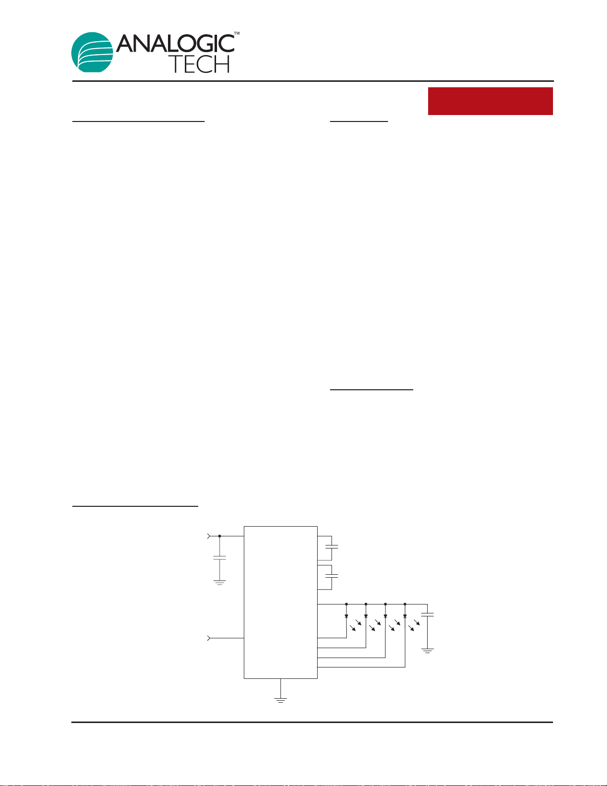
Typical Application
T
C
1µF
VIN
IN
AAT3152
EN/SET
GND
C1+
C1C2+
C2-
VOUT
D1
D2
D3
D4
C1
1µF
C2
1µF
D1 D2 D3 D4
C
1µF
OU
2.7V to 5.5V
EN/SET

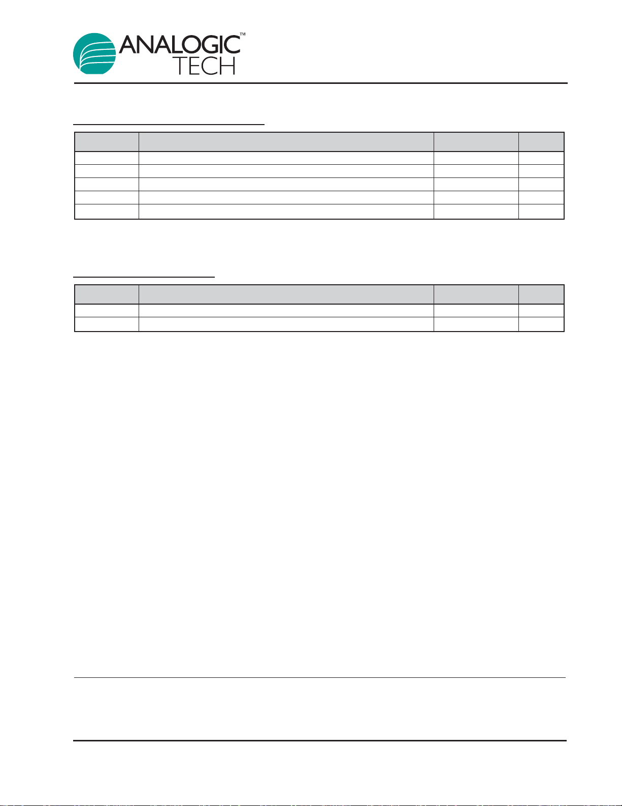
Pin Descriptions
Pin Configuration
TDFN33-12
(TopView)
Pin # Symbol Function
1 D4 Current sink input #4.
2 EN/SET S2Cwire serial interface control pin.
3 C1+ Flying capacitor 1 positive terminal. Connect a 1µF capacitor between C1+
and C1-.
4 C1- Flying capacitor 1 negative terminal.
5 VOUT Charge pump output to drive load circuit. Requires 1µF capacitor connected
between this pin and ground.
6 C2+ Flying capacitor 2 positive terminal. Connect a 1µF capacitor between C2+
and C2-.
7 C2- Flying capacitor 2 negative terminal.
8 VIN Input power supply. Requires 1µF capacitor connected between this pin and
ground.
9 GND Ground.
10 D1 Current sink input #1.
11 D2 Current sink input #2.
12 D3 Current sink input #3.
EP Exposed paddle (bottom); connect to GND directly beneath package.
AAT3152
High Efficiency 1X/1.5X/2X Charge Pump
For White LED Applications
2 3152.2005.08.1.2
D4
EN/SET
C1+
C1-
VOUT
C2+
1
2
3
4
5
6
12
11
10
9
8
7
D3
D2
D1
GND
VIN
C2-
Absolute Maximum Ratings
1
Thermal Information
3
Symbol Description Value Units
P
D
Maximum Power Dissipation
4
2.0 W
θ
JA
Maximum Thermal Resistance 50 °C/W
Symbol Description Value Units
V
IN
Input Voltage -0.3 to 6 V
V
EN/SET
EN/SET to GND Voltage -0.3 to VIN+ 0.3 V
I
OUT
2
Maximum DC Output Current 150 mA
T
J
Operating Junction Temperature Range -40 to 150 °C
T
LEAD
Maximum Soldering Temperature (at leads, 10 sec) 300 °C
AAT3152
High Efficiency 1X/1.5X/2X Charge Pump
For White LED Applications
3152.2005.08.1.2 3
1. Stresses above those listed in Absolute Maximum Ratings may cause permanent damage to the device. Functional operation at conditions other than the operating conditions specified is not implied. Only one Absolute Maximum Rating should be applied at any one time.
2. Based on long-term current density limitation.
3. Mounted on an FR4 board.
4. Derate 20mW/°C above 25°C.

Electrical Characteristics
1
CIN= C
OUT
= C1= C2= 1.0µF; TA= -40°C to +85°C, unless otherwise noted.
Typical values are TA= 25°C, VIN= 3.6V.
Symbol Description Conditions Min Typ Max Units
Input Power Supply
V
IN
Operation Range 2.7 5.5 V
1X Mode, 3.0 ≤ V
IN
≤ 5.5, Active, 0.3 1
No Load Current
1.5X Mode, 3.0 ≤ V
IN
≤ 5.5, Active, 1 3 mA
I
CC
Operating Current No Load Current
2X Mode, 3.0 ≤ V
IN
≤ 5.5, Active, 1.5 3
No Load Current
50µA Setting, 1X Mode 50 µA
I
SHDN
Shutdown Current EN/SET = 0 1 µA
I
DX
I
SINK
Average Current Accuracy I
SET
= 20mA, TA= 25°C -10 10 %
I
(D-Match)
Current Matching Between Any VF:D1:D4 = 3.6V 0.5 %
Two Current Sink Inputs
2, 3
V
TH
1X to 1.5X or 1.5X to 2X Transition 150 mV
Threshold at Any Current Sink Pin
Charge Pump Section
T
SS
Soft-Start Time 100 µs
F
CLK
Clock Frequency 1000 kHz
EN/SET
V
EN(L)
Enable Threshold Low 0.4 V
V
EN(H)
Enable Threshold High 1.4 V
T
EN/SET LO
EN/SET Low Time 0.3 75 µs
T
EN/SET_HI_MIN
Minimum EN/SET High Time 50 ns
T
EN/SET_HI_MAX
Maximum EN/SET High Time 75 µs
T
OFF
EN/SET Off Timeout 500 µs
T
LAT
EN/SET Latch Timeout 500 µs
I
EN/SET
EN/SET Input Leakage -1 1 µA
AAT3152
High Efficiency 1X/1.5X/2X Charge Pump
For White LED Applications
4 3152.2005.08.1.2
1. The AAT3152 is guaranteed to meet performance specifications over the -40°C to +85°C operating temperature range and is assured
by design, characterization, and correlation with statistical process controls.
2. Current matching is defined as the deviation of any sink current at I
OUT
= 20mA and 2mA.
3. Specification applies only to the tri-mode charge pump.

Typical Characteristics
µ
µ
µ
µ
AAT3152
High Efficiency 1X/1.5X/2X Charge Pump
For White LED Applications
3152.2005.08.1.2 5
Efficiency vs. Supply Voltage
100
90
80
70
Efficiency (%)
60
50
2.8 3.0 3.2 3.4 3.6 3.8 4.0 4 .2
V
10mA
F
= 3.1V
Supply Voltage (V)
V
20mA
F
= 3.4V
Turn-On to 1.5X Mode
(VIN = 3.5V; 20mA Load)
EN
(2V/div)
CP
(2V/div)
V
(500mV/div)
(200mA/div)
SINK
I
IN
EN
(2V/div)
CP
(2V/div)
V
SINK
(500mV/div)
(200mA/div)
EN
(2V/div)
CP
(2V/div)
V
SINK
(500mV/div)
(200mA/div)
Turn-On to 1X Mode
(VIN = 4.2V; 20mA Load)
I
IN
100µ
s/div
Turn-On to 2X Mode
(VIN = 2.8V; 20mA Load)
I
IN
100µ
s/div
Turn-Off from 1.5X Mode
Current Matching vs. Temperature
100µ
s/div
(VIN = 3.5V; 20mA Load)
20.4
EN
(2V/div)
V
(1V/div)
(100mA/div)
F
I
IN
500µ
s/div
Channel 2
20.2
20.0
Channel 4
19.8
19.6
19.4
Current (mA)
19.2
19.0
-40 -20 0 20 40 60 80
Channel 3 Channel 1
Temperature (°°C)

Typical Characteristics
µ
µ
AAT3152
High Efficiency 1X/1.5X/2X Charge Pump
For White LED Applications
6 3152.2005.08.1.2
(40mV/div)
V
CP
(40mV/div)
V
SINK
(40mV/div)
V
(40mV/div)
CP
(40mV/div)
Load Characteristics
(VIN = 3.7V; 1.5X Mode; 14mA Load)
IN
500ns/div
Load Characteristics
(VIN = 3.9V; 1.5X Mode; 20mA Load)
IN
(40mV/div)
V
CP
(40mV/div)
V
SINK
(40mV/div)
V
(40mV/div)
CP
(40mV/div)
Load Characteristics
(VIN = 2.7V; 2X Mode; 14mA Load)
IN
500ns/div
Load Characteristics
(VIN = 2.9V; 2X Mode; 20mA Load)
IN
V
SINK
(40mV/div)
500ns/div
T
vs. V
LAT
350
300
250
s)
200
(µ
150
LAT
T
100
50
0
2.7 2.9 3.1 3.3 3.5 3.7 3.9 4.1 4.3 4.5 4.7 4.9 5.1 5.3 5.5
-40°C
25°C 85°C
IN
VIN (V)
V
SINK
(40mV/div)
500ns/div
T
vs. V
OFF
400
350
300
250
s)
200
(µ
OFF
150
T
100
50
0
2.7 2.9 3.1 3.3 3.5 3.7 3.9 4.1 4.3 4.5 4.7 4.9 5.1 5.3 5.5
-40°C
IN
25°C 85°C
VIN (V)

Typical Characteristics
AAT3152
High Efficiency 1X/1.5X/2X Charge Pump
For White LED Applications
3152.2005.08.1.2 7
Input Ripple vs. Input Voltage
18
16
14
12
10
8
6
Amplitude (mV)
4
2
0
2.5 2.67 2.84 3.01 3.18 3.35 3.52 3.69 3.86 4.03 4.2
10mA
Input Voltage (V)
1.2
1.1
1
-40°C
2.7 2.9 3.1 3.3 3.5 3.7 3.9 4.1 4.3 4.5 4.7 4.9 5.1 5.3 5.5
(V)
IH
V
0.9
0.8
0.7
0.6
0.5
0.4
0.3
0.2
20mA
VIL vs. V
IN
25°C 85°C
V
(V)
IN
VIH vs. V
1.2
1.1
1
-40°C
2.7 2.9 3.1 3.3 3.5 3.7 3.9 4.1 4.3 4.5 4.7 4.9 5.1 5.3 5.5
(V)
IH
V
0.9
0.8
0.7
0.6
0.5
0.4
0.3
0.2
IN
25°C 85°C
VIN (V)

AAT3152
High Efficiency 1X/1.5X/2X Charge Pump
For White LED Applications
8 3152.2005.08.1.2
Functional Block Diagram
Functional Description
The AAT3152 is a tri-mode load switch (1X) and
high efficiency (1.5X or 2X) charge pump device
intended for white LED backlight applications. To
maximize power conversion efficiency, an internal
sensing circuit monitors the voltage required on
each constant current sink input and sets the load
switch and charge pump modes based on the input
battery voltage and the current sink input voltage.
As the battery discharges over time, the AAT3152
charge pump is enabled when any of the four current sink inputs near dropout. The charge pump initially starts in 1.5X mode. If the charge pump output drops enough for any current source output to
become close to dropout, the charge pump will
automatically transition to 2X mode. The AAT3152
requires only four external components: two 1µF
ceramic capacitors for the charge pump flying
capacitors (C
1
and C2), one 1µF ceramic input
capacitor (CIN), and one 0.33µF to 1µF ceramic
charge pump output capacitor (C
OUT
).
The four constant current sink inputs (D1 to D4)
can drive four individual LEDs with a maximum current of 20mAeach. The unused sink inputs must be
connected to V
OUT
, otherwise the part will operate
only in 2X charge pump mode. The S2Cwire serial
interface enables the AAT3152 and sets the current sink magnitudes. S2Cwire addressing allows
independent control of two groups of current sink
input: D1-D3 and D4.
C1+ C1- C2+ C2-
VIN
Soft-Start
Control
1MHz
Oscillator
Voltage
Reference
EN/SET
S2Cwire
Interface
1X, 1.5X and 2X
Charge Pump
6 x 16 bit
ROM
6 x 16 bit
ROM
D/A
D/A
D/A
D/A
VOUT
D1
D2
D3
D4
GND

Constant Current Output Level Settings
The constant current sink levels for D1 to D4 are
set via the serial interface. No PWM (pulse width
modulation) or additional control circuitry is needed
to control LED brightness. This feature greatly
reduces the burden on a microcontroller or system
IC to manage LED or display brightness, allowing
the user to "set it and forget it." With its high-speed
serial interface (up to 1MHz data rate), the input
sink current of the AAT3152 can be changed successively to brighten or dim LEDs, giving the users
real-time control of LED brightness. Because the
inputs D1 to D4 are true independent constant current sinks, the voltage observed on any single
given input will be determined by the actual forward
voltage (V
F
) for the LED being driven.
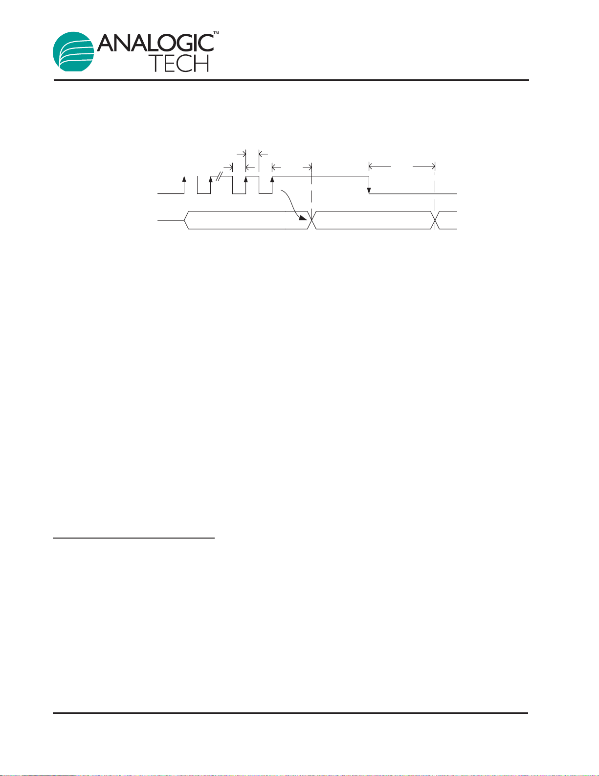
S2Cwire Serial Interface
The current sink input magnitude on the AAT3152 is
controlled by AnalogicTech's S2Cwire serial digital
input. It relies on the number of rising edges of the
EN/SET pin to address and load the registers.
S2Cwire latches data or address after the EN/SET
pin has been held high for time T
LAT
. The interface
records rising edges of the EN/SET pin and
decodes them into 16 different states, as indicated
in the Current Setting table. There are four brightness levels for main or sub-display group with the
possibility of individually turning ON or OFF each
group. To further optimize power efficiency, the
AAT3152 also offers four low-current levels for dim
LED operation (Data 13-16). During this low-current
mode, the internal supply current reduces to only
80µA typical.
The counter can be clocked at speeds up to 1MHz,
such that intermediate states are not visible. The
first rising edge of EN/SET enables the IC and initially sets the output LED current to 20mA. Once
the final clock cycle is input for the desired brightness level, the EN/SET pin is held high to maintain
the device output current at the programmed level.
The device is disabled 500µs (T
OFF
) after the
EN/SET pin transitions to a logic low state.
AAT3152 Current Setting
The EN/SET timing is designed to accommodate a
wide range of data rates. After the first rising edge
of EN/SET, the charge pump is enabled and reaches full capacity after the soft-start time (TSS). During
the soft-start time, multiple clock pulses may be
entered on the EN/SET pin to set the final output
current level with a single burst of clocks.
Alternatively, the EN/SET clock pulses may be
entered one at a time to gradually increase the
LED brightness over any desired time period. The
current outputs remain constant as long as
EN/SET remains in a logic high state. The current
outputs are switched off after EN/SET has
remained in a low state for at least the T
OFF
timeout
period; then, the AAT3152 enters shutdown mode
and draws less than 1µA from VIN. Data are reset
to 0 during shutdown.
Main Group Sub Group
(D1-D3) (D4)
Data I
OUT
(mA) I
OUT
(mA)
120 20
214 14
310 10
47 7
520 0
614 0
710 0
87 0
90 20
10 0 14
11 0 10
12 0 7
13 0.05 0.05
14 0.5 0.5
15 1 1
16 2 2
AAT3152
High Efficiency 1X/1.5X/2X Charge Pump
For White LED Applications
3152.2005.08.1.2 9
AAT3152
High Efficiency 1X/1.5X/2X Charge Pump
For White LED Applications
10 3152.2005.08.1.2
Auto-Disable Feature
The AAT3152 is equipped with an auto-disable feature for each LED channel. After the IC is enabled
and started up, a test current of 150µA (typical) is
forced through each sink channel. The channel will
be disabled if the voltage of that particular current
sink pin does not drop to a certain threshold. This
feature is very convenient for disabling an unused
channel (by tying the DX pin to V
OUT
) or during an
LED fail short event.
Thermal Protection
The AAT3152 has a built-in thermal protection circuit that will shut down the charge pump if the die
temperature rises above the thermal limit, as is the
case during a short circuit of the V
OUT
pin.
Applications Information
LED Selection
Although the AAT3152 is specifically intended for
driving white LEDs, the device can also be used to
drive most types of LEDs with forward voltage
specifications ranging from 2.0V to 4.7V. LED
applications may include main and sub-LCD display backlighting, camera photo-flash applications,
color (RGB) LEDs, infrared (IR) diodes for remotes,
and other loads benefiting from a controlled output
current generated from a varying input voltage.
Since the D1 to D4 input current sinks are matched
with negligible voltage dependence, the LED
brightness will be matched regardless of the specific LED forward voltage (VF) levels. In some
instances (e.g., in high-luminous-output applications such as photo-flash), it may be necessary to
drive high-VFtype LEDs. The low-dropout current
sinks in the AAT3152 make it capable of driving
LEDs with forward voltages as high as 4.7V at full
current from an input supply as low as 3.0V.
Outputs can be paralleled to drive high-current
LEDs without complication.
Device Switching Noise Performance
The AAT3152 operates at a fixed frequency of
approximately 1MHz to control noise and limit harmonics that can interfere with the RF operation of
cellular telephone handsets or other communication devices. Back-injected noise appearing on the
input pin of the charge pump is 20mV peak-topeak, typically ten times less than inductor-based
DC/DC boost converter white LED backlight solutions. The AAT3152 soft-start feature prevents
noise transient effects associated with in-rush currents during start-up of the charge pump circuit.
Capacitor Selection
Careful selection of the four external capacitors
CIN, C1, C2, and C
OUT
is important because they will
affect turn-on time, output ripple, and transient per-
S2Cwire Serial Interface Timing
EN/SET
1
2 n n <= 16
T
HI
T
LO
T
LAT
T
OFF
Data Reg
1n
0

AAT3152
High Efficiency 1X/1.5X/2X Charge Pump
For White LED Applications
3152.2005.08.1.2 11
formance. Optimum performance will be obtained
when low Equivalent Series Resistance (ESR)
ceramic capacitors are used. In general, low ESR
may be defined as less than 100mΩ. A value of
1µF for all four capacitors is a good starting point
when choosing capacitors. If the LED current
sources are only programmed for light current levels, then the capacitor size may be decreased.
Capacitor Characteristics
Ceramic composition capacitors are highly recommended over all other types of capacitors for use
with the AAT3152. Ceramic capacitors offer many
advantages over their tantalum and aluminum electrolytic counterparts. A ceramic capacitor typically
has very low ESR, is lowest cost, has a smaller
PCB footprint, and is non-polarized. Low ESR
ceramic capacitors help to maximize charge pump
transient response. Since ceramic capacitors are
non-polarized, they are not prone to incorrect connection damage.
Equivalent Series Resistance
ESR is an important characteristic to consider when
selecting a capacitor . ESR is a resistance internal to
a capacitor that is caused by the leads, internal
connections, size or area, material composition,
and ambient temperature. Capacitor ESR is typical-
ly measured in milliohms for ceramic capacitors and
can range to more than several ohms for tantalum
or aluminum electrolytic capacitors.
Ceramic Capacitor Materials
Ceramic capacitors less than 0.1µF are typically
made from NPO or C0G materials. NPO and C0G
materials typically have tight tolerance and are stable over temperature. Larger capacitor values are
typically composed of X7R, X5R, Z5U, or Y5V
dielectric materials. Large ceramic capacitors, typically greater than 2.2µF, are often available in lowcost Y5V and Z5U dielectrics, but capacitors
greater than 1µF are typically not required for
AAT3152 applications. Capacitor area is another
contributor to ESR. Capacitors that are physically
large will have a lower ESR when compared to an
equivalent material, smaller capacitor . These larger
devices can improve circuit transient response
when compared to an equal value capacitor in a
smaller package size.
Thermal Protection
The AAT3152 has a built-in thermal protection circuit that will shut down the charge pump if the die
temperature rises above the thermal limit, as is the
case during a short circuit of the V
OUT
pin.
AAT3152
High Efficiency 1X/1.5X/2X Charge Pump
For White LED Applications
12 3152.2005.08.1.2
Advanced Analogic Technologies, Inc.
830 E. Arques Avenue, Sunnyvale, CA 94085
Phone (408) 737-4600
Fax (408) 737-4611
AnalogicTech cannot assume responsibility for use of any circuitry other than circuitry entirely embodied in an AnalogicTech product. No circuit patent licenses, copyrights, mask work
rights, or other intellectual property rights are implied.
AnalogicTech reserves the right to make changes to their products or specifications or to discontinue any product or service without notice, and advise customers to obtain the latest
version of relevant information to verify, before placing orders, that information being relied on is current and complete. All products are sold subject to the terms and conditions of sale
supplied at the time of order acknowledgement, including those pertaining to warranty, patent infringement, and limitation of l iability.
AnalogicTech warrants performance of its semiconductor products to the specifications applicable at the time of sale in accordance with AnalogicTech’s standard warranty. Testing and
other quality control techniques are utilized to the extent AnalogicTech deems necessary to support this warranty. Specific testing of all parameters of each device is not necessarily
performed.
Ordering Information
Package Information
All dimensions in millimeters.
Package Marking
1
Part Number (Tape and Reel)
2
TDFN33-12 NQXYY AAT3152IWP-T1
1. XYY = assembly and date code.
2. Sample stock is generally held on part numbers listed in BOLD.
All AnalogicTech products are offered in Pb-free packaging. The term “Pb-free” means
semiconductor products that are in compliance with current RoHS standards, including
the requirement that lead not exceed 0.1% by weight in homogeneous materials. For more
information, please visit our website at http://www.analogictech.com/pbfree.
Detail "A"
3.00 ± 0.05
Top View
Index Area
(D/2 x E/2)
3.00 ± 0.05
Detail "B"
1.70 ± 0.05
Bottom View
0.16
0.375 ± 0.125
2.40 ± 0.05
0.3 ± 0.10
Pin 1 Indicator
(optional)
0.075 ± 0.075
0.1 REF
0.45 ± 0.050.23 ± 0.05
7.5° ± 7.5°
+ 0.05
0.8
-0.20
0.05 ± 0.05
Side View
0.229 ± 0.051
Option A:
C0.30 (4x) max
Chamfered corner
Option B:
R0.30 (4x) max
Round corner
Detail "A"
Detail "B"
 Loading...