


AAT3112
500mA High Efficiency Charge Pump
for White LED Flash Applications
Typical Application
3112.2004.12.1.2 1
ChargePump
™
General Description
The AAT3112 is a member of AnalogicTech's Total
Power Management IC™ (TPMIC™) family. It is a
dual voltage doubling charge pump that provides a
regulated output voltage. It operates with an input
voltage range of 2.7 to 5.0 volts. The device can
deliver a constant 200mAoutput load current and up
to 500mA of pulsed current. The 500mA peak current capability of the AAT3112 makes it ideal for
white LED flash applications. A low external parts
count (two 1µF flying capacitors and two small
capacitors at VINand V
OUT
) makes the AAT31 12 ide-
ally suited for small battery-powered applications.
The AAT3112 has a thermal management system
to protect the device in the event of a short-circuit
condition at the output pin. Built-in soft-start circuitry prevents excessive inrush current during startup. A high charge pump switching frequency
enables the use of very small external capacitors.
A low current shutdown feature disconnects the
load from VINand reduces quiescent current to less
than 1µA. The AAT3112 is available in a 16-pin
3x3mm QFN package and is rated over the -40°C
to +85°C temperature range.
Features
• Input Voltage Range:
• AAT3112-5.0: 2.7V to 5.0V
• AAT3112-4.5: 2.7V to 4.5V
• Up to 500mA Peak Output Current
• 200mA Continuous Output Current
•IQ<1µA in Shutdown
• Regulated 4.5V or 5.0V Output
• 26µA of Quiescent Current
• Small Application Circuit
• Automatic Soft Start
• No Inductors
• Short-Circuit/Over-Temperature Protection
• 16-Pin 3x3mm QFN Package
• Temperature Range: -40°C to +85°C
Applications
• General-Purpose High-Current Boost Supply
• White LED Backlighting
• White LED Photo Flash
查询AAT3112供应商查询AAT3112供应商
C1 = 1µF C2 = 1µF
C1+C1-C2+C2
V
IN
C
IN
V
IN
AAT3112
Enable Light
Enable Flash
EN1
EN2
GND
-
V
OUT1
C
V
OUT2
D1 D2 D3 D4
OUT
R
B

Pin Descriptions
Pin Configuration
QFN33-16
(Top View)
Pin # Symbol Function
1 N/C No connect.
2 C2+ Flying capacitor 2 positive terminal. Connect 1µF capacitor between C2+ and C2-.
3 C2- Flying capacitor 2 negative terminal.
4 N/C No connect.
5VINInput voltage. Connect to Pin 11.
6 GND Ground connection.
7 EN2 Enable pin. When connected high, Charge Pump 2 is enabled. When connected low, it
disables the charge pump.
8 N/C No connect.
9 EN1 Enable pin. When connected high, Charge Pump 1 is enabled. When connected low, it
disables the charge pump.
10 GND Ground connection.
11 V
IN
Input voltage. Connect to Pin 5.
12 V
OUT1
Output pin for regulated output voltage. Bypass this pin to ground with a low ESR 10µF
capacitor.
13 N/C No connect.
14 C1+ Flying capacitor 1 positive terminal. Connect 1µF capacitor between C1+ and C1-.
15 C1- Flying capacitor 1 negative terminal.
16 V
OUT2
Regulated output voltage 2. Must be connected to V
OUT1
for higher current applications.
If used separately, bypass this pin to ground with a low ESR 10µF capacitor.
EP Exposed paddle (bottom); connect to GND directly beneath package.
AAT3112
500mA High Efficiency Charge Pump
for White LED Flash Applications
2 3112.2004.12.1.2
N/C
C2+
C2-
N/C
V
OUT2
161514
1
2
3
4
567
V
IN
C1+
C1-
GND
EN2
N/C
13
8
N/C
12
11
10
9
V
OUT1
V
IN
GND
EN1

Absolute Maximum Ratings
1
Note 1: Stresses above those listed in Absolute Maximum Ratings may cause permanent damage to the device. Functional operation at conditions other than the operating conditions specified is not implied. Only one Absolute Maximum Rating should be applied at any one time.
Thermal Information
Note 1: Mounted on an FR4 board.
Symbol Description Value Units
P
D
Maximum Power Dissipation 2.0 W
θ
JA
Maximum Thermal Resistance
1
50 °C/W
Symbol Description Value Units
V
IN
Input Voltage -0.3 to 6 V
V
OUT
Charge Pump Output -0.3 to 6 V
V
EN
EN to GND Voltage -0.3 to 6 V
T
J
Operating Junction Temperature Range -40 to 150 °C
T
LEAD
Maximum Soldering Temperature (at leads, 10 sec) 300 °C
AAT3112
500mA High Efficiency Charge Pump
for White LED Flash Applications
3112.2004.12.1.2 3

Electrical Characteristics
VIN= 3.3V, V
OUT
= 5.0V, CIN= C
OUT
= 10 µF, C1 = C2 = 1.0µF; TA= -40°C to 85°C, unless otherwise noted.
Typical values are TA= 25°C.
Notes:
1. The AAT3112 is guaranteed to meet performance specifications over the -40°C to +85°C operating temperature range and is assured
by design, characterization, and correlation with statistical process controls.
2. V
OUT1
and V
OUT2
are pulled high to prevent switching.
Symbol Description Conditions Min Typ Max Units
AAT3112-4.5
Input Power Supply
V
IN
Operation Range 2.7 4.5 V
I
Q
Quiescent Current
2
2.7 ≤ VIN≤ 4.5, I
OUT
= 0 mA; EN1 = EN2 = V
IN
26 60 µA
I
SHDN
Shutdown Current EN1 = EN2 = 0 1.0 µA
I
OUT
Pulsed Output Current
V
IN
= 3.6V; V
OUT
= 4.0V; T
PULSE
= 50mS 590
mA
VIN= 3.6V; V
OUT
=4.0V; T
PULSE
= 500mS 500
V
OUT
Output Voltage
2.7 ≤ V
IN
≤ 4.5, I
OUT
= 100mA 4.32 4.5 4.68
V
3.0 ≤ VIN≤ 4.5, I
OUT
= 200mA 4.32 4.5 4.68
Charge Pump Section
F
CLK
Clock Frequency 750 KHz
η
CP
Charge Pump Efficiency VIN= 2.7V; I
OUT
= 100mA 80 %
EN
V
EN(L)
Enable Threshold Low 0.3 V
V
EN(H)
Enable Threshold High 1.4 V
I
EN
EN Input Leakage -1.0 1.0 µA
AAT3112-5.0
Input Power Supply
V
IN
Operation Range 2.7 5.0 V
I
Q
Quiescent Current
2
2.7 ≤ VIN≤ 5.0, I
OUT
= 0 mA; EN1 = EN2 = V
IN
26 60 µA
I
SHDN
Shutdown Current EN1 = EN2 = 0 1.0 µA
I
OUT
Pulsed Output Current VIN= 3.6V; V
OUT
= 4.5V; T
PULSE
= 50mS 600
mA
VIN= 3.6V; V
OUT
=4.5V; T
PULSE
= 500mS 500
V
OUT
Output Voltage
2.7 ≤ V
IN
≤ 5.0, I
OUT
= 100mA 4.8 5.0 5.2
V
3.0 ≤ VIN≤ 5.0, I
OUT
= 200mA 4.8 5.0 5.2
Charge Pump Section
F
CLK
Clock Frequency 750 KHz
η
CP
Charge Pump Efficiency VIN= 2.7V; I
OUT
= 100mA 85 %
EN
V
EN(L)
Enable Threshold Low 0.3 V
V
EN(H)
Enable Threshold High 1.4 V
I
EN
EN Input Leakage -1.0 1.0 µA
AAT3112
500mA High Efficiency Charge Pump
for White LED Flash Applications
4 3112.2004.12.1.2

AAT3112
500mA High Efficiency Charge Pump
for White LED Flash Applications
3112.2004.12.1.2 5
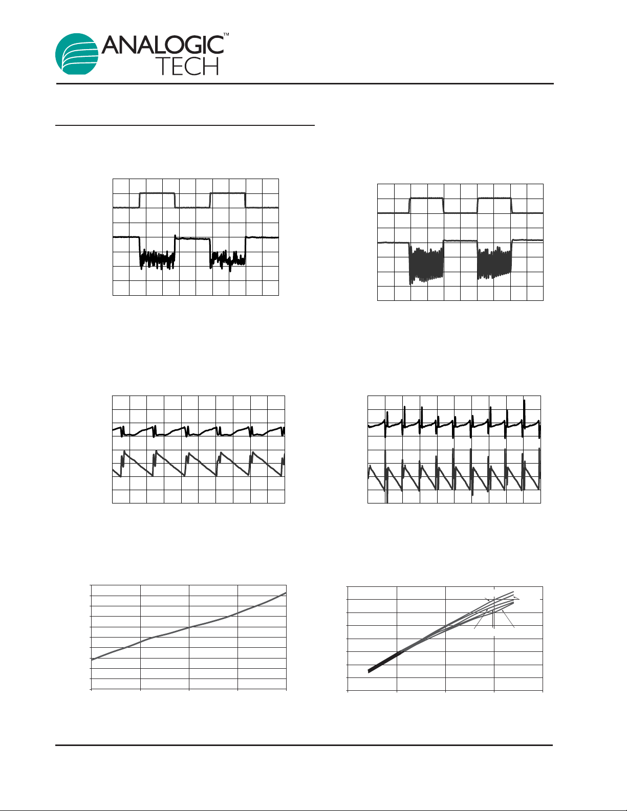
Typical Characteristics
VIN=3.5V, CIN=C
OUT
=10µF, C1=C2=1µF, TA=25°C, unless otherwise noted.
VIN vs. V
1.00
0.95
-40°C
0.90
0.85
0.80
0.75
(V)
IH
0.70
V
0.65
0.60
0.55
0.50
2.0 2.5 3.0 3.5 4.0 4.5 5.0 5.5
25°C
85°C
IH
Input Voltage (V)
V
Threshold vs. Supply Voltage
SHDN
1.00
0.95
0.90
Thre shold (V)
SHDN
V
0.85
0.80
0.75
0.70
0.65
0.60
0.55
0.50
V
IH
V
IL
2.0 2.5 3.0 3.5 4.0 4.5 5.0 5.5
Input Voltage (V)
VIN vs. V
1.00
0.95
0.90
-40°C
25°C
2.0 2.5 3.0 3.5 4.0 4.5 5.0 5.5
(V)
IL
V
0.85
0.80
0.75
0.70
0.65
0.60
0.55
0.50
IL
85°C
Input Voltage (V)

AAT3112
500mA High Efficiency Charge Pump
for White LED Flash Applications
6 3112.2004.12.1.2
Typical Characteristics-AAT3112-4.5V
VIN=3.5V, CIN=C
OUT
=10µF, C1=C2=1µF, TA=25°C, unless otherwise noted.
µ
Output Voltage vs. Output Current
5.0
4.9
4.8
4.7
4.6
4.5
VIN = 4.2V
4.4
4.3
4.2
Output Voltage (V)
4.1
4.0
0 50 100 150 200 250 300
Startup Time with 100mA Load
EN
(2V/div)
V
OUT
(1V/div)
VIN = 3.9VVIN = 3.6V
Output Current (mA)
Supply Current vs. Supply Voltage
(No Load, No Switching)
30
25
A)
20
15
10
5
Supply Current (µ
0
2.5 3.0 3.5 4.0 4.5
Supply Voltage (V)
Startup Time with 200mA Load
EN
(2V/div)
V
OUT
(1V/div)
50µµs/div
Maximum Current Pulse (50ms pulse)
vs. Input Voltage, V
800
700
600
500
400
300
Maximum Current Pulse (mA)
3 3.2 3.4 3.6 3.8 4 4.2
OUT
> 4.0V
85
80
75
70
65
60
55
Efficiency (%)
50
45
40
Efficiency vs. Supply Voltage
50mA
200mA
2.7
2.9 3.1 3.3 3.5 3.7 3.9 4.1 4.3 4.5
Input Voltage (V)
50µµs/div
100mA
Input Voltage (V)

AAT3112
500mA High Efficiency Charge Pump
for White LED Flash Applications
3112.2004.12.1.2 7
Typical Characteristics-AAT3112-4.5V
VIN=3.5V, CIN=C
OUT
=10µF, C1=C2=1µF, TA=25°C, unless otherwise noted.
A
A
I
OUT
(200mA/div)
V
OUT
(20mV/div)
V
IN
C Coupled
(20mV/div)
V
OUT
C Coupled
(20mV/div)
Load Transient Response
(VIN = 3.0V)
50µs/div
Input and Output Ripples
(I
= 50mA @ VIN = 3.5V)
OUT
I
OUT
(200mA/div)
V
OUT
(20mV/div)
AC Coupled
(20mV/div)
V
AC Coupled
(20mV/div)
V
OUT
Load Transient Response
(VIN = 4.2V)
50µs/div
Input and Output Ripples
(I
= 100mA @ VIN = 3.5V)
OUT
IN
5µs/div
Output Current vs. Input Voltage
(500ms Pulse Time; V
800
700
600
500
400
300
200
100
Output Current (mA)
0
2.5 3 3.5 4 4.5
Input Voltage (V)
OUT
> 4.0V)
Output Current vs. Input Voltage (70°C)
800
700
600
500
400
300
200
Output Current (mA)
100
0
2.5 3.0 3.5 4.0 4.5
5µs/div
(V
> 4.0V)
OUT
50ms
200ms 300ms 500ms
Input Voltage (V)
100ms

AAT3112
500mA High Efficiency Charge Pump
for White LED Flash Applications
8 3112.2004.12.1.2
Typical Characteristics-AAT3112-4.5V
VIN=3.5V, CIN=C
OUT
=10µF, C1=C2=1µF, TA=25°C, unless otherwise noted.
Output Voltage vs. Input Voltage for
Pulsed High Current, I
5
4.5
50ms Pulse
4
3.5
3
2.5
2
1.5
1
Output Voltage (V)
0.5
0
343.2 3.4 3.6 3.8 4.2
= 500mA
OUT
500ms Pulse
Input Voltage (V)

AAT3112
500mA High Efficiency Charge Pump
for White LED Flash Applications
3112.2004.12.1.2 9
Typical Characteristics-AAT3112-5.0V
VIN=3.5V, CIN=C
OUT
=10µF, C1=C2=1µF, TA=25°C, unless otherwise noted.
µ
O
(
)
Output Voltage vs. Output Current
5.5
5.4
V
5.3
5.2
5.1
5.0
4.9
4.8
utput Voltage
4.7
4.6
4.5
0 50 100 150 200 250 300
VIN = 4.2V
VIN = 3.6V
Output Current (mA)
Startup Time with 100mA Load
EN
(2V/div)
V
OUT
(1V/div)
VIN = 3.9V
Supply Current vs. Supply Voltage
(No Load, No Switching)
30
25
A)
20
15
10
5
Supply Current (µ
0
2.5 3.0 3.5 4.0 4.5 5.0
Supply Voltage (V)
Startup Time with 200mA Load
EN
(2V/div)
V
OUT
(1V/div)
50µµs/div
Maximum Current Pulse (50ms pulse)
vs. Input Voltage, V
1000
900
800
700
600
500
400
300
Maximum Current Pulse (mA)
3.0 3.2 3.4 3.6 3.8 4.0 4.2
OUT
> 4.5V
95
90
85
80
75
70
65
60
Efficiency (%)
55
50
45
40
Efficiency vs. Supply Voltage
100mA
200mA
50mA
2.7 3.0 3.3 3.5 3.8 4.1 4.4 4.7 4.9
Input Voltage (V)
50µµs/div
Input Voltage (V)
AAT3112
500mA High Efficiency Charge Pump
for White LED Flash Applications
10 3112.2004.12.1.2
Typical Characteristics-AAT3112-5.0V
VIN=3.5V, CIN=C
OUT
=10µF, C1=C2=1µF, TA=25°C, unless otherwise noted.
I
OUT
(200mA/div)
V
OUT
(20mV/div)
AC Coupled
(20mV/div)
V
AC Coupled
(20mV/div)
V
OUT
Load Transient Response
(VIN = 3.0V)
I
OUT
Load Transient Response
(VIN = 4.2V)
(200mA/div)
V
50µs/div
Input and Output Ripples
(I
= 50mA @ VIN = 3.5V)
OUT
IN
OUT
(20mV/div)
V
IN
50µs/div
Input and Output Ripples
(I
= 100mA @ VIN = 3.5V)
OUT
AC Coupled
(20mV/div)
V
OUT
AC Coupled
(20mV/div)
5µs/div
Output Current vs. Input Voltage
(500ms Pulse Time; V
1000
900
800
700
600
500
400
300
200
Output Current (mA)
100
0
3.0 3.5 4.0 4.5 5.0
Input Voltage (V)
OUT
> 4.5V)
Output Current vs. Input Voltage (70°C)
800
700
600
500
400
300
200
Output Current (mA)
100
0
2.5 3.0 3.5 4.0 4.5
5µs/div
(V
> 4.5V)
OUT
200ms 300ms 500ms
Input Voltage (V)
50ms
100ms

AAT3112
500mA High Efficiency Charge Pump
for White LED Flash Applications
3112.2004.12.1.2 11
Typical Characteristics-AAT3112-5.0V
VIN=3.5V, CIN=C
OUT
=10µF, C1=C2=1µF, TA=25°C, unless otherwise noted.
Output Voltage vs. Input Voltage for
Pulsed High Current, I
6
5
50ms Pulse
4
3
2
Output Voltage (V)
1
0
3.0 3.2 3.4 3.6 3.8 4.0 4.2
= 500mA
OUT
500ms Pulse
Input Voltage (V)

AAT3112
500mA High Efficiency Charge Pump
for White LED Flash Applications
12 3112.2004.12.1.2
Functional Block Diagram
2
Functional Description
The AAT3112 is a dual charge pump intended for
high-current applications. This device boosts an
input voltage to a regulated output voltage.
Regulation is achieved by sensing the output voltage through an internal resistor divider network.
The AAT3112 requires only four external components: two 1.0µF ceramic capacitors for the charge
pump (C1 and C2), one 10µF ceramic capacitor for
CIN, and one 10µF ceramic capacitor for C
OUT
.
The AAT3112 is designed to deliver 200mA of continuous current and up to 500mA of pulsed current.
Each charge pump engine has an independent
enable pin to extend battery life. The charge pump
switching frequency is approximately 750kHz,
enabling the use of small external flying capacitors.
The AAT31 12 has complete output short-circuit and
thermal protection to safeguard the device under
extreme operating conditions. An internal thermal
protection circuit senses die temperature and will
shut down the device if the internal junction temperature exceeds approximately 145°C.
V
IN
EN1
Con tro l
Circuit
S2 S1
+
C1
-
C1
S4
S3
V
OUT1
EN2
C2
C2
+
-
Con tro l
Circuit
S3
S2S1
S4
GND
V
OUT

AAT3112
500mA High Efficiency Charge Pump
for White LED Flash Applications
3112.2004.12.1.2 13
Applications Information
Charge Pump Efficiency
The AAT3112 is a regulated output voltage doubling charge pump. The efficiency (η) can simply
be defined as a linear voltage regulator with an
effective output voltage that is equal to two times
the input voltage. Efficiency (η) for an ideal voltage
doubler can typically be expressed as the output
power divided by the input power:
In addition, with an ideal voltage doubling charge
pump, the output current may be expressed as half
the input current. The expression to define the
ideal efficiency (η) can be rewritten as:
-or-
For a charge pump with an output of 4.5 volts and
a nominal input of 2.8 volts, the theoretical efficiency is 80.4%. Due to internal switching losses and
IC quiescent current consumption, the actual efficiency can be measured at 79.6%. These figures
are in close agreement across a wide range of output load conditions. Efficiency will decrease as
load current drops below 0.05mAor when the level
of VINapproaches V
OUT
.
Capacitor Selection
Careful selection of the four external capacitors
CIN, C1, C2, and C
OUT
is important because they
will affect turn-on time, output ripple, and transient
performance. Optimum performance will be
obtained when low equivalent series resistance
(ESR) ceramic capacitors are used. In general,
low ESR may be defined as less than 100mΩ.
Capacitor Characteristics
Ceramic composition capacitors are highly recommended over all other types of capacitors for use with
the AAT31 12. Ceramic capacitors of fer many advantages over their tantalum and aluminum electrolytic
counterparts. A ceramic capacitor typically has very
low ESR, is lowest cost, has a smaller PCB footprint,
and is non-polarized. Low ESR ceramic capacitors
help to maximize charge pump transient response.
Since ceramic capacitors are non-polarized, they are
not prone to incorrect connection damage.
Equivalent Series Resistance: ESR is an important characteristic to consider when selecting a
capacitor. ESR is a resistance internal to a capacitor that is caused by the leads, internal connections, size or area, material composition, and ambient temperature. Capacitor ESR is typically measured in milliohms for ceramic capacitors and can
range to more than several ohms for tantalum or
aluminum electrolytic capacitors.
Ceramic Capacitor Materials: Ceramic capacitors
less than 0.1µF are typically made from NPO or
COG materials. NPO and COG materials typically
have tight tolerance and are stable over temperature. Large capacitor values are typically composed of X7R, X5R, Z5U, or Y5V dielectric materials. Large ceramic capacitors, typically greater
than 2.2µF, are often available in low-cost Y5V and
Z5U dielectrics, but large capacitors are not
required in AAT3112 applications.
Capacitor area is another contributor to ESR.
Capacitors that are physically large will have a lower
ESR when compared to an equivalent material
smaller capacitor . These larger devices can improve
circuit transient response when compared to an
equal value capacitor in a smaller package size.
Layout Considerations
High charge pump switching frequencies and large
peak transient currents mandate careful printed circuit board layout. As a general rule for charge pump
boost converters, all external capacitors should be
located as closely as possible to the device package with minimum length trace connections.
Maximize the ground plane around the AAT3112
charge pump and make sure all external capacitors
are connected to the immediate ground plane. Alocal
component side ground plane is recommended.
T
P
OU
η =
P
IN
P
= V
OUT
η =
PIN VIN × 2I
η(%) = 100
× I
OUT
OUT
OUT
V
⎛⎞
OUT
2V
⎝⎠
IN
= V
2V
OUT
IN

AAT3112
500mA High Efficiency Charge Pump
for White LED Flash Applications
14 3112.2004.12.1.2
Application Circuits
Figure 1: Flash Application.
Figure 2: Movie Mode Light with Flash Function.
C1 = 1µF C2 = 1µF
T
PULSE
100ms - 500ms
V
IN
Light/Movie
Mode Enable
V
IN
CIN=10µF
CIN=10µF
C1+C1-C2+C2
V
IN
EN1
EN2
GND
-
V
OUT
V
OUT
D1 D2 D3 D4
C1 = 1µF C2 = 1µF
C1+C1-C2+C2
V
IN
EN1
EN2
GND
-
V
OUT
V
OUT
D1 D2 D3 D4
R
Q1
C
=10µF
OUT
Flash LED
=10
2
C
=10µF
OUT
Flash LED
R3=60 - 100
R
=10
2
Q1
T
PULSE
Flash Enable
LL4148
R
1
2K
C3
0.1µF

AAT3112
500mA High Efficiency Charge Pump
for White LED Flash Applications
3112.2004.12.1.2 15
Ordering Information
Note 1: XYY = assembly and date code.
Sample stock is held on part numbers listed in bold.
Package Information
All dimensions in millimeters.
Package Marking
1
Part Number (Tape and Reel)
QFN33-16 LGXYY AAT3112IVN-4.5-T1
QFN33-16 MNXYY AAT3112IVN-5.0-T1
Pin 1 Dot By Marking
3.000 ± 0.050
Top View
Pin 1 Identification
3.000 ± 0.050
0.400 ± 0.100
0.240 ± 0.060
1
5
13
9
0.500 ± 0.050
0.975 ± 0.725
Bottom View
0.850 ± 0.150
0.025 ± 0.025
0.213 ± 0.036
Side View

AAT3112
500mA High Efficiency Charge Pump
for White LED Flash Applications
16 3112.2004.12.1.2
Advanced Analogic Technologies, Inc.
830 E. Arques Avenue, Sunnyvale, CA 94085
Phone (408) 737-4600
Fax (408) 737-4611
AnalogicTech cannot assume responsibility for use of any circuitry other than circuitry entirely embodied in an AnalogicTech product. No circuit patent licenses, copyrights, mask work
rights, or other intellectual property rights are implied.
AnalogicTech reserves the right to make changes to their products or specifications or to discontinue any product or service without notice, and advise customers to obtain the latest
version of relevant information to verify, before placing orders, that information being relied on is current and complete. All products are sold subject to the terms and conditions of sale
supplied at the time of order acknowledgement, including those pertaining to warranty, patent infringement, and limitation of l iability.
AnalogicTech warrants performance of its semiconductor products to the specifications applicable at the time of sale in accordance with AnalogicTech’s standard warranty. Testing and
other quality control techniques are utilized to the extent AnalogicTech deems necessary to support this warranty. Specific testing of all parameters of each device is not necessarily
performed.
 Loading...