


AAT1157
1MHz 1.2A Buck DC/DC Converter
1157.2005.11.1.4 1
SwitchReg
™
General Description
The AAT1157 SwitchReg™ is a member of
AnalogicTech's Total Power Management IC™
(TPMIC™) product family. The step-down switching converter is ideal for applications where fixed
frequency and low ripple are required over the full
range of load conditions. The 2.7V to 5.5V input
voltage range makes the AAT1157 ideal for singlecell lithium-ion/polymer battery applications.
Capable of up to 1.2A with internal MOSFETs, the
current-mode controlled IC provides high efficiency
over a wide operating range. Fully integrated compensation simplifies system design and lowers
external parts count. The device operates at a
fixed 1MHz switching frequency across all load
conditions.
The AAT1157 is available in the Pb-free, 16-pin
3x3mm QFN package and is rated over the -40°C
to +85°C temperature range.
Features
•VINRange: 2.7V to 5.5V
• Up to 95% Efficiency
• 110 mΩ R
DS(ON)
Internal Switches
• <1µA Shutdown Current
• 1MHz Buck Switching Frequency
• Fixed or Adjustable V
OUT
≥ 0.8V
• Integrated Power Switches
• Current Mode Operation
• Internal Compensation
• Stable with Ceramic Capacitors
• Constant PWM Operation for Low Output
Ripple
• Internal Soft Start
• Over-Temperature Protection
• Current Limit Protection
• 16-Pin QFN 3x3mm Package
• -40°C to +85°C Temperature Range
Applications
• HDD MP3 Players
• Notebook Computers
• PDAs
• Point-of-Load Regulation
• Set Top Boxes
• Smart Phones
• Wireless Notebook Adapters
Typical Application
V
查询AAT1157IVN-T1供应商
3.3V
C1
10µF
R1
100
C2
0.1µF
U1
AAT1157
12
VP
11
VP
10
VP
7
EN
9
VCC
6
N/C
8
5
N/C
SGND
N/C
PGND
PGND
PGND
4
FB
15
LX
14
LX
LX
L1
3.0µH
13
16
3
2
1
R4
59k
R3
187k
C3-C4
2x 22µF
2.5

AAT1157
1MHz 1.2A Buck DC/DC Converter
2 1157.2005.11.1.4
Pin Descriptions
Pin Configuration
QFN33-16
(Top View)
C
Pin # Symbol Function
1, 2, 3 PGND Main power ground return pin. Connect to the output and input capacitor
return. (See board layout rules.)
4 FB Feedback input pin. This pin is connected to the converter output. It is used to
set the output of the converter to regulate to the desired value via an internal
resistive divider. For an adjustable output, an external resistive divider is connected to this pin.
5 SGND Signal ground. Connect the return of all small signal components to this pin.
(See board layout rules.)
7 EN Enable input pin. Alogic high enables the converter; a logic low forces the
AAT1157 into shutdown mode reducing the supply current to less than 1µA.
The pin should not be left floating.
6, 8, 16 N/C Not internally connected.
9 VCC Bias supply. Supplies power for the internal circuitry. Connect to input power
via low pass filter with decoupling to SGND.
10, 11, 12 VP Input supply voltage for the converter power stage. Must be closely decoupled
to PGND.
13, 14, 15 LX Connect inductor to these pins. Switching node internally connected to the
drain of both high- and low-side MOSFETs.
EP Exposed paddle (bottom); connect to PGND directly beneath package.
PGND
PGND
PGND
FB
N/C
161514
1
2
3
4
567
SGND
LX
N/C
LX
EN
LX
13
8
N/C
12
VP
11
VP
10
VP
9
VC

AAT1157
1MHz 1.2A Buck DC/DC Converter
1157.2005.11.1.4 3
Absolute Maximum Ratings
1
Thermal Characteristics
Recommended Operating Conditions
Symbol Description Value Units
T Ambient Temperature Range -40 to 85 °C
Symbol Description Value Units
θ
JA
Maximum Thermal Resistance (QFN33-16)
3
50 °C/W
θ
JC
Maximum Thermal Resistance (QFN33-16) 4.2 °C/W
P
D
Maximum Power Dissipation (QFN33-16) (TA= 25°C)
3, 4
2.0 W
Symbol Description Value Units
VCC, V
P
VCC, VPto GND 6 V
V
LX
LX to GND -0.3 to VP+ 0.3 V
V
FB
FB to GND -0.3 to VCC+ 0.3 V
V
EN
EN to GND -0.3 to -6 V
T
J
Operating Junction Temperature Range -40 to150 °C
V
ESD
ESD Rating2- HBM 3000 V
1. Stresses above those listed in Absolute Maximum Ratings may cause damage to the device. Functional operation at conditions other
than the operating conditions specified is not implied. Only one Absolute Maximum Rating should be applied at any one time.
2. Human body model is 100pF capacitor discharged through a 1.5kΩ resistor into each pin.
3. Mounted on a demo board (FR4, in still air). Exposed pad must be mounted to PCB.
4. Derate 20mW/°C above 25°C.

AAT1157
1MHz 1.2A Buck DC/DC Converter
4 1157.2005.11.1.4
Electrical Characteristics
1
VIN= VCC= VP= 5V, TA= -40°C to +85°C, unless otherwise noted. Typical values are at TA= 25°C.
Symbol Description Conditions Min Typ Max Units
V
IN
Input Voltage Range 2.7 5.5 V
V
OUT
Output Voltage Tolerance
V
IN
= V
OUT
+ 0.2 to 5.5V,
-4 +4 %
I
OUT
= 0 to 1.2A
∆V
OUT/VOUT
Load Regulation VIN= 4.2V, I
LOAD
= 0 to 1.2A ±2.5 %
∆V
OUT(VOUT
*∆VIN) Line Regulation VIN=2.7 to 5.5V ±0.1 %/V
I
Q
Quiescent Supply Current No Load 160 300 µA
I
SHDN
Shutdown Current VEN= 0V, VIN= 5.5V 1.0 µA
I
LIM
Current Limit TA= 25°C 1.7 A
V
UVLO
Under-Voltage Lockout
V
IN
Rising, VEN= V
CC
2.5
V
VINFalling, VEN= V
CC
1.2
V
UVLO(HYS)
Under-Voltage Lockout Hysteresis 250 mV
V
IL
Input Low Voltage 0.6 V
V
IH
Input High Voltage 1.4 V
I
IL
Input Low Current VIN= VFB= 5.5V 1.0 µA
I
IH
Input High Current VIN= VFB= 0V 1.0 µA
R
DS(ON)H
High Side Switch On Resistance TA= 25°C 110 150 mΩ
R
DS(ON)L
Low Side Switch On Resistance TA= 25°C 100 150 mΩ
F
OSC
Oscillator Frequency TA= 25°C 750 1000 1250 kHz
T
SD
Over-Temperature Shutdown
140 °C
Threshold
T
HYS
Over-Temperature Shutdown
15 °C
Hysteresis
1. The AAT1157 is guaranteed to meet performance specifications over the -40°C to +85°C operating temperature range and is assured
by design, characterization, and correlation with statistical process controls.

AAT1157
1MHz 1.2A Buck DC/DC Converter
1157.2005.11.1.4 5
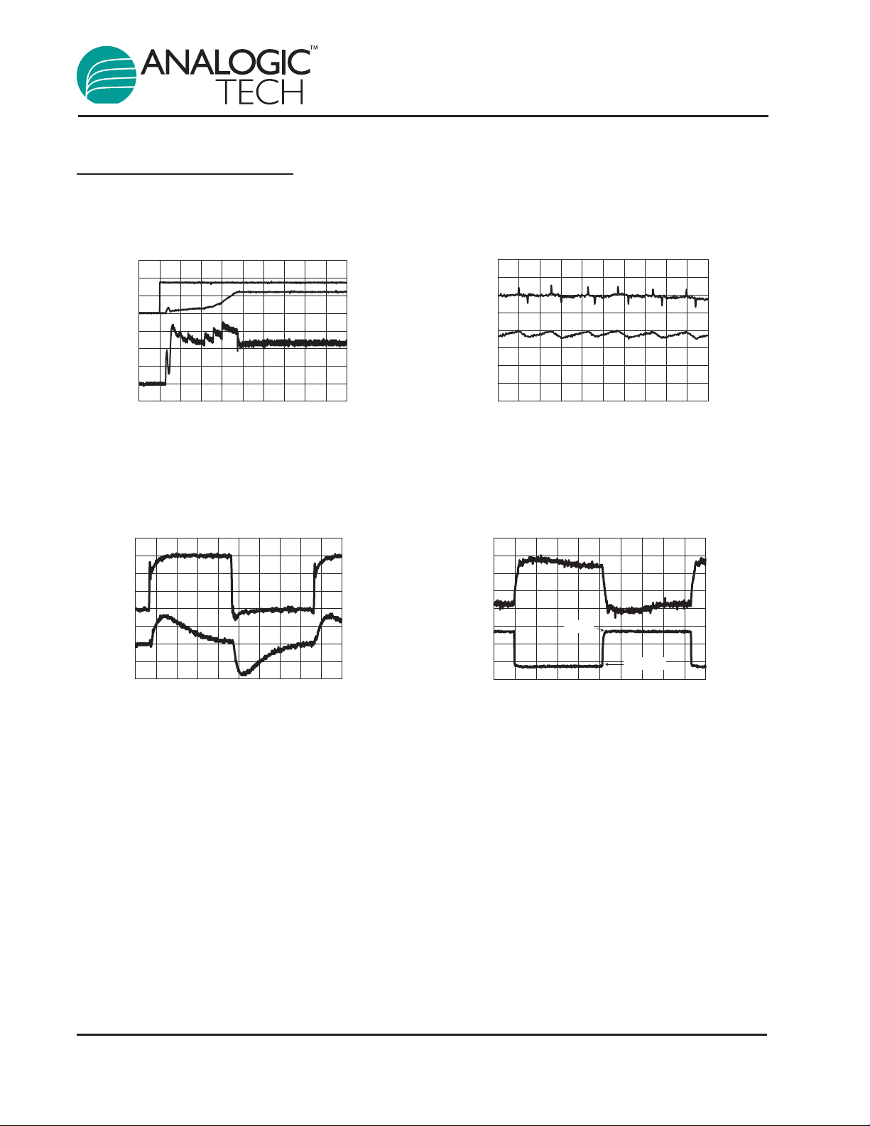
Typical Characteristics
°
Ω
Ω
µ
No Load Supply Current vs. Input Voltage
A)
Supply Current (µ
)
(mΩ
DSON
R
300
250
200
150
100
50
200
180
160
140
120
100
80
60
40
20
85°C
-40°C
0
2.5 3 43.5 4.5 5.55
25°C
Input Voltage (V)
P-Channel R
vs. Input Voltage
DSON
120°C100°C
25°C85°C
0
2.5 3 43.5 4.5 5 5.5
Input Voltage (V)
DC Regulation
(V
= 2.5V)
OUT
2.0
1.0
0.0
-1.0
-2.0
Output Error (%)
-3.0
-4.0
1 10 100 1000 10000
VIN = 3.0V
VIN = 3.3V
Output Current (mA)
N-Channel R
200
180
160
140
)
120
(mΩ
100
80
DSON
R
60
40
20
0
2.5 3 3.5 4 4.5 5 5.5
Input Voltage (V)
VIN = 3.6V
vs. Input Voltage
DSON
25°C85°C
120°C100°C
Output Voltage vs. Temperature
(VIN = 3.6V; V
0.1
0
-0.1
-0.2
-0.3
-0.4
-0.5
-0.6
Output Voltage Error (%)
-0.7
-40 -20 0 20 40 60 80 100
= 2.5V; I
OUT
Temperature (°
OUT
C)
= 1.0A)
1.3
1.28
1.26
1.24
1.22
Frequency (MHz)
1.2
2.7 3.1 3.5 3.9 4.3 4.7 5.1 5.5
Frequency vs. Input Voltage
(V
= 1.8V)
OUT
Input Voltage (V)
AAT1157
1MHz 1.2A Buck DC/DC Converter
6 1157.2005.11.1.4
Typical Characteristics
(V
= 2.5V; I
OUT
6.0
4.0
2.0
0.0
-2.0
(top) (V)
-4.0
-6.0
-8.0
Enable and Output Voltage
-10.0
OUT
Time (250µµs/div)
Line Transient
(I
= 1.2A; VO = 2.5V)
OUT
4.4
4.2
4.0
3.8
3.6
3.4
(top) (V)
Input Voltage
3.2
3.0
2.8
Time (25µµs/div)
Soft Start
= 1.2A; VIN = 3.6V)
3.5
3.0
2.5
2.0
1.5
1.0
0.5
0.0
-0.5
0.24
0.20
0.16
0.12
0.08
0.04
0.00
-0.04
-0.08
(V
0.02
Inductor Current
(bottom) (A)
0.01
0
-0.01
-0.02
-0.03
(top) (V)
-0.04
-0.05
-0.06
Output Voltage (AC coupled)
(400mA-1.2A; VIN = 3.3V; V
Output Voltage (AC coupled)
(bottom) (V)
0.08
0.05
0.02
-0.01
-0.04
-0.07
(V) (top)
-0.10
-0.13
-0.16
Output Voltage (AC Coupled)
Output Ripple
= 2.5V; I
OUT
= 1.2A; VIN = 3.6V)
OUT
Time (500ns/div)
Load Transient Response
= 2.5V)
OUT
1.2A
400mA
Time (20µµs/div)
3
2.5
(bottom) (A)
2
1.5
1
0.5
0
4.0
3.5
3.0
(A) (bottom)
2.5
2.0
1.5
1.0
0.5
0.0
Inductor Current
Load Current

AAT1157
1MHz 1.2A Buck DC/DC Converter
1157.2005.11.1.4 7
Functional Block Diagram
Applications Information
Control Loop
The AAT1 157 is a peak current mode buck converter .
The inner wide bandwidth loop controls the inductor
peak current. The inductor current is sensed through
the P-channel MOSFET (high side) and is also used
for short-circuit and overload protection. Afixed slope
compensation signal is added to the sensed current
to maintain stability for duty cycles greater than 50%.
The loop appears as a voltage-programmed current
source in parallel with the output capacitor.
The voltage error amplifier output programs the
current loop for the necessary inductor current to
force a constant output voltage for all load and line
conditions. The external voltage feedback resistive
divider divides the output voltage to the error amplifier reference voltage of 0.6V. The low-DC gain
voltage error amplifier eliminates the need for
external compensation components while providing sufficient DC loop gain for good load regulation.
The voltage loop crossover frequency and phase
margin are set by the output capacitor.
Soft Start/Enable
Soft start increases the inductor current limit point
in discrete steps once the input voltage or enable
input is applied. It limits the current surge seen at
the input and eliminates output voltage overshoot.
When pulled low, the enable input forces the
AAT1157 into a non-switching shutdown state.
The total input current during shutdown is less
than 1µA.
Power and Signal Source
Separate small signal ground and power supply
pins isolate the internal control circuitry from the
noise associated with the output power MOSFET
switching. The low-pass filter R1 and C2 shown in
the Figure 1 schematic filters the input noise associated with the power switching.
Current Limit and Over-Temperature
Protection
For overload conditions, the peak input current
sensed through the high-side P-channel MOSFET
is limited. Thermal protection completely disables
switching when internal dissipation becomes
excessive, protecting the device from damage. The
junction over-temperature threshold is 140°C with
15°C of hysteresis. Once the over-temperature or
over-current fault is removed, the AAT1157 automatically recovers.
1.0V REF
1MΩ
OSC
OP. AMP
Temp.
Sensing
FB
CC
CMP
LOGIC
ENSGND PGND
VP = 2.7V to 5.5VV
DH
LX
DL

AAT1157
1MHz 1.2A Buck DC/DC Converter
8 1157.2005.11.1.4
Inductor
The output inductor should limit the ripple current to
330mA at the maximum input voltage. This matches the inductor current downslope with the fixed
internal slope compensation. For a 2.5V output and
the ripple set to a maximum input voltage of 4.2V,
the inductance value required to limit the ripple current to 330mAis 3.0µH. From this calculated value,
a standard value can be selected.
Manufacturer's specifications list both the inductor
DC current rating, which is a thermal limitation, and
the peak current rating, which is determined by the
saturation characteristics. The inductor should not
show any appreciable saturation under normal load
conditions. Some inductors may meet the peak and
average current ratings yet result in excessive losses due to a high DCR. Always consider the losses
associated with the DCR and its effect on the total
converter efficiency when selecting an inductor.
For a maximum ripple current of 330mA, the peak
switch and inductor current at 1.2Ais 1.365A. Astandard value of 3.0µH can be used in this example. The
3.0µH Sumida series CDRH5D28 inductor has a
24mΩ maximum DCR and a 2.4A DC current rating.
Input Capacitor
The primary function of the input capacitor is to provide a low impedance loop for the edges of pulsed
current drawn by the AAT1157. A low ESR/ESL
ceramic capacitor is ideal for this function. To minimize stray inductance, the capacitor should be
placed as closely as possible to the IC. This keeps
the high frequency content of the input current
localized, minimizing radiated and conducted EMI
while facilitating optimum performance of the
AAT1157. Ceramic X5R or X7R capacitors are
ideal for this function. The size required will vary
depending on the load, output voltage, and input
voltage source impedance characteristics. Values
range from 1µF to 10µF. The input capacitor RMS
current varies with the input voltage and the output
voltage. The equation for the RMS current in the
input capacitor is:
The input capacitor RMS ripple current reaches a
maximum when VINis two times the output voltage where it is approximately one half of the load
current. Losses associated with the input ceramic
capacitor are typically minimal and are not an
issue. The proper placement of the input capacitor can be seen in the evaluation board layout (C1
in Figure 2).
Figure 1: AAT1157 Evaluation Board Schematic
Lithium-Ion to 2.5V Converter.
VIN+
C1
10µF
Enable
R1
100
R2
100K
C2
0.1µF
C1 Murata 10µF 6.3V X5R GRM42-6X5R106K6.3
C3,C4 MuRata 22µF 6.3V GRM21BR60J226ME39L X5R 0805
L1 Sumida CDRH5D28-3R0NC
U1
AAT1157
12
VP
VP
VP
EN
VCC
N/C
N/C
SGND
FB
LX
LX
LX
N/C
PGND
PGND
PGND
11
10
7
9
6
8
5
OUT
⋅ F
⎛
V
⎝
V
V
V
L = ⋅ 1 -
∆I
PP
2.5
= ⋅ 1 -
0.33A ⋅ 1MHz
= 3.07µH
OUT
IN(MAX)
⎞
⎠
2.5V
4.2V
⎞
⎠
⎛
⎝
LX
4
15
14
L1
3.0µH
13
16
3
2
1
R4
59.0k
V
+
OUT
V
(V) R3 (kΩ)
R3
C3-C4
2x 22µF
GNDGND
OUT
0.8 19.6
0.9 29.4
1.0 39.2
1.1 49.9
1.2 59.0
1.3 68.1
1.4 78.7
1.5 88.7
1.8 118
2.0 137
2.5 187
3.3 267
V
I
= IO ⋅ ⋅ 1 -
RMS
O ⎛ VO
V
⎝ V
IN
IN
⎞
⎠

AAT1157
1MHz 1.2A Buck DC/DC Converter
1157.2005.11.1.4 9
Output Capacitor
Since there are no external compensation components, the output capacitor has a strong effect on loop
stability. Larger output capacitance reduces the
crossover frequency while increasing the phase margin. For the 2.5V 1.2A design using the 3.0µH inductor, a 40µF cap acitor provides a stable output. Table 1
provides a list of suggested output capacitor values
for various output voltages. In addition to assisting in
stability, the output capacitor limits the output ripple
and provides holdup during large load transitions. The
output capacitor RMS ripple current is given by:
For an X7R or X5R ceramic capacitor, the ESR is
very low and the dissipation due to the RMS current
of the capacitor is not a concern. Tantalum capacitors with sufficiently low ESR to meet output voltage
ripple requirements also have an RMS current rating
well beyond that actually seen in this application.
Layout
Figures 2 and 3 display the suggested PCB layout
for the AAT1157. The following guidelines should
be used to help insure a proper layout.
1. The input capacitor (C1) should connect as
closely as possible to VP(Pins 10, 11, and 12)
and PGND (Pins 1, 2, and 3).
2. C3-C4 and L1 should be connected as closely as possible. The connection from L1 to the
LX node should be as short as possible.
3. The trace connecting the FB pin to resistors R3
and R4 should be as short as possible by placing R3 and R4 immediately next to the
AAT1157. The sense trace connection R3 to
the output voltage should be separate from any
power trace and connect as closely as possible
to the load point. Sensing along a high-current
load trace will degrade DC load regulation.
4. The resistance of the trace from the load return to
the PGND (Pins 1, 2, and 3) and SGND (Pin 5)
should be kept to a minimum. This will help to
minimize any error in DC regulation due to differences in the potential of the internal signal
ground and the power ground. SGND (Pin 5) can
also be used to remotely sense the output
ground at the point of load to improve regulation.
5. Alow pass filter (R1 and C2) provides a cleaner bias source for the AAT1157 active circuitry.
C2 should be placed as closely as possible to
SGND (Pin 5) and VCC(Pin 9).
6. For good heat transfer, four 15 mil vias spaced
on a 26 mil grid connect the QFN central paddle to the bottom side ground plane, as shown
in Figures 2 and 3.
Thermal Calculations
There are three types of losses associated with the
AAT1157: MOSFET switching losses, conduction
losses, and quiescent current losses. The conduction losses are due to the R
DSON
characteristics of
the internal P- and N-channel MOSFET power
devices. At full load, assuming continuous conduction mode (CCM), a simplified form of the total losses is given by:
Figure 2: Evaluation Board Top Side. Figure 3: Evaluation Board Bottom Side.
V
I
RMS
1
=
2
⋅
3
⋅
⋅ (VIN - V
OUT
L ⋅ F ⋅ V
)
OUT
IN

AAT1157
1MHz 1.2A Buck DC/DC Converter
10 1157.2005.11.1.4
Where IQis the AAT1157 quiescent current.
Once the total losses have been determined, the
junction temperature can be derived from the θJAfor
the QFN package. Close attention should be paid to
the proper layout for the QFN package. Proper size
and placement of thermal routing vias below the
central paddle is necessary for good heat transfer to
other PCB layers and their ground planes. The θ
JA
for the QFN package with no connection to the central paddle is 50°C/W. The actual θJAwill vary with
the number and type of vias. The PCB board size,
number of board layers, and ground plane characteristics also influence the θJA. Agood thermal connection from the paddle to the PCB ground plane
layers can significantly reduce θJA.
Adjustable Output
Resistors R3 and R4, as shown in Figure 1, force
the output to regulate higher than the 0.6V reference voltage level. The optimum value for R4 is
59kΩ. Values higher than this can cause stability
problems, while lower values can degrade light
load efficiency. For a 2.5V output with R4 set to
59kΩ, R3 is 187kΩ.
Table 1: Suggested Component Values.
Buck-Boost Output
Figure 4 shows how to configure the AAT1157 in a
buck boost configuration with an external MOSFET
and Schottky diode. The converter has a 3.3V
600mA output with an input voltage ranging from
2.7V to 5.5V.
Output Output R3 for
Voltage L1 Capacitor R4 = 59k
ΩΩ
(V) (µH) (C3-C4) (µF) (kΩΩ)
0.8 1.5 - 2.6 3x 22 19.6
1.0 1.5 - 3.3 2x 22 39.2
1.2 2.2 - 3.3 2x 22 59
1.5 2.2 - 4.7 2x 22 88.7
1.8 3.0 - 4.7 2x 22 118
2.5 3.0 - 4.7 2x 22 187
3.3 2.2 - 4.7 22 267
Figure 4: AAT1157 Buck Boost Converter.
2
I
⋅ (R
O
P =
+ (tsw ⋅ F ⋅ IO ⋅ VIN + IQ) ⋅ V
DSON(HS)
⋅ VO + R
V
IN
DSON(LS)
IN
⋅ (V
- VO))
IN
TJ= P · ΘJA + T
AMB
V
⎛⎞
R3 = -1 · R4 = - 1 · 59kΩ = 187kΩ
O
V
⎝⎠
REF
2.5V
⎛⎞
0.6V
⎝⎠
VIN 2.7V to 5.5V
C1
22µF
R1
100
C2
0.1µF
L1 Sumida CDRH5D28-3R0
C1 Mu rat a 22µF 10V X7R 1210 GRM32ER71A226KE20L
C3,C4 MuRata 22µF 6.3V X5R 0805 GRM21BR60J226ME39L
12
11
10
7
9
6
8
5
U1
AAT1157
VP
VP
VP
EN
VCC
N/C
N/C
SGND
OUT
LX
LX
LX
N/C
PGND
PGND
PGND
R2
R3
59.0k
267k
L1
3.0µH
4
15
14
13
16
3
2
1
VO 3.3V/600mA
D1
MBRM120L
Q1
Si2302ADS
C3,C4
2x 22µF

AAT1157
1MHz 1.2A Buck DC/DC Converter
1157.2005.11.1.4 11
Design Example
Specifications
I
OUT
1.2A
I
RIPPLE
330mA
V
OUT
2.5V
V
IN
3.0V to 4.2V
F
S
1MHz
T
AMB
= 85°C
Maximum Input Capacitor Ripple:
Inductor Selection:
Select Sumida inductor CDRH5D28 3.0µH.
Output Capacitor Ripple Current:
II
VV
⎛⎞
OO
=· · -=
RMS O
1 0.59Arms
⎝⎠
VV
IN IN
P = esr · I
2
= 5mΩ · 0.592 A = 1.7mW
RMS
⋅ F
⎛
V
⎝
V
∆I
OUT
PP
L = ⋅ 1 - = ⋅ 1 - = 3.07µH
VO
V
⎛
∆I = ⋅ 1 - = ⋅ 1- = 340mA
L ⋅ F
IPK = I
P = I
O
⎝
+ ∆I = 1.2A + 0.17A = 1.37A
OUT
2
2
⋅ DCR = (1.2A)2 ⋅ 31mΩ = 45mW
⎞
2.5
OUT
⎠
VIN 0.33A ⋅ 1MHz
2.5
⎞
O
V
3.0µH ⋅ 1MHz
⎠
IN
V
V
⎛
⎝
⎛
⎝
2.5V
4.2V
2.5V
4.2V
⎞
⎠
⎞
⎠
(V
I
RMS
1
=·
·
23
OUT
) · (VIN - V
LFV
··
)
OUT
IN
1 2.5V · (4.2V - 2.5V)
=
· = 97.4mArms
3.0µH · 1MHz · 4.2V
·
23
Pesr = esr · I
2
= 5mΩ · (97.4mA)2 = 47.4µW
RMS

AAT1157
1MHz 1.2A Buck DC/DC Converter
12 1157.2005.11.1.4
AAT1157 Dissipation and Junction Temperature Estimate:
Surface Mount Inductors
Surface Mount Capacitors
Value Voltage
Manufacturer Part Number (µF) (V) Temp. Co. Case
MuRata GRM21BR60J106ME01L 10 6.3 X5R 0805
MuRata GRM21BR60J226ME01L 22 6.3 X5R 0805
MuRata GRM31CR60J106KA01L 10 6.3 X5R 1206
Value Max DC DCR Size (mm)
Manufacturer Part Number (µH) Current (A) (mΩΩ) L x W x H Type
Sumida CDRH5D28-2R6 2.6 2.6 18 5.7x5.7x3.0 Shielded
Sumida CDRH5D28-3R0 3.0 2.4 24 5.7x5.7x3.0 Shielded
Sumida CDRH5D28-4R2 4.2 2.2 31 5.7x5.7x3.0 Shielded
TaiyoYuden NPO5DB4R7M 4.7 1.4 38 5.9x6.1x2.8 Shielded
Sumida CDRH4D28-2R2 2.2 2.04 31 5.0x5.0x3.0 Shielded
Sumida CDRH4D28-2R7 2.7 1.6 43 5.0x5.0x3.0 Shielded
Sumida CDRH4D28-3R3 3.3 1.57 49 5.0x5.0x3.0 Shielded
Sumida CDRH5D18-4R1 4.1 1.95 57 5.7x5.7x2.0 Shielded
Sumida CDRH3D16/HP-2R2 2.2 2.3 59 4.0x4.0x1.8 Shielded
Sumida CDRH3D16/HP-3R3 3.3 1.8 85 4.0x4.0x1.8 Shielded
MuRata LQH55DN4R7M03 4.7 2.7 41 5.0x5.0x4.7 Non-Shielded
MuRata LQH66SN4R7M03 4.7 2.2 25 6.3x6.3x4.7 Shielded
2
I
· (R
=
=
O
2
1.2A
· (0.17Ω · 2.5V + 0.16Ω · (4.2V - 2.5V))
P
TOTAL
= 341mW
T
= T
J(MAX)
AMB
+ Θ
DSON(HS)
· P
JA
· VO + R
V
IN
DSON(LS)
· (VIN -VO))
+ (tsw · F · IO + IQ) · V
4.2V
= 85°C + 50°C/W · 0.341W = 102°C
TOTAL
IN
+ (20nsec · 1MHz · 1.2A + 275µA) · 4.2V

AAT1157
1MHz 1.2A Buck DC/DC Converter
1157.2005.11.1.4 13
Ordering Information
Package Information
QFN33-16
All dimensions in millimeters.
Output Voltage Package Marking
1
Part Number (Tape and Reel)
2
FB = 0.8V, Adjustable ≥ 0.8V QFN33-16 OEXYY AAT1157IVN-T1
1. XYY = assembly and date code.
2. Sample stock is generally held on part numbers listed in BOLD.
All AnalogicTech products are offered in Pb-free packaging. The term “Pb-free” means
semiconductor products that are in compliance with current RoHS standards, including
the requirement that lead not exceed 0.1% by weight in homogeneous materials. For more
information, please visit our website at http://www.analogictech.com/pbfree.
0.230 ± 0.05
1
5
1.55 ± 0.15
9
Pin 1 Dot By Marking
3.000 ± 0.05
Top View
Pin 1 Identification
3.000 ± 0.05
13
0.400 ± 0.05
0.500 ± 0.05
Bottom View
0.850 ± 0.05
0.025 ± 0.025
0.203 ± 0.0254
Side View

AAT1157
1MHz 1.2A Buck DC/DC Converter
14 1157.2005.11.1.4
Advanced Analogic Technologies, Inc.
830 E. Arques Avenue, Sunnyvale, CA 94085
Phone (408) 737-4600
Fax (408) 737-4611
© Advanced Analogic Technologies, Inc.
AnalogicTech cannot assume responsibility for use of any circuitry other than circuitry entirely embodied in an AnalogicTech product. No circuit patent licenses, copyrights, mask work rights,
or other intellectual property rights are implied. AnalogicTech reserves the right to make changes to their products or specifications or to discontinue any product or service without notice.
Customers are advised to obtain the latest version of relevant information to verify, before placing orders, that information being relied on is current and complete. All products are sold
subject to the terms and conditions of sale supplied at the time of order acknowledgement, including those pertaining to warranty, patent infringement, and limitation of liability. AnalogicT ech
warrants performance of its semiconductor products to the specifications applicable at the time of sale in accordance with AnalogicTech’s standard warranty. Testing and other quality control techniques are utilized to the extent AnalogicTech deems necessary to support this warranty. Specific testing of all parameters of each device is not necessarily performed.
 Loading...