

Evaluation Board User Guide
UG-416
S/PDIF
INTERFACE
DSP
INTERFACE
CONTROL
INTERFACE
CLOCK
AND
DATA
ROUTING
DAC 9 TO
DAC 16
DAC 1 TO
DAC 8
POWER SUPPLY
ADAU1966
10717-001
One Technology Way • P. O. Box 9106 • Norwood, MA 02062-9106, U.S.A. • Tel: 781.329.4700 • Fax: 781.461.3113 • www.analog.com
Evaluating the ADAU1966 High Performance,
Low Power, Multibit Sigma-Delta DAC
EVAL-ADAU1966Z PACKAGE CONTENTS
ADAU1966 evaluation board
USBi control interface board
USB cable
D-sub 25-pin to (8) XLR male
12 V desktop supply
OTHER SUPPORTING DOCU M ENTATION
ADAU1966 data sheet
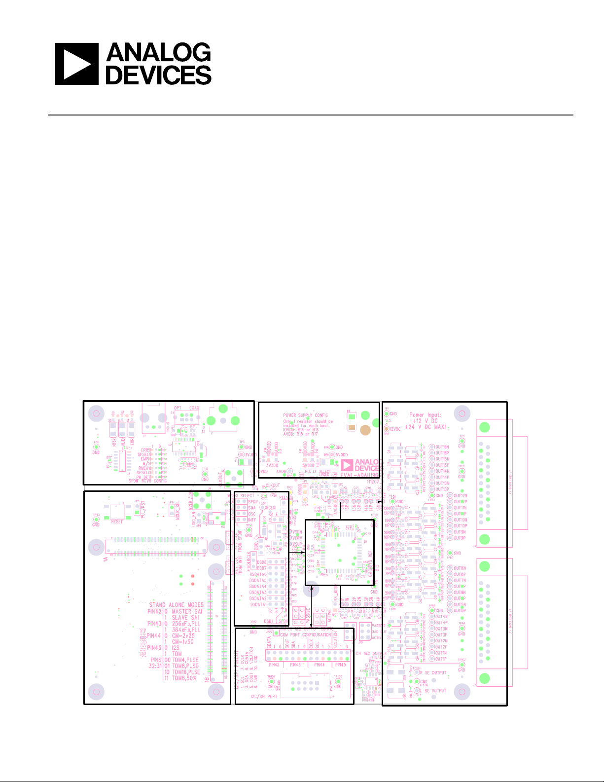
EVALUATION BOARD OVERVIEW
This document explains the design and setup of the evaluation
board for the ADAU1966. The evaluation board must be connected
to an external 12 V dc power supply and ground; the board draws
approximately 150 mA. On-board regulators derive 9 V, 5 V,
and 3.3 V supplies for the ADAU1966 and peripherals. The
ADAU1966 can be controlled through either an I
2
C or SPI
FUNCTIONAL BLOCK DIAGRAM
interface. A small external interface board, EVAL -ADUSB2EBZ,
also called USBi, connects to a PC USB port and provides either
2
I
C or SPI access to the evaluation board through a ribbon cable. A
graphical user interface (GUI) program, the Automated Register
Window Builder, is provided for easy programming of the chip
in a Microsoft® Windows® PC environment. The evaluation
board allows demonstration and performance testing of most
ADAU1966 features, including high performance digital-to-
analog converter (DAC) operation.
The board has an S/PDIF receiver with RCA and optical
connectors, as well as a discrete serial audio interface that is
available on the Analog Devices, Inc. system development
platform (SDP) interface. Analog outputs are accessible with two
D-sub, 25-pin connectors using the professional audio standard. A
single D-sub, 25-pin to XLR male cable is included with the board
for connecting individual DAC channels to an audio system.
PLEASE SEE THE LAST PAGE FOR AN IMPORTANT
WARNING AND LEGAL TERMS AND CONDITIONS.
Figure 1.
Rev. 0 | Page 1 of 28

UG-416 Evaluation Board User Guide
TABLE OF CONTENTS
EVAL-ADAU1966Z Package Contents .......................................... 1
Other Supporting Documentation ................................................. 1
Evaluation Board Overview ............................................................ 1
Functional Block Diagram .............................................................. 1
Revision History ............................................................................... 2
Setting Up the Evaluation Board .................................................... 3
Standalone Mode .......................................................................... 3
I2C and SPI Control ...................................................................... 4
Automated Register Window Builder Software Installation .. 4
Hardware Setup—USBi ............................................................... 4
REVISION HISTORY
5/12—Revision 0: Initial Version
Powering the Board .......................................................................5
Reset for the Evaluation Board ....................................................5
Setting Up the Master Clock (MCLK) ........................................6
Crystal Operation ..........................................................................6
PLL Selection .................................................................................7
Digital Audio Connections and Routing ...................................7
Connecting Analog Audio Cables ..............................................8
Using the ADAU1966 ....................................................................8
Schematics and Artwork ..................................................................9
Rev. 0 | Page 2 of 28
Evaluation Board User Guide UG-416
10717-002
10717-003
SETTING UP THE EVALUATION BOARD
STANDALONE MODE
The ADAU1966 has a standalone mode that allows the user to
choose between a limited number of operation modes without
the need for a control interface. Applying a jumper across JP21,
as shown in Figure 2, pulls SA_MODE (Pin 46) high, enabling
the standalone mode in the ADAU1966. The SA_MODE selections
are listed in Tab le 1.
Table 1. Standalone Modes
Pin(s) Jumper Setting Description
42 0 Serial audio interface, master mode
1 Serial audio interface, slave mode
43 0 MCLK select: 256 × fS, PLL
1 MCLK select: 384 × fS, PLL
44 0 CM = 2.25 V (for AVDD = 5 V)
1 CM = 1.50 V (for AVDD = 3.3 V)
45 0 Serial audio interface, I2S mode
1 Serial audio interface, TDM mode
32:31 00 TDM4, pulse
01 TDM8, pulse
10 TDM16, pulse
11 TDM8, 50% duty
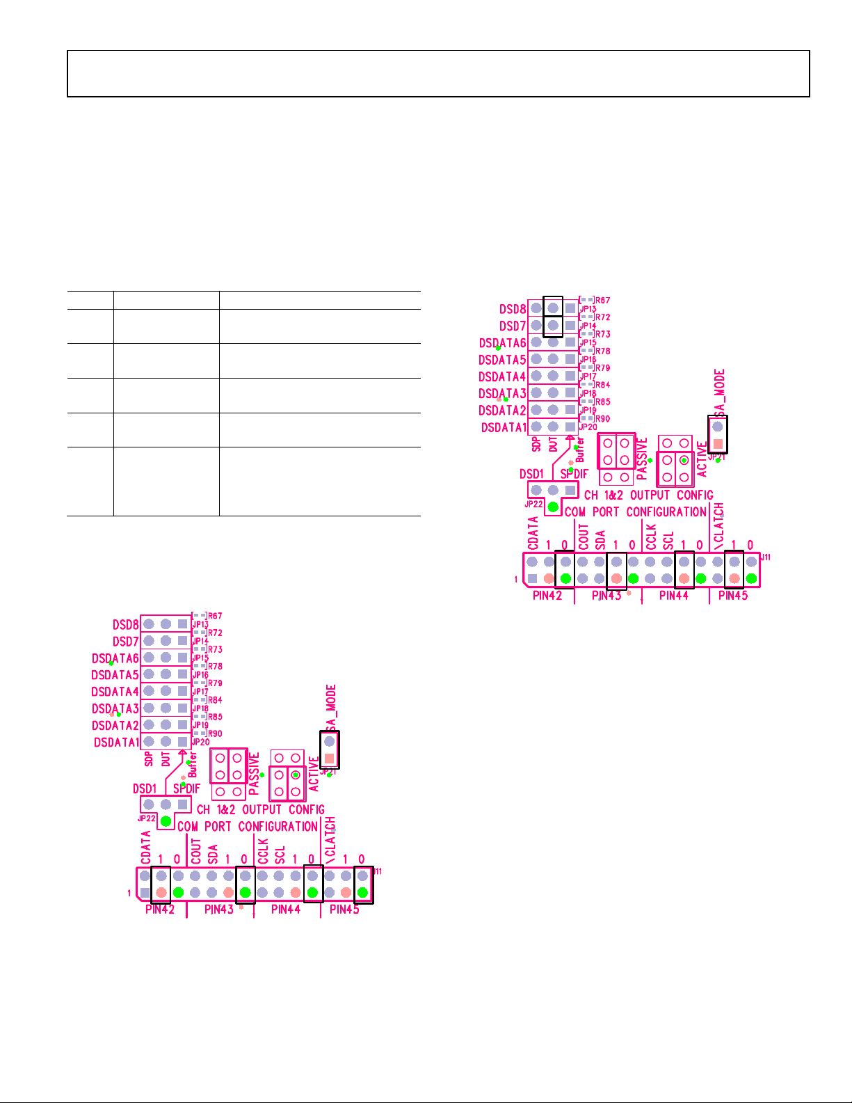
On the E VA L -ADAU1966Z evaluation board, each of the four
ADAU1966 control port pins is brought to a block of jumpers,
allowing each pin to be assigned to either the I
port. In standalone mode, these jumpers can connect the individual
pins to high or low to put the ADAU1966 in the desired mode.
Figure 2. SA_MODE—Slave, 256 × f
2
C port or the SPI
, CM = 2.25 V, I2S
S
The E VA L -ADAU1966Z arrives configured for S/PDIF input.
The S/PDIF receiver operates as a clock master, putting out an
2
I
S stream at 256 × fS. For a quick startup, the ADAU1966 is in
standalone mode with the settings shown in Figure 2. Pin 42 is
pulled high (1) and Pin 43 to Pin 45 are pulled low (0). According
to Table 1, this puts the ADAU1966 in slave mode, running at
256 × f
, while common mode (CM) is set to 2.25 V and the audio
S
serial port is in I
2
S mode. Notice in Figure 2 that the jumper for
Pin 42 is assigned to 1 and that the other pins are assigned to 0.
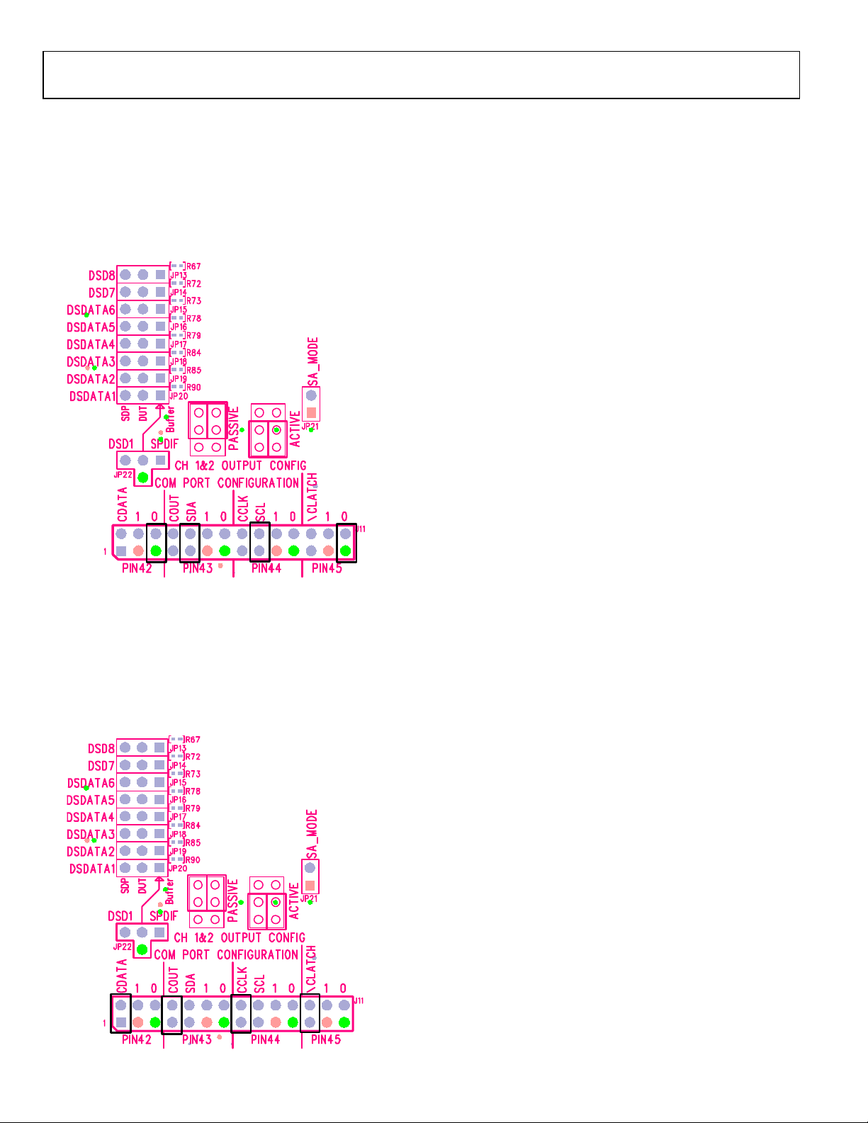
Figure 3. SA_MODE—Master, 384 × f
, CM = 1.50 V, TDM
S
Figure 3 shows the other options for each SA_MODE configuration
pin; master mode, running at 384 × f
, CM set to 1.50 V, and the
S
audio serial port in TDM mode. In the case where the ADAU1966
is put in TDM mode, Pin 31 and Pin 32 can be pulled high or
low to achieve the modes listed in Tabl e 1. The correct pins are
outlined in the top left corner of Figure 3, as DSD8 and DSD7.
Rev. 0 | Page 3 of 28
UG-416 Evaluation Board User Guide
10717-004
10717-005
I2C AND SPI CONTROL
The evaluation board can be configured for live control over
the registers in the ADAU1966. When the Automated Register
Window Builder software is installed and the USBi control
interface is plugged into the board, the software can control
the ADAU1966. For this configuration, the ADAU1966 must
be assigned to I
correct jumper positions.
The Automated Register Window Builder controls the
ADAU1966 and is available for download under the Tool s,
Software, & Simulation Models section of the ADAU1966
product page at www.analog.com/ADAU1966.
In addition, the ADAU1966 can be put into SPI mode for
control by other means. See Figure 5 for the correct jumper
positions.
2
C mode using Address 00. See Figure 4 for the
2
Figure 4. ADAU1966 I
C Control, Address 00
AUTOMATED REGISTER WINDOW BUILDER SOFTWARE INSTALLATION
The Automated Register Window Builder is a program that
launches a graphical interface for direct, live control of the
ADAU1966 registers. The GUI content for a specific part is
defined in a part-specific .xml file; these files are included in
the software installation. To install the Automated Register
Window Builder software, follow these steps:
1. Go to the ADAU1966 product page and download the 64-
Bit OS (ARWB_64BIT.zip) or 32-Bit OS (ARWB_32Bit.zip)
file, which can be found under the Tools, Software, &
Simulation Models section of the ADAU1966 product page.
2. Open the downloaded.zip file and extract the files to an
empty folder on your PC.
3. Install the Automated Register Window Builder by
double-clicking setup.exe and following the prompts. A
computer restart is not required.
4. Copy the .xml file for the ADAU1966 from the extraction
folder into the C:\ProgramFiles\Analog Devices Inc\
AutomatedRegWin folder, if it is not already installed.
HARDWARE SETUP—USBi
To set up the USBi hardware, follow these steps:
1. Plug the USBi ribbon cable into J12, the I
2. Connect the USB cable to the PC and to the USBi.
3. When prompted for drivers, follow these steps:
a. Choose Install from a list or a specific location.
b. Choose Search for the best driver in these locations.
c. Check the box for Include this location in the search.
d. Find the USBi driver C:\Program Files\Analog
Devices Inc\AutomatedRegWin\USB drivers.
e. Click Next.
f. If prompted to choose a driver, select CyUSB.sys.
g. If the PC is running Windows XP and a message
appears saying that the software has not passed
Windows logo testing, click Continue Anyway.
4. Open the Automated Register Window Builder application
and load the .xml file for the part on the evaluation board.
Plug the 10-way ribbon cable on the USBi into the I
port (J12) on the evaluation board.
2
C/SPI port.
2
C/SPI
Figure 5. ADAU1966 SPI Control
Rev. 0 | Page 4 of 28
Evaluation Board User Guide UG-416
10717-006
10717-007
10717-008
10717-009
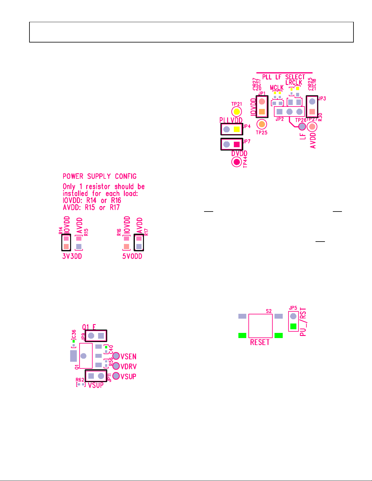
POWERING THE BOARD
The E VA L -ADAU1966Z evaluation board requires a power
supply input of 12 V dc and ground to the power jack; 12 V
draws ~150 mA at higher sample rates with all channels running.
The on-board regulators provide 9.0 V, 5.0 V, and 3.3 V rails. The
9.0 V rail is derived from 12 V by a linear regulator; it provides
voltage to the audio op amp in the active output filter for
Channel 1 and Channel 2. The 5.0 V rail is derived from 12 V
by a switching regulator; it can supply AVDD as well as IOVDD
for the ADAU1966 and other peripherals. The 3.3 V rail is derived
from the 5.0 V supply by an LDO linear regulator; it provides
voltage to AVDD and IOVDD as well as other active peripherals.
AVDD and IOVDD are selected on the board using 0 Ω, 0805
package resistors. Install only one resistor for each load, AVDD
and IOVDD, as described in Figure 6. Figure 6 shows AVDD
fed from 5.0 V and IOVDD fed from 3.3 V.
Figure 6. AVDD and IOVDD Selection Resistors
The ADAU1966 has an internal voltage regulator that allows
the user to derive DVDD and PLLVDD from the AVDD voltage
source. The external PNP transistor, Q1, and passives, C36, C40
and R56, make the regulator circuit shown in Figure 7. Short
both JP9 and JP11 to activate the circuit; JP9 supplies the emitter
of the PNP, and JP11 powers the VSUPPLY pin (Pin 25) on the
ADAU1966.
Links are provided along each ADAU1966 power rail to give access
for current measurement (see Figure 8). These links also allow
directly supplying voltage from an outside source.
Figure 8. ADAU1966 Power Links
RESET FOR THE EVALUATION BOARD
The EVAL -ADAU1966Z has provision for resetting and powering
down the ADAU1966. S2 on the evaluation board, shown in
Figure 9, is a momentary reset switch that pulls the master reset
MR
(
) line low; this line controls the reset generator U10. MR is
also connected to the USBi and SDP INTF connectors through
steering diodes and protection resistors so that outside devices
can control the reset state of the evaluation board, as shown in
Figure 26. The power down jumper, JP5, allows the MR line to be
tied low. The output of the reset generator drives the PU_/RST line.
The PU_/RST line is directly connected to two devices: the S/PDIF
receiver and the ADAU1966. A pull-down resistor holds the line
low until the reset generator, U10, asserts the line high, as shown in
Figure 26. The PU_/RST line is also connected to a pin on the
SDP INTF through a steering diode and protection resistor,
allowing external reset control.
Figure 9. Reset Switch and Power-Down Jumper
Figure 7. ADAU1966 Internal Regulator Jumpers
Rev. 0 | Page 5 of 28
UG-416 Evaluation Board User Guide
10717-011
10717-012
10717-013
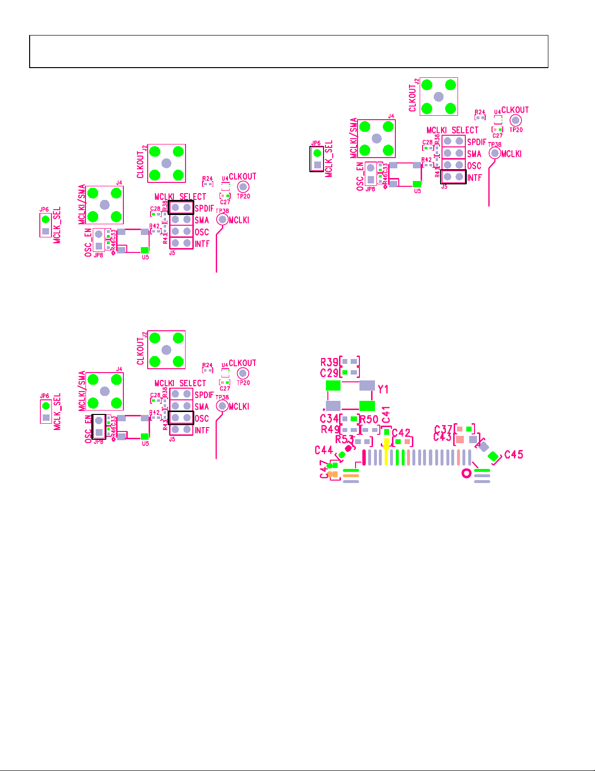
SETTING UP THE MASTER CLOCK (MCLK)
The MCLK routing on the evaluation board is handled by a block
of jumpers, J5, allowing any one of four sources to be selected:
SPDIF, SMA connector, active OSC, and INTF connector. The
board comes with SPDIF selected, as shown in Figure 10.
Figure 10. SPDIF Selected as MCLK Source
The evaluation board has a 12.288 MHz active oscillator that
can be selected by shorting the OSC_EN jumper, JP8, and
selecting OSC on J5, as shown in Figure 11.
Figure 11. Active OSC-Enabled and Selected as MCLK
When using the SDP interface to add serial audio onto the
evaluation board, MCLK can either be supplied by the SDP
board, or it can be supplied by the MCLKO pin of the ADAU1966.
To route MCLK from the SDP interface to the ADAU1966, apply a
shorting jumper across JP6 (MCLK_SEL), as shown in Figure 12;
this sets the direction of the level translators on the board to
receive an MCLK signal from the SDP interface, EI3 1A, Pin 119
(EI3_MCLK), as shown in Figure 28. Next, select INTF on JP5
to route the output of the MCLK level translator to the MCLKI
pin of the ADAU1966.
Figure 12. INTF Input Enabled and Selected
To route MCLK from the ADAU1966 to the SDP interface, remove
the shorting jumper from JP6 (MCLK_SEL); this changes the
direction of the level translators and feeds a buffered version of
10717-010
the MCLKO signal from the ADAU1966 to the EI3_MCLK pin
on the SDP interface.
CRYSTAL OPERATION
The ADAU1966 evaluation board is shipped without R49 on the
board, effectively disabling the crystal circuit. For operation with a
crystal, install a 150 Ω, 0402 resistor and remove any jumpers from
J5. For permanent use of the crystal, remove the 0 Ω resistor, R39.
Figure 13. Crystal Circuit Near ADAU1966
Rev. 0 | Page 6 of 28
Evaluation Board User Guide UG-416
10717-015
10717-017
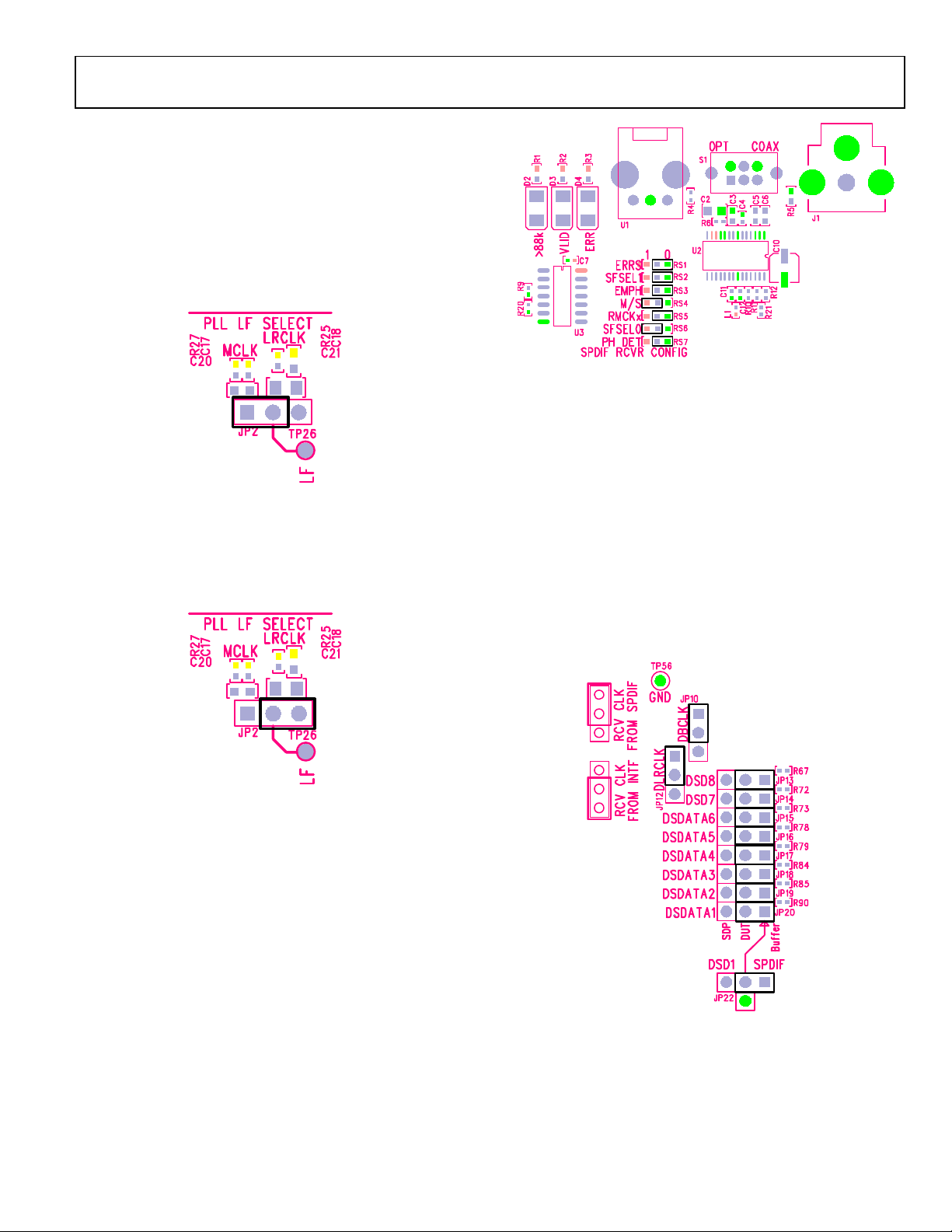
PLL SELECTION
The PLL in the ADAU1966 is very flexible, allowing the part to
run from a wide range of either MCLK or LRCLK frequencies.
It is also possible to shut the PLL off altogether and use the part
in direct MCLK mode; functionality with no PLL is limited to
256 × f
.
S
By default, the ADAU1966 runs from the PLL using MCLK as
the clock source. The MCLK loop filter must be selected using
JP2, as shown in Figure 14.
Figure 16. S/PDIF Input Selector Switch, SW1
A series of resistors is provided to set the functional mode of the
S/PDIF receiver. By default, the S/PDIF receiver runs in master
10717-014
Figure 14. MCLK Selection for PLL Loop Filter
DLRCLK can be selected as the PLL clock source using the PLL
and Clock Control Register 0, Register 0x00, Bits[7:6]. In this
case, the LRCLK loop filter must be selected, as shown in Figure 15.
If DLRCLK is selected as the PLL clock, there is no need for an
MCLK signal.
mode, 256 × f
receiver to make changes to the hardware mode.
The jumpers shown in Figure 17 are set for the S/PDIF receiver
to drive the DBCLK and DLRCLK clock ports and the eight
DSDATA x lines of the ADAU1966. JP22 selects the input to the
buffer; the output of this buffer shows up on the right-hand column
of JP13 to JP20. The pins in the middle column of these jumpers
are connected to the DSDATAx pins of the ADAU1966 through
the appropriate line termination. DBCLK and DLRCLK selections
are made with JP10 and JP12, respectively, where the middle
pins are connected to the DBCLK and DLRCLK pins of the
ADAU1966.
, I2S format; consult the data sheet for the S/PDIF
S
10717-016
Figure 15. LRCLK Selection for PLL Loop Filter
DIGITAL AUDIO CONNECTIONS AND ROUTING
The ADAU1966 evaluation board has two separate inputs for
digital audio signals: S/PDIF and SDP interface.
The S/PDIF receiver can handle either of two options: COAX
uses the RCA jack, J1, and OPT uses the Toslink jack, U1. The
S/PDIF input is selected using S1, as shown in Figure 16.
Figure 17. S/PDIF Data and Clock Routing
The SDP interface, J6 and J8, make up a standard interconnect
within Analog Devices. They provide for transfer of digital audio,
clocks, and control between boards. For additional information,
see the pinout included in the schematic in Figure 28.
Rev. 0 | Page 7 of 28
UG-416 Evaluation Board User Guide
10717-018
10717-019
10717-020
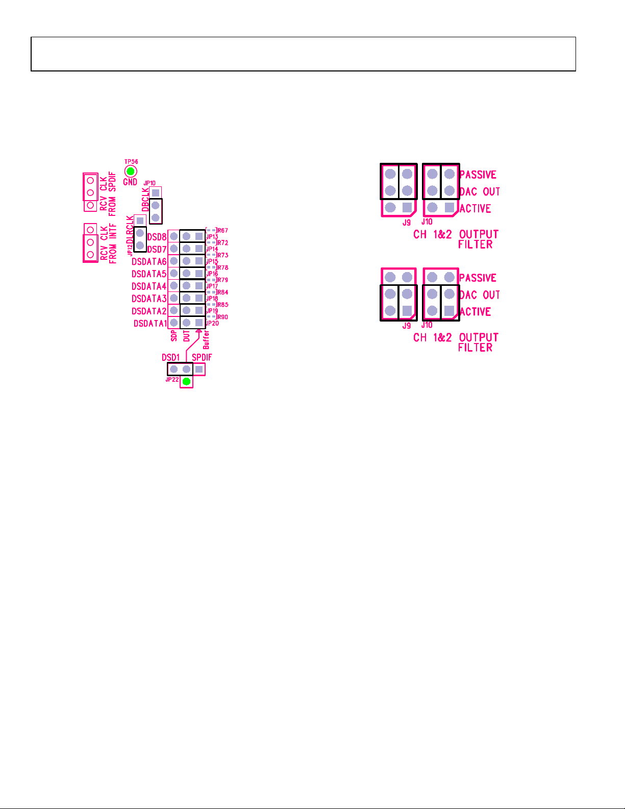
Figure 18 shows the jumpers configuration for using the SDP
interface connector as the digital audio source. JP22 is set so
that the DSDATA1 source from the SDP interface is driving the
buffer, and this buffer is connected to all eight DSDATAx inputs
of the ADAU1966. JP10 and JP12 are set for the ADAU1966 to
run in slave mode from clocks supplied by the SDP interface.
Channel 1 and Channel 2 are also available as single-ended outputs
on a stereo, 3.5 mm stereo jack, J14. The J9 and J10 jumpers assign
the differential outputs of the DAC to either the passive differential
output or the active single-ended filter.
Figure 19 shows J9 and J10 set for the passive differential output
available on the D-sub connector.
Figure 18. SDP Interface DSDATA1 Distribution
CONNECTING ANALOG AUDIO CABLES
There are two forms of the analog outputs of the ADAU1966
evaluation board: differential outputs and single-ended outputs.
The differential outputs appear on through hole test points as well
as on 25-way, female D-sub connectors. The pinout of these D-sub
connectors follows the professional audio standard for eight
differential signals on a single jack. A single 25-pin male D-sub
to XLR male harness has been provided for testing and evaluation
purposes. These cables are widely available on the open market.
The differential outputs of the ADAU1966 drive the connectors
directly through a simple 1-pole RC filter and appropriate ac
coupling.
Figure 19. Channel 1 and Channel 2 in Passive Differential Output Mode
Figure 20. Channel 1 and Channel 2 in Active Single-Ended Output Mode
Figure 20 shows J9 and J10 set for the active single-ended output
available on the 3.5 mm TRS connector, J14.
USING THE ADAU1966
When the ADAU1966 starts in standalone mode, it is operational
upon power up.
If the ADAU1966 is not powered up in standalone mode, the
USBi must be connected to set the appropriate registers to make
the part operational. First, the ADAU1966 must be activated using
the PLL and Clock Control 0 register (Address 0x00) by setting
the PUP bit (Bit 0) to 1 for master power-up. Next, using the
DAC Control 0 register (Address 0x06) set the MMUTE bit (Bit
0) to 0 for normal operation. The ADAU1966 now passes audio
in its default mode: I
If different settings are desired, it is recommended to program
the custom settings before unmuting the part.
2
S, 256 × fS, slave mode, and CM = 2.25 V.
Rev. 0 | Page 8 of 28
Evaluation Board User Guide UG-416
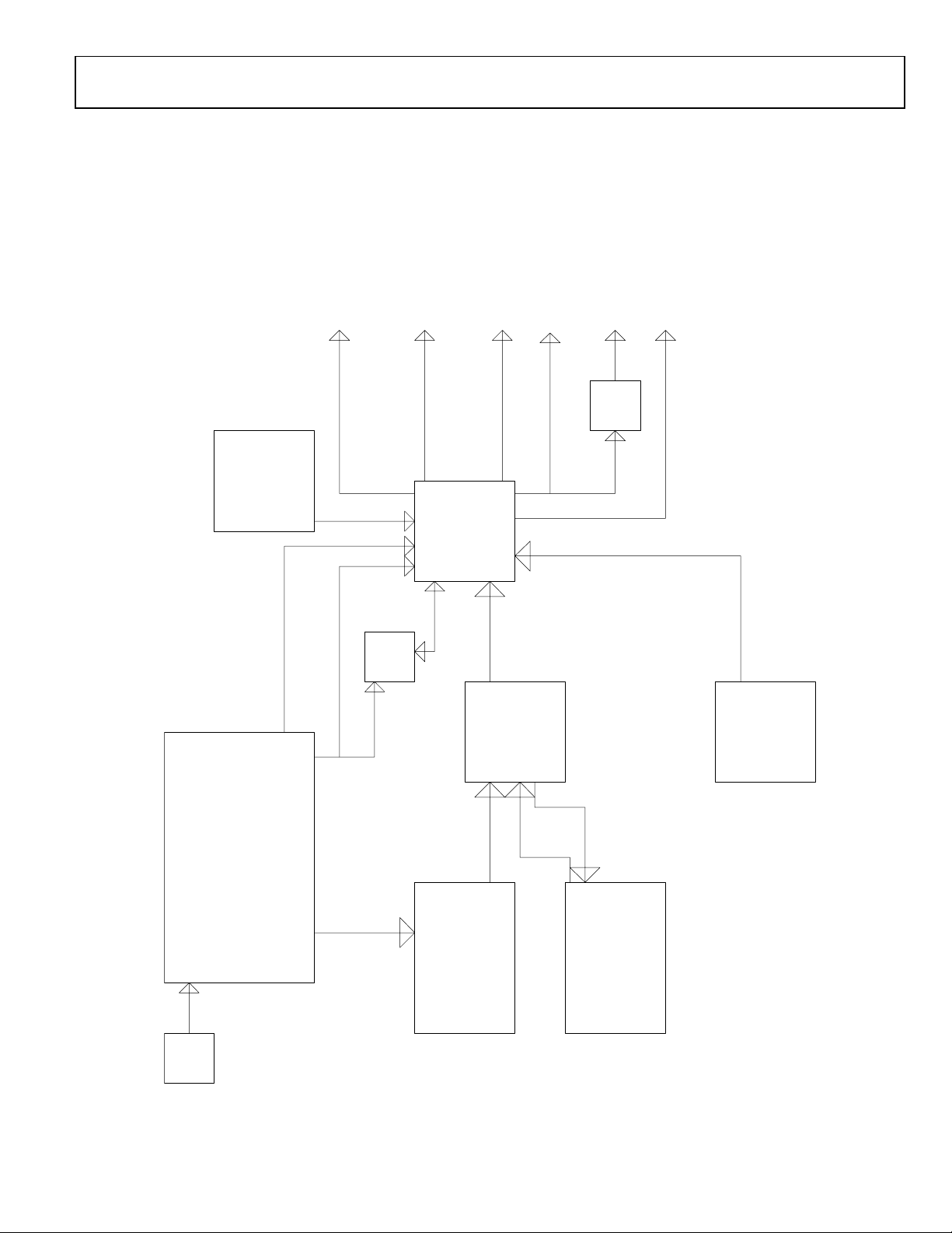
ADAU1966
DAC Diff Out 3-8 Passive RC 1 pole
DAC Diff Out 9-16 Passive RC 1 pole
1 Pole Passive 1 Pole Active
DAC Diff Out 1-2 Passive RC 1 Pole
DAC SE Out 1-2 Active Filter
Power Supply Regulators
5v0 = Switching Supply
3v3 = Linear Supply derived from 5v0
Int Reg
Xistor
DVDD
PLLVDD
AVDD = 5v0 / 3v3
IOVDD = 5v0 / 3v3
Single jumpers for each supply
for current measurement
MCLK Sources
SPDIF
Crystal
DSP Intf
EXT In
Active OSC
USBi Control port
SA_Mode Jumps
COM Port Jumps
PD Jump
SPDIF Receiver
DSP/FPGA Interface
BCLK, LRCLK
SDATA Jumps
with Buffer
12 VDC
Input
Optical and Coax In
Allows for Direct
Connect to DUT
SE output on TRS Mini Jack
Diff Outs on d-sub 25
Reset Switch
3v3 for SPDIF Core
IOVDD comes from DUT IOVDD
Control Jumpers
Hardware Mode
Desktop Supply
CM Output on TP
Buffered MCLKO
OP AMP = 9v0 Linear Adjustable
CLKs
CLKs and DATA
3v3 / 2v5
IOVDD and AVDD select using 0R00
24 VDC Input MAX!
10717-021
SCHEMATICS AND ARTWORK
Figure 21. EVAL-ADAU1966Z Block Diagram Schematic, Page 1
Rev. 0 | Page 9 of 28

UG-416 Evaluation Board User Guide
Enab le
ADAU1966 Voltag e Regulator
MCLK LRCLK
See pages 5&6 for jumpers
Stand-Alone Modes
Master SAI
Slave SAI
256xFs, PLL
382xFs,PLL
CM=2v25
CM=1v50
I2S
TDM
TDM4, Pulse
TDM8, Pulse
TDM16, Pulse
TDM8, 50% Duty Cycle
0101010
1
000110
11
Pin 42
Pin 43
Pin 44
Pin 45
Pins 32:31
C76
0.47uF
C37
C68 C65
C77
C43
0.47uF
C72
0.47uF
C45
0.47uF
C75
C41
C71
C67
C42
C47
C44C53
JP1
JP3
+
C134
10uF
+
C130
10uF
TP66
TP63
TP26
TP21
TP25
TP44
B
C
E
C
Q1
ZX5T953GTA
C36C40
+
C126
10uF
R56
1k50
TP50
TP53
C18
2.2nFNP0
C21
39nF
R25
3k32
BA
JP2
C17
390pF
C20
5.6nF
R27
562R
13579
246810
1113151719
1214161820
2221
2423
2625
27 28
J11
HEADER_28WAY_UNSHROUD
+
C125
10uF
+
C127
10uF
+
C129
10uF
JP11
+
C128
10uF
+
C131
10uF
+
C133
10uF
27
DBCLK28DLRCLK
31
DSDATA832DSDATA733DSDATA634DSDATA535DSDATA436DSDATA337DSDATA238DSDATA1
30
DGND
21
DGND
19
MCLKO18XTALO17MCLKI/XTALI
16
PLLVDD
15LF14
PLLGND
47
PU/RST
46
SA_MODE
45
CLATCH/ADDR0
44
CCLK/SCL
43
COUT/SDA42CDATA/ADDR1
50
DAC1P
51
DAC1N
52
DAC2P
53
DAC2N
54
DAC3P
55
DAC3N
56
DAC4P
57
DAC4N
59
DAC_BIAS1
60
DAC_BIAS2
64
DAC5P
65
DAC5N
66
DAC6P
67
DAC6N
68
DAC7P
69
DAC7N
70
DAC8P
71
DAC8N
72
DAC9P
73
DAC9N
74
DAC10P
75
DAC10N
76
DAC11P
77
DAC11N
78
DAC12P
79
DAC12N
1
DAC_BIAS32DAC_BIAS4
4
DAC13P
5
DAC13N
63
TS_REF
62
CM
40
DGND
24
VDRIVE
23
VSENSE
25
VSUPPLY
39
IOVDD
41
DVDD
22
IOVDD
29
DVDD
12
AVDD4
3
AVDD3
58
AVDD2
49
AVDD1
20
DVDD
6
DAC14P
7
DAC14N
8
DAC15P
9
DAC15N
10
DAC16
P
11
DAC16N
13
AGND4
80
AGND3
61
AGND2
48
AGND1
26
DGND
U6
ADAU1966WBSTZ
JP21
R138
10k0
TP57
JP9
JP7
JP4
TP27
TP45 TP71
[2]
1966_CDATA/ADDR1
[2]
1966_COUT/SDA
[2]
1966_CCLK/SCL
[2]
1966_CLATCH/ADDR0
[6,9]
PU_RST
[3]
DAC1P
[3]
DAC1N
[3]
DAC2P
[3]
DAC2N
[3]
DAC3P
[3]
DAC3N
[3]
DAC4P
[3]
DAC4N
TS_REF
[4]
DAC5P
[4]
DAC5N
[4]
DAC6P
[4]
DAC6N
[4]
DAC7P
[4]
DAC7N
[4]
DAC8P
[4]
DAC8N
[4]
DAC9P
[4]
DAC9N
[4]
DAC10P
[4]
DAC10N
[4]
DAC11P
[4]
DAC11N
[4]
DAC12P
[4]
DAC12N
[4]
DAC13P
[4]
DAC13N
[4]
DAC14P
[4]
DAC14N
[4]
DAC15P
[4]
DAC15N
[4]
DAC16P
[4]
DAC16N
LF
[6]
MCLKI/XTALI
[2]
VDRIVE
[2]
VSENSE
[2]
VSUPPLY
AVDD
IOVDD
[2]
VSENSE
[2]
VSUPPLY
[2]
VDRIVE
[2]
VSENSE
[2]
VSENSE
1966_IOVDD
1966_DVDD
AVDD
PL
LVDD
PLLVDD
USBI_CDATA
USBI_CDATA
[6]
XTALO
[6]
MCLKO
IOVDD
[5]
1966_DSDATA1
[5]
1966_DSDATA2
[5]
1966_DSDATA3
[5]
1966_DSDATA4
[5]
1966_DSDATA8
[5]
1966_DSDATA7
[5]
1966_DSDATA6
[5]
1966_DSDATA5
[5]
1966_DLRCLK
[5]
1966_DBCLK
SA_MODE
[2]
1966_CLATCH/ADDR0
[2]
1966_COUT/SDA
[2]
1966_CCLK/SCL
[6,7]
USBI_CLATCH_A
[6,7]
USBI_CCLK
[6,7]
USBI_SCL
CM
[2]
1966_AVDD
1966_AVDD
[2]
1966_CDATA/ADDR1
[6,7]
USBI_COUT
[6,7]
USBI_SDA
[2,6,7]
USBI_CDATA
IOVDD
10717-022
Figure 22. ADAU1966, PLL LF Selection and Internal Regulator Schematic, Page 2
Rev. 0 | Page 10 of 28

Evaluation Board User Guide UG-416
C103
F
10717-023
J14
E
V
RING
SLEE
TIP
D
9VD
TP43
7
R117
TP10
0nF
1.
9
0
5
k
R11
1
18
1
1k27
R
155
10uF
C
P
LOG_OUT1
[3]
ANA
R91
237R
TP78
]
[2
DAC1P
100k
F
47u
C102
+
R116
49R9
Z
R
2Y
7
4841-
1.0nF
O
B
ADA
U7-
6-5
+
C101
+
1k50
R114
15
1
1k27
R
+
153
10uF
C
[3]
VREF
N
LOG_OUT1
[3]
ANA
9
J
1 2
3 4
5 6
4
7nF
8
.
C
2
R92
237R
TP79
[2]
DAC1N
3
TP10
C98
0nF
1.
C97
OG_OUT2P
[3]
ANAL
TP80
+
R110
1
O
-A
7
U
9
0
5
2-3
k
R10
1
08
1
1k27
R
+
10uF
C148
J10
37R
R93
2
]
[2
DAC2P
E
[3]
VR
9
9
C
6
F
5
u
1
0
C
1
9
R15
R112
100k
F
47u
+
1k50
R158
1k50
C100
8
4
V-
V+
RZ
7-C
U
41-2Y
ADA48
49R9
Z
R
2Y
841-
C96
1.0nF
ADA4
+
TP100
TP101
0
5
13
1
1k
R
07
1
1k27
R
EF
[3]
+
uF
10
1 2
3 4
5 6
7nF
85
.
C
2
81
TP
VR
C150
T2N
LOG_OU
NA
[3]
A
37R
R94
2
]
2N
[2
DAC
[4]
[4]
N
P
1
UT
O
OUT1
5
k9
10
49
R
R10649k9
C95
10uF
C94
10uF
+
+
1N
T1P
UT
OU
[3]
[3]
G_
ALO
ALOG_O
AN
AN
[4]
[4]
N
P
2
UT2
UT
O
O
98
TP99 TP
F
93
0u
C
1
10uF
+
+
P
2N
UT
OUT2
[3]
[3]
G_
ALO
ALOG_O
AN
AN
TP97 TP93
3
10
9k9
4
R
104
R
49k9
0uF
1
C92
82
P
T
[4]
[4]
N
P
UT3
O
OUT3
TP91 TP90
101
9k9
4
R
102
R
49k9
91
C
+
95
R
237R
[2]
DAC3P
F
90
0u
0uF
C
1
1
+
F
86
C
2.7n
R96
237R
4
3
8
P
TP8
T
[2]
C3N
A
D
]
[4
[4]
N
P
4
UT
O
OUT4
k9
R9949
100
R
49k9
89
C
+
97
R
237R
P
[2]
C4
DA
F
88
0u
C
1
+
F
7
n
8
7
C
2.
7R
R98
23
5
TP8
[2]
DAC4N
Figure 23. DAC Outputs, CH1 and CH2 Active Buffer and CH1 to CH4 Passive Filters Schematic, Page 3
Rev. 0 | Page 11 of 28

UG-416 Evaluation Board User Guide
TP48
TP76
678
9
101112
13
J7
25
OUT1 P
OUT2 P
OUT3 P
OUT1 N
[3 ]
[3 ]
[4 ]
OUT1 1P
[4 ]
OUT1 1N
TP42 TP40
R48
R52
C39
10u F
R51
237 R
C35
10u F
+
+
C38
2.7 nF
R47
237 R
OUT4 P
OUT2 N
OUT3 N
OUT4 N
[3 ]
[3 ]
[3 ]
[3 ]
[3 ]
[3 ]
TP37 TP24
49k 9
49k 9
10u F
R44
234
5
OUT5 P
OUT5 N
[4 ]
[4 ]
C32
237 R
1
1415161718192021222324
D- SUB25_ ALT_FEMAL E_PCMOUNT
OUT6 P
OUT7 P
OUT8 P
OUT6 N
OUT7 N
OUT8 N
[4 ]
[4 ]
[4 ]
[4 ]
[4 ]
[4 ]
[4 ]
OUT1 2P
[4 ]
OUT1 2N
R41
49k 9
R45
49k 9
C30
10u F
+
+
C31
2.7 nF
R40
237 R
[4 ]
OUT1 3P
[4 ]
OUT1 3N
TP22 TP19
R28
49k 9
R29
49k 9
C22
10u F
R37
237 R
C19
10u F
+
+
C26
2.7 nF
R36
237 R
J3
[4 ]
OUT1 4P
TP18 TP16
C16
10u F
+
C25
2.7 nF
R35
237 R
101112
13
25
OUT9 P
OUT9 N
OUT1 0N
[4 ]
[4 ]
[4 ]
[4 ]
OUT1 4N
R23
49k 9
R26
49k 9
C15
10u F
+
R34
237 R
678
9
OUT1 2P
OUT1 1P
OUT1 0P
OUT1 2N
OUT1 1N
[4 ]
[4 ]
[4 ]
[4 ]
[4 ]
TP12 TP11
10u F
R33
234
5
OUT1 3P
OUT1 3N
[4 ]
[4 ]
C14
237 R
1
1415161718192021222324
D- SUB25_ ALT_FEMAL E_PCMOUNT
OUT1 6P
OUT1 5P
OUT1 4P
OUT1 6N
OUT1 5N
OUT1 4N
[4 ]
[4 ]
[4 ]
[4 ]
[4 ]
[4 ]
16N
[4 ]
[4 ]
OUT1 5P
[4 ]
OUT1 5N
R19
49k 9
R22
49k 9
C13
10u F
+
+
C24
2.7 nF
R32
237 R
OUT1 6P
[4 ]
OUT
TP7
TP10
R7
49k 9
R8
49k 9
C9
10u F
R31
237 R
C8
10u F
+
+
C23
2.7 nF
R30
237 R
10717-024
TP46
[2 ]
DAC11P
[4 ]
OUT5 P
TP89 TP87
C83
10u F
+
C82
2.7 nF
R88
237 R
TP74
[2 ]
DAC5P
TP41
[2 ]
DAC11N
[4 ]
OUT5 N
R87
49k 9
R89
49k 9
C81
10u F
+
R86
237 R
TP72
[2 ]
DAC5N
TP39
[2 ]
DAC12P
[4 ]
OUT6 P
OUT6 N
TP77 TP75
C80
10u F
+
C79
2.7 nF
R82
237 R
TP69
[2 ]
DAC6P
TP35
[2 ]
DAC12N
[4 ]
TP73 TP70
R81
49k 9
R83
49k 9
C78
10u F
+
R80
237 R
TP67
[2 ]
DAC6N
TP34
[2 ]
DAC13P
OUT7 N
[4 ]
OUT7 P
C74
10u F
+
C73
2.7 nF
R76
237 R
TP64
[2 ]
DAC7P
TP33
[2 ]
DAC13N
[4 ]
TP68 TP65
R75
49k 9
R77
49k 9
C69
10u F
+
R74
237 R
TP62
[2 ]
DAC7N
TP32
[2 ]
DAC14P
[4 ]
OUT8 P
C62
10u F
+
C61
2.7 nF
R70
237 R
TP61
[2 ]
DAC8P
TP31
[2 ]
DAC14N
[4 ]
OUT8 N
TP55 TP52
R69
49k 9
R71
49k 9
C59
10u F
+
R68
237 R
TP59
[2 ]
DAC8N
TP30
[2 ]
DAC15P
OUT9 N
[4 ]
OUT9 P
C55
10u F
+
C54
2.7 nF
R64
237 R
TP58
[2 ]
DAC9P
TP29
[2 ]
DAC15N
[4 ]
TP47
TP49
R61
49k 9
R65
49k 9
C51
10u F
+
R60
237 R
TP54
[2 ]
DAC9N
TP28
[2 ]
DAC16P
C49
10u F
R57
237 R
[2 ]
DAC10P
[2 ]
DAC16N
[4 ]
OUT1 0N
[4 ]
OUT1 0P
R55
49k 9
R58
49k 9
C46
10u F
+
+
C48
2.7 nF
R54
237 R
TP51
[2 ]
DAC10N
Figure 24. ADAU1966 RC Output Filters and D-Sub 25-Pin Connectors Schematic, Page 4
Rev. 0 | Page 12 of 28

Evaluation Board User Guide UG-416
BA
JP13
BA
JP14
BA
JP15
BA
JP16
BA
JP17
BA
JP18
BA
JP19
BA
JP20
2
A
1
OE
4
Y
U18
SN74LVC1G125DRLR
A B
JP22
C7
C70
4.7pF
C66
4.7pF
C64
4.7pF
C63
4.7pF
C60
4.7pF
C58
4.7pF
C57
4.7pF
C56
4.7pF
C52
2.2pF
C50
2.2pF
R62
33R2
R59
33R2
R63
33R2
R90
68R1
R85
68R1
R84
68R1
R79
68R1
R78
68R1
R73
68R1
R72
68R1
R67
68R1
R66
33R2
C141
2.2pF
R141
33R2
BA
JP12
BA
JP10
[9]
8416_SDATA
[7]
INTF_DSDATA1
[7]
INTF_DBCLK
[7]
INTF_DLRCLK
[7]
INTF_DSDATA8
[7]
INTF_DSDATA7
[7]
INTF_DSDATA6
[7]
INTF_DSDATA5
[7]
INTF_DSDATA4
[7]
INTF_DSDATA3
[7]
INTF_DSDATA2
[9]
8416_BCLK
[9]
8416_LRCLK
IOVDD
DBCLK
DLRCLK
DSDATA8
DSDATA7
DSDATA6
DSDATA5
DSDATA4
DSDATA3
DSDATA2
DSDATA1
[2]
1966_DBCLK
[2]
1966_DLRCLK
[2]
1966_DSDATA8
[2]
1966_DSDATA7
[2]
1966_DSDATA6
[2]
1966_DSDATA5
[2]
1966_DSDATA4
[2]
1966_DSDATA3
[2]
1966_DSDATA2
[2]
1966_DSD
ATA1
10717-025
Figure 25. BCLK, LRCLK, and SDATA Jumpers and Routing Schematic, Page 5
Rev. 0 | Page 13 of 28

UG-416 Evaluation Board User Guide
MCLK sources
CLKOUT Feed
USBi or Aardvark
USBi Interface
MR line comes from USBi Board Reset
Reset
MCLK Source
Power down
123456
78
J5
TP38
1
OE
2
GND
3
OUTPUT
4
VDD
U5
OSC_CPPFXC7- 12.28 8MHZ_ 7MMX5MM_ SMD
R42
49R9
L7
C33
Y1
12. 288MH z
R49
150 R
C29
22p F
C34
22p F
R53
49R9
2
A
1
OE
4
Y
U4
SN74LVC1G125DRLR
J2
R24
49R9
C11 1
TP20
13579
246810
J12
HEADER_1 0WAY_POL
R111
3k0 1
R155
3k0 1
4
VCC
3
MR
1
GND
2
RESET
U10
ADM81 1R
C27
1
2
3 4
S2
R126
100 k
R157
10k 0
JP8
R46
10k 0
R132
49R9
C124
10p F
R39
0R00
J4
R38
49R9
C28
10p F
R129
49R9
R43
0R00
JP5
R50
1M0 0
D1 0
MBR0 530 T1G
[2 ]
MCLKI/ XTALI
IOVD D
[2 ]
XTALO
[2 ]
MCLKO
IOVD D
[9 ]
841 6_MCLKI
[6 ,8]
MR
[2 ,7]
USBI _SCL
[2 ,7]
USBI _SDA
[2 ,7]
USBI _CCLK
[2 ,7]
USBI _CLATCH_A
[2 ,7]
USBI _CDATA
IOVD D
[2 ,9]
PU_RST
[6 ,8]
MR
IOVD D
[7 ]
EI3 _MCLKI
[9 ]
OMCK _FEED
[2 ,7]
USBI _COU T
[7 ]
USBI _5 V00
[7 ]
EI3 _MCLK O
10717-026
Figure 26. MCLK Source, USBi Interface, CLKOUT Feed, and Reset Generator Schematic, Page 6
Rev. 0 | Page 14 of 28

Evaluation Board User Guide UG-416
1
VCCA
2
DIR3A1
4
A2
5
A3
6
A4
7
A5
8
A6
9
A7
10
A8
11
GND12GND
13
GND
14
B815B716B617B518B419B320B221B1
22
OE
23
VCCB
24
VCCB
U13
SN74LVCH8T245DBR_8BITLVLSHFT
R137
10k0
R134
10k0
1
VCCA
2
DIR3A1
4
A2
5
A3
6
A4
7
A5
8
A6
9
A7
10
A8
11
GND12GND
13
GND
14B815B716B617B518B419B320B221B122
OE
23
VCCB
24
VCCB
U16
SN74LVCH8T245DBR_8BITLVLSHFT
R139
10k0
2A13
A2
7B16
B2
1
VCCA
8
VCCB
4
GND
5
DIR
U11
SN74LVC2T45DCTR_2BITLVLSHFT
R127
10k0
R146
1k50
R145
3k32
1234567
8 9
10111213141516
R135
33R0
C135
C137C138
C145
C122
C120
2
A
1
OE
4
Y
U14
SN74LVC1G125DRLR
R130
10k0
JP6
C136
C123
2
A
4
Y
1
OE
U12
SN74LVC1G126DRLR
R147
49R9
R148
49R9
R152
49R9
R128
49R9
R150
49R9
R151
49R9
TP96
TP95
[2,6]
USBI_COUT
DDVOIDDVOI_3IE
[8]
EI3_DSDATA1
[8]
EI3_DSDATA2
[8]
EI3_DSDATA3
[8]
EI3_DSDATA4
[8]
EI3_DSDATA5
[8]
EI3_DSDATA6
[8]
EI3_DSDATA7
[8]
EI3_DSDATA8
EI3_IOVDD
IOVDD
IOVDDEI3_IOVDD
[6]
USBI_5V00
EI3_SPI_EN
[5]
INTF_DSDATA8
[5]
INTF_DSDATA7
[5]
INTF_DSDATA6
[5]
INTF_DSDATA5
[5]
INTF_DSDATA4
[5]
INTF_DSDATA3
[5]
INTF_DSDATA2
[5]
INTF_DSDATA1
[7,8]
EI3_MCLK
[6]
EI3_MCLKI
[7,8]
EI3_MCLK
[7]
MCLK_SEL
[7]
MCLK_SEL
EI3_IOVDD
[7]
MCLK_SEL
EI3_IOVDD EI3_IOVDD
[8]
EI3_CCLK
[2,6]
USBI_CCLK
[8]
EI3_CDATA
[8]
EI3_CLATCH_A
[8]
EI3_CLATCH_B
[8]
EI3_CLATCH_C
[2,6]
USBI_CLATCH_A
[2,6]
USBI_CDATA
[6]
EI3_MCLKO
[8]
EI3_COUT
USBI_CLATCH_B
USBI_CLATCH_C
R143
49R9
R142
49R9
2
SCLA
3
SDAA
7
SCLB
6
SDAB
1
VCCA
8
VCCB
4
GND
5
EN
U15
PCA9517DP-T_I2CBUSRPT_LVLTRANS_TSSOP8
R144
10k0
C142
C140
[2,6]
USBI_SCL
[2,6]
USBI_SDA
DDVOIDDVOI_3IE
[8]
EI3_SCL
[8]
EI3_SDA
1
VCCA2DIR3A14A25A36A47A58A69A7
10
A8
11
GND12GND
13
GND
14B815B716B617B518B419B320B221B122
OE
23
VCCB
24
VCCB
U17
SN74LVCH8T245DBR_8BITLVLSHFT
R149
10k0
R140
10k0
1234567
8 9
10111213141516
R136
33R0
C146
C139
[5]
INTF_DLRCLK
[5]
INTF_DBCLK
IOVDD
IOVDD
IOVDD
EI3_IOVDD
[8]
EI3_DLRCLK0
[8]
EI3_DBCLK0
[8]
EI3_DBCLK1
[8]
EI3_DBCLK2
[8]
EI3_DBCLK3
[8]
EI3_DLRCLK1
[8]
EI3_DLRCLK2
[8]
EI3_DLRCLK3
10717-027
Figure 27. Level Shift and Clock Direction Control Schematic, Page 7
Rev. 0 | Page 15 of 28

UG-416 Evaluation Board User Guide
EI3 1A
EI3 1B
SPORT1_D0
SPORT1_D1
SPORT1_CLK
SPORT1_FS
SPORT0_D1
SPORT0_D0
SPORT0_FS
SPORT0_CLK
SPORT3_D0
SPORT3_D1
SPORT3_CLK
SPORT3_FS
SPORT2_D1
SPORT2_D0
SPORT2_FS
SPORT2_CLK
SPI0_SEL_A
SPI0_MISO
SPI0_MOSI
SPI0_CLK
SDA0'
SCL0'
SDA0'
SCL0'
RESET_OUT'
RESET_OUT'
DAU_MCLK
SPI0_SEL_B
SPI0_SEL_C
R133
OPEN
123456789
10111213141516171819202122232425262728293031323334353637383940414243444546474849505152535455565758
59
1606
626364656667686970
717273
747576
77
7879808182838485868788
89
90
91
9293949596
979899
100
101
102
103
104
105
106
107
108
109
110
111
112
113
114
115
116
117
118
119
120
J6
HIROSE_FX8-120S-SV(21)_SOCKET
123
4
5
6
7
8
9
10111213141516171819202122232425262728293031323334353637383940414243444546474849505152535455565758
59
160
6
6263646566676869707172737475767778798081828384858687888990919293949596979899100
101
102
103
104
105
106
107
108
109
110
111
112
113
114
115
116
117
118
119
120
J8
HIROSE_FX8-120S-SV(21)_SOCKET
R156
OPEN
D9
Schottky
R131
49R9
+
C132
47uF
EI3_IOVDD
5V0DD 5V0DD
EI3_IOVDD
[7]
EI3_SCL
[7]
EI3_SDA
[7]
EI3_DSDATA1
[7]
EI3_DSDATA2
[7]
EI3_DSDATA3
[7]
EI3_DSDATA4
[7]
EI3_DSDATA5
[7]
EI3_DSDATA6
[7]
EI3_DSDATA7
[7]
EI3_DSDATA8
[7]
EI3_CLATCH_A
[7]
EI3_CDATA
[7]
EI3_CCLK
[7]
EI3_COUT
[6]
MR
[7]
EI3_DLRCLK0
[7]
EI3_DBCLK0
[7]
EI3_DLRCLK1
[7]
EI3_DLRCLK2
[7]
EI3_DLRCLK3
[7]
EI3_DBCLK1
[7]
EI3_DBCLK2
[7]
EI3_DBCLK3
[7]
EI3_MCLK
[7]
EI3_CLATCH_B
[7]
EI3_CLATCH_C
10717-028
Figure 28. SDP Interface Connectors Schematic, Page 8
Rev. 0 | Page 16 of 28

Evaluation Board User Guide UG-416
Error
Hig h
Nor m
On
Off
RER R
NVE RR
ERR ORSEMP HPH D ET R ATE
Valid Audio
>88kHz
MAS TER
SLA VE
SER IAL P ORT C ontro l
128 xFs
256 xFs
RMC K Fre q|--- ----- S ERIA L POR T For mat - ------ |
SFS EL [1 :0]
00 = LJ 24b it
01 = I2 S 24b it
10 = RJ 24 bit
11 = Di rect A ES
1
0
1
0
SFS EL1 SFS EL0
C6
10n F
C5
10n F
C1 2
C4
L4
D4
Red Dif fused
R3
392 R
D3
Gre en Dif fused
R2
392 R
L1
C1 10
1
1A21Y
U3-A
74HC04D-T
3
2A42Y
U3-B
74HC04D-T
5
3A63Y
U3-C
74HC04D-T
4
RXP 05RXN8FILT
6
VA
23
VD
26
SDO UT
28
OLR CK
27
OSC LK
24
RMC K
10
RXS EL1
11
RXS EL0
12
TXS EL1
13
TXS EL0
19C18U17
RCB L
14
NV/ RERR
15
AUD IO
3
RXP 1
2
RXP 21RXP 3
20
TX
16
96K HZ
21
VL
9
RST
25
OM CK
7
AGN D
22
DGN D
U2
CS8 416
C2
22n F
C3
1.0 nF
R6
3k0 1
C1 1
R12 5
47k 5
9
4A84Y
U3-D
74HC04D-T
11
5A105Y
U3-E
74HC04D-T
13
6A126Y
U3-F
74HC04D-T
D2
Yell ow Di ffused
R1
392 R
R11
150 R
R12
150 R
R21
150 R
R10
150 R
+
C10
10u F
Def ault
RS 6
47 k5
Def ault
RS 5
47 k5
2
GND
3
DVD D
1
OUT
U1
TOR X147 L(FT)
L3
C1 12
R4
10k 0
123
456
S1
DPD T Slid e
J1
CTP -021A -S-Y EL
R5
75R 0
R20
10k 0
R9
10k 0
Def ault
RS 2
47 k5
Def ault
RS 4
47 k5
Def ault
RS 1
47 k5
Def ault
RS 3
47 k5
Def ault
RS 7
47 k5
IOV DD
[5]
841 6_SD ATA
[5]
841 6_LR CLK
[5]
841 6_BC LK
[6]
841 6_MC LKI
IOV DD
3V3 DD
[2,6 ]
PU_ RST
IOV DD
IOV DDIOV DD
IOV DD
3V3 DD
[6]
OM CK_ FEE D
10717-029
Figure 29. S/PDIF Receiver Schematic, Page 9
Rev. 0 | Page 17 of 28

UG-416 Evaluation Board User Guide
3v3 Linear Supply
5v0 Switching Supply
+12VDC MAX
GND
op amp supply = 9v
It is very important
that each load only have
one 0R00 installed
Plane decoupling
C117
C116
C114
47uF
C108
C105
+
C119
47uF
D1
TP88
TP2
L2
600Ohm@ 100MHz
L5
600Ohm@ 100MHz
C1
+
C107
47uF
+
C118
47uF
TP8
TP9
R13
475R
D5
GreenDiffused
R18
475R
D6
GreenDiffused
TP60
TP86
TP92
TP5
TP1
TP3
TP17
TP6
TP4
TP13
TP56
TP23
TP94
TP36
213
J13
R124
243R
+
C115
10uF
3
OUT
1
ADJ
2
IN
U9
LM317MDT
R123
402R
+
C151
100uF
C149C147
L8
600Ohm@ 100MHz
+
C144
47uF
7
GND
8
IN
6
GND
4
ADJ
1
OUT
2
GND
3
GND
5
ON/OFF
U19
R153
178k
R154
27k4
7
GND8IN6SD
4
FB
1
SWITCH
2
BOOST
3
BIAS
5
COMP
U8
ADP3050ARZ
C106
68nF
C104
390pF
R120
1k15
R121
10k2
R122
32k4
D8
BAT54T1G
C109
0.47uF
C113
47uF
1 2
L6
22uH
MSS12778-223MLB
D7
1N5819HW-7-F
R14
0R00
R15
OPEN
R16
OPEN
R17
0R00
C152
C154
C121
C143
TP15
TP14
TP106
TP105
TP102
TP104
5V0DD
3V3DD
+12VDC
3V3DD
9VDD
5V0DD
AVDD
IOVDD
IOVDD
AVDD
10717-030
Figure 30. Power Supply Schematic, Page 10
Rev. 0 | Page 18 of 28

Evaluation Board User Guide UG-416
10717-031
Figure 31. Top Assembly
Rev. 0 | Page 19 of 28

UG-416 Evaluation Board User Guide
10717-032
Figure 32. Top Layer Copper
Rev. 0 | Page 20 of 28

Evaluation Board User Guide UG-416
10717-033
Figure 33. L2 Ground
Rev. 0 | Page 21 of 28

UG-416 Evaluation Board User Guide
10717-034
Figure 34. L3 Power
Rev. 0 | Page 22 of 28

Evaluation Board User Guide UG-416
10717-035
Figure 35. Bottom Copper
Rev. 0 | Page 23 of 28

UG-416 Evaluation Board User Guide
10717-036
Figure 36. Bottom Assembly
Rev. 0 | Page 24 of 28

Evaluation Board User Guide UG-416
NOTES
Rev. 0 | Page 25 of 28

UG-416 Evaluation Board User Guide
NOTES
Rev. 0 | Page 26 of 28

Evaluation Board User Guide UG-416
NOTES
Rev. 0 | Page 27 of 28

UG-416 Evaluation Board User Guide
rms and conditions of the Agreement, ADI hereby grants to Customer a free, limited, personal,
at the Evaluation Board is provided
NOTES
I2C refers to a communications protocol originally developed by Philips Semiconductors (now NXP Semiconductors).
ESD Caution
ESD (electrostatic discharge) sensitive device. Charged devices and circuit boards can discharge without detection. Although this product features patented or proprietary protection
circuitry, damage may occur on devices subjected to high e nergy ESD. Therefore, proper ESD precaution s should be taken to avoid per formance degradation or loss of functionality.
Legal Terms and Conditions
By using the evaluation board discussed herein (together with any tools, components documentation or support materials, the “Evaluation Board”), you are agreeing to be bound by the terms and conditions
set forth below (“Agreement”) unless you have purchased the Evaluation Board, in which case the Analog Devices Standard Terms and Conditions of Sale shall govern. Do not use the Evaluation Board until you
have read and agreed to the Agreement. Your use of the Evaluation Board shall signify your acceptance of the Agreement. This Agreement is made by and between you (“Customer”) and Analog Devices, Inc.
(“ADI”), with its principal place of business at One Technology Way, Norwood, MA 02062, USA. Subject to the te
temporary, non-exclusive, non-sublicensable, non-transferable license to use the Evaluation Board FOR EVALUATION PURPOSES ONLY. Customer understands and agrees th
for the sole and exclusive purpose referenced above, and agrees not to use the Evaluation Board for any other purpose. Further more, the license granted is expressly made subject to the following additional
limitations: Customer shall not (i) rent, lease, display, sell, transfer, assign, sublicense, or distribute the Evaluation Board; and (ii) permit any Third Party to access the Evaluation Board. As used herein, the term
“Third Party ” includes any entity other than ADI, Customer, their employees, affiliates and in-house consultants. The Evaluation Board is NOT sold to Customer; all rights not expressly granted herein, including
ownership of t he Evaluation Board, are res erved by ADI. CONFIDENTIA LITY. This Agreement and t he Evaluation Board shall all be considered the confidential and proprietary information of ADI. Customer may
not disclose or transfer any portion of the Evaluation Board to any other party for any reason. Upon discontinuation of use of the Evaluation Board or termination of this Agreement, Customer agrees to
promptly return the Evaluation Board to ADI. ADDITIONAL RESTRICTIONS. Customer may not disassemble, decompile or reverse engineer chips on the Evaluation Board. Customer shall inform ADI of any
occurred damages or any modifications or alterations it makes to the Evaluation Board, including but not limited to soldering or any other activity that affects the material content of the Evaluation Board.
Modifications to the Evaluation Board must comply with applicable law, including but not limited to the RoHS Directive. TERMINATION. ADI may terminate this Agreement at any time upon giving written notice
to Customer. Customer agrees to return to ADI the Evaluation Board at that time. LIMITATION OF LIABILITY. THE EVALUATION BOARD PROVIDED HEREUNDER IS PROVIDED “AS IS” AND ADI MAKES NO
WARRANTIES OR REP RESENTATIONS OF ANY K IND WITH RESPECT TO IT. ADI SPECIFICALLY DISCLAIMS AN Y REPRESENTATIONS, ENDORSEMENTS, GUARANTEES, OR WARRANTIES, EXP RESS OR IMPLIED, RELATED
TO THE EVALUATION BOARD INCLUDING, BUT NOT LIMITED TO, THE IMPLIED WARRANTY OF MERCHANTABILITY, TITLE, FITNESS FOR A PARTICULAR PURPOSE OR NONINFRINGEMENT OF INTELLECTUAL
PROPERTY RIGHTS. IN NO EVENT WILL ADI AND ITS LICENSORS BE LIABLE FOR ANY INCIDENTAL, SPECIAL, INDIRECT, OR CONSEQUENTIAL DAMAGES RESULTING FROM CUSTOMER’S POSSESSION OR USE OF
THE EVALUATION BOARD, INCLUD ING BUT NOT LIMITED TO LOST PROFITS, DE LAY COSTS, LABOR COSTS OR LOSS OF G OODWILL. ADI’S TOTAL LIABILI TY FROM AN Y AND ALL CAUSES SHALL BE LIMITED TO THE
AMOUNT OF ONE HUNDRED US DOLLARS ($100.00). EXPORT. Customer agrees that it will not directly or indirectly export the Evaluation Board to another country, and that it will comply with all applicable
United States federal laws and regulations relating to exports. GOVERNING LAW. This Agreement shall be governed by and construed in accordance with the substantive laws of the Commonwealth of
Massachusetts (excluding conflict of law rules). Any legal action regarding this Agreement will b e heard in the state or federal courts having jurisdiction in Suffolk County, Massachusetts, and Customer hereby
submits to the personal jurisdiction and venue of such courts. The United Nations Convention on Contracts for the International Sale of Goods shall not apply to this Agreement and is expressly disclaimed.
©2012 Analog Devices, Inc. All rights reserved. Trademarks and
registered trademarks are the property of their respective owners.
UG10717-0-5/12(0)
Rev. 0 | Page 28 of 28
 Loading...