Evaluation Board User Guide
E
UG-377
One Technology Way • P. O . Box 9106 • Norwood, MA 02062-9106, U.S.A . • Te l: 781.329.4700 • Fax: 781.461.3113 • www.analog.com
Evaluation Board for the ADA4830-1, High Speed Difference Amplifier
Offered in 8-Lead LFCSP
FEATURES
Enables quick breadboarding/prototyping
Edge-mounted SMA connector provisions
Easy connection to test equipment and other circuits
GENERAL DESCRIPTION
The ADA4830-1BCP-EBZ evaluation board makes it easy for
designers to quickly observe the performance of the ADA4830-1
difference amplifier in real-world applications. Input signals are
applied through SMA jacks (INP, INN), and the output is taken
from SMA Jack VOUT. Power is applied through the red +VS
pin. The black GND pin should be grounded.
The ADA4830-1BCP-EBZ inputs can be driven by either a
balanced (differential) or unbalanced (single-ended) source. For
unbalanced signals, connect the unused input (INN) to ground
at the signal source. The evaluation board is shipped with a
75 Ω differential input termination at R5. The ADA4830-1BCP-
EBZ board is configured with a 75 Ω series resistor, R6,
installed at the output. This can be changed to match the actual
load impedance. The VREF pin at the upper left of the board
can be used to set the output bias voltage. It is internally biased
to +VS/2 when this pin is floating. Resistors R1 and R2 are
provided as an option to force a new bias level at VREF.
The ADA4830-1 can be powered down (disabled) by grounding
the ENA pin at the top right of the evaluation board. On the
evaluation board, this pin can be pulled up to +VS through
Resistor R3 or left floating for normal operation.
In normal operation, the open-drain short-to-battery output
flag (STB) is held at a logic high, connected to +VS through
Resistor R8. During a short-to-battery condition (9.5 V to 18 V
on either input), it is driven to a logic low state. The STB pin
(lower right of the evaluation board) can be used to monitor the
short-to-battery indicator function.
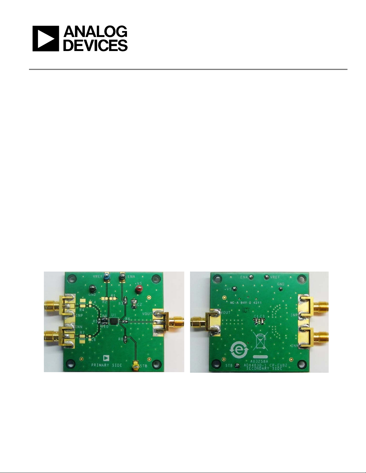
Figure 1 shows the bare evaluation board, component side and
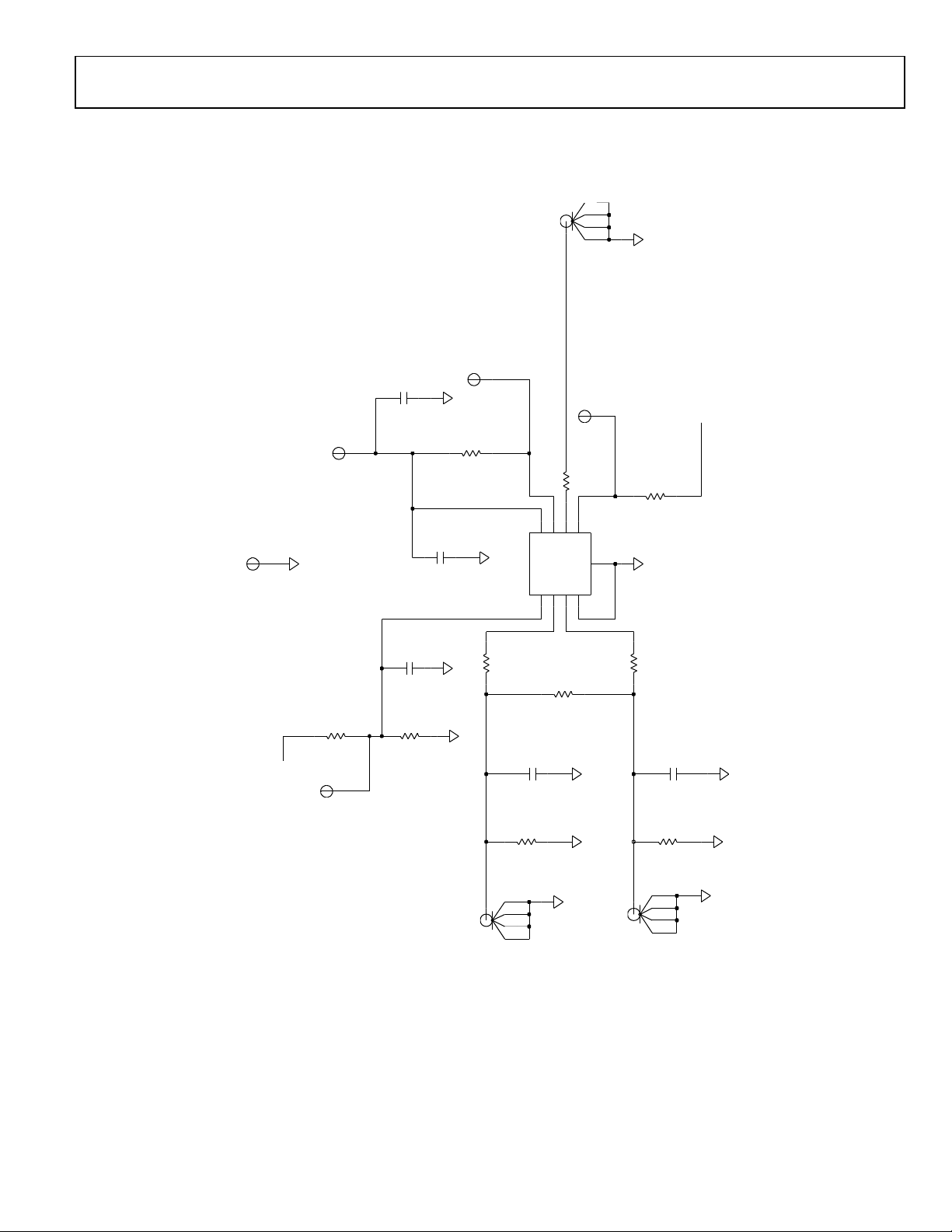
circuit side. Figure 2 shows the evaluation board schematic. The
PCB layout pattern for the PCB is shown in Figure 3 and Figure 4.
NOTES
1. THE
VALUATION BOARD SIL K SCRE E N PART NUMBER LA BELING ON Y O UR BO AR D MAY BE DIFF E R ENT
FROM WHAT IS SHOWN HERE.
Figure 1. ADA4830-1BCP-EBZ Component Side (Primary) and Circuit Side (Secondary) of PCB
PLEASE SEE THE LAST PAGE FOR AN IMPORTANT
WARNING AND LEGAL TERMS AND CONDITIONS.
DIGITAL PICTURE OF EVALUATION BOARD
Rev. 0 | Page 1 of 8
SECONDARY SIDEPRIMARY SIDE
10543-001

UG-377 Evaluation Board User Guide
TABLE OF CONTENTS
Features .............................................................................................. 1
General Description ......................................................................... 1
Digital Picture of Evaluation Board ............................................... 1
Revision History ............................................................................... 2
REVISION HISTORY
2/12—Revision 0: Initial Version
Evaluation Board Schematic and Artwork .....................................3
Ordering Information .......................................................................5
Bill of Materials ..............................................................................5
Rev. 0 | Page 2 of 8

Evaluation Board User Guide UG-377
10543-002
R7
R4
C2
R3
R8
R6
5 4 3 2
1
VOUT
1
ENA
1
STB
1
GND
1
+VS1
VREF
R1
5432
1
INN
5432
1
INP
R2
R9
R10
R5
C6
C4
C1
C3
4
1
685
PAD
2
3
7
U1
TBD1210
DNI
DNI
+VS
JOHNSON142-0701-851
TBD0603
TBD0805
JOHNSON142-0701-851
ADA4830-1
0
GRN
+VS
DNI
YEL
75
+VS
4.75K
BLK
0.1UF
4.7UFTBD0805
DNI
75
0
TBD0603
BLU
RED
TBD0805
DNI
DNI
TBD1210
JOHNSON142-0701-851
DNI
10UF
PAD
VDD
ENA
VOUT
STBVSS
INN
INP
VREF
EVALUATION BOARD SCHEMATIC AND ARTWORK
Figure 2. ADA4830-1BCP-EBZ Board
Rev. 0 | Page 3 of 8

UG-377 Evaluation Board User Guide
10543-003
10543-004
Figure 3. ADA4830-1BCP-EBZ Board Layout Pattern, Primary Side
Figure 4. ADA4830-1BCP-EBZ Board Layout Pattern, Secondary Side
Rev. 0 | Page 4 of 8

Evaluation Board User Guide UG-377
2
R5, R6
75 Ω resistor
0603
ORDERING INFORMATION
BILL OF MATERIALS
Table 1.
Quantity Reference Designator Description Package
1 U1 ADA4830-1 8-lead LFCSP
1 +V
1 C1 0.1 µF chip capacitor 0805
1 C2 10 µF chip capacitor 1210
1 C3 4.7 µF chip capacitor 0805
1 ENA Green test point loop connector TP1
1 GND Black test point loop connector TP1
3 INN, INP, VOUT SMA coaxial end launch connector
2 R9, R10 0 Ω resistor 0603
1 R8 4.99 kΩ resistor 0603
1 STB Yellow test point loop connector TP1
1 VREF Blue test point loop connector TP1
3 R1, R2, R3 Do not install resistors 0805
2 C4, C6 Do not install capacitors 0603
2 R4, R7 Do not install resistors 1210
S
Red test point loop connector TP1
Rev. 0 | Page 5 of 8

UG-377 Evaluation Board User Guide
NOTES
Rev. 0 | Page 6 of 8

Evaluation Board User Guide UG-377
NOTES
Rev. 0 | Page 7 of 8

UG-377 Evaluation Board User Guide
LY. Customer understands and agrees that the Evaluation Board is provided
SORS BE LIABLE FOR ANY INCIDENTAL, SPECIAL, INDIRECT, OR CONSEQUENTIAL DAMAGES RESULTING FROM CUSTOMER’S POSSESSION OR USE OF
in accordance with the substantive laws of the Commonwealth of
NOTES
ESD Caution
ESD (electrostatic discharge) sensitive device. Charged devices and circuit boards can discharge without detection. Although this product features patented or proprietary protection
circuitry, damage may occur on devices subjected to high e nergy ESD. Therefore, proper ES D precautions should be taken t o avoid performance degradation or loss of functionality.
Legal Terms and Conditions
By using the evaluation board discussed herein (together with any tools, components documentation or support materials, the “Evaluation Board”), you are agreeing to be bound by the terms and conditions
set forth below (“Agreement”) unless you have purchased the Evaluation Board, in which case the Analog Devices Standard Terms and Conditions of Sale shall govern. Do not u se the Evaluation Board until you
have read and agreed to the Agreement. Your use of the Evaluation Board shall signify your acceptance of the Agreement. This Agreement is made by and between you (“Customer”) and Analog Devices, Inc.
(“ADI”), with its principal place of business at One Technology Way, Norwood, MA 02062, USA. S ubject to the terms and conditions of the Agreement, ADI hereby grants to Customer a free, limited, personal,
temporary, non-exclusive, non-sublicensable, non-transferable license to use the Evaluation Board FOR EVALUATION PURPOSES ON
for the sole and exclusive purpose referenced above, and agrees not to use the Evaluation Board for any other purpose. Furthermore, the license granted is expressly made subjec t to the following additional
limitations: Customer shall not (i) rent, lease, display, sell, transfer, assign, sublicense, or distribute the Evaluation Board; and (ii) permit any Third Party to access the Evaluation Board. As used herein, the term
“Third Party” includes any entity other than ADI, Customer, their employees, affiliates and in-house consultants. The Evaluation Board is NOT sold to Customer; all rights not expressly granted herein, including
ownership of t he Evaluation Board, are res erved by ADI. CONFIDENTIA LITY. This Agreement and t he Evaluation Board shall all be considered the confidential a nd proprietary information o f ADI. Customer may
not disclose or transfer any portion of the Evaluation Board to any other party for any reason. Upon discontinuation of use of the Evaluation Board or termination of this Agreement, Customer agrees to
promptly return the Evaluation Board to ADI. ADDITIONAL RESTRICTIONS. Customer may not disassemble, decompile or reverse engineer chips on the Evaluation Board. Customer shall inform ADI of any
occurred damages or any modifications or alterations it makes to the Evaluation Board, including but not limited to soldering or any other activity that affects the material content of the Evaluation Board.
Modifications to the Evaluation Board mu st comply with applicable law, including but not limited to the RoHS Directi ve. TERMINATION. ADI may terminate this Agreement at any time upon giving written notice
to Customer. Customer agrees to return to ADI the Evaluation Board at that time. LIMITATION OF LIABILITY. THE EVALUATION BOARD PROVIDED HEREUNDER IS PROVIDED “AS IS” AND ADI MAKES NO
WARRANTIES OR REP RESENTATIONS OF ANY KIND WITH RESP ECT TO IT. ADI SPECIFICA LLY DIS CLAIMS ANY REPRESENTATIONS, ENDORSE MENTS, GUARANTEES, OR WARRANTIES, EXPRESS OR IMPLIED, RELATED
TO THE EVALUATION BOARD INCLUDING, BUT NOT LIMITED TO, THE IMPLIED WARRANTY OF MERCHANTABILITY, TITLE, FITNESS FOR A PARTICULAR PURPOSE OR NONINFRINGEMENT OF INTELLECTUAL
PROPERTY RIGHTS. IN NO EVENT WILL ADI AND ITS LICEN
THE EVALUATION BOARD, INCLUDING BUT NOT LIMITED TO LOST PROFITS, D ELAY COSTS, LAB OR COSTS OR LOSS OF GOODWILL. ADI’S TOTAL LIABILIT Y FROM ANY AND ALL CAUSES SHALL BE LIMITED TO THE
AMOUNT OF ONE HUNDRED US DOLLARS ($100.00). EXPORT. Customer agrees that it will not directly or indirectly export the Evaluation Board to another country, and that it will comply with all applicable
United States federal laws and regulations relating to exports. GOVERNING LAW. This Agreement shall be governed by and construed
Massachusetts (excluding conflict of law rules). Any legal action regarding this Agreement will be heard in t he state or federal courts having jurisdiction in Suffolk County, Massachusetts, and Customer hereby
submits to the personal jurisdiction and venue of such courts. The United Nations Convention on Contracts for the Internation al Sale of Goods shall not apply to this Agreement an d is expressly disclai med.
©2012 Analog Devices, Inc. All rights reserved. Trademarks and
registered trademarks are the property of their respective owners.
UG10543-0-2/12(0)
Rev. 0 | Page 8 of 8
 Loading...