Evaluation Board User Guide
UG-323
10201-001
One Technology Way • P. O. Box 9106 • Norwood, MA 02062-9106, U.S.A. • Tel: 781.329.4700 • Fax: 781.461.3113 www.analog.com
Evaluation Board for the AD5111 Digital Potentiometer
FEATURES
Full-featured evaluation board for the AD5111
Several test circuits
Various ac/dc input signals
PC control via a separately purchased system demonstration
platform (SDP)
PC control software
PACKAGE CONTENTS
EVAL-AD511xSDZ evaluation board
CD that includes
Self-installing software that allows users to control the
board and exercise all functions of the device
Electronic version of the AD5111 data sheet
Electronic version of the UG-323 user guide
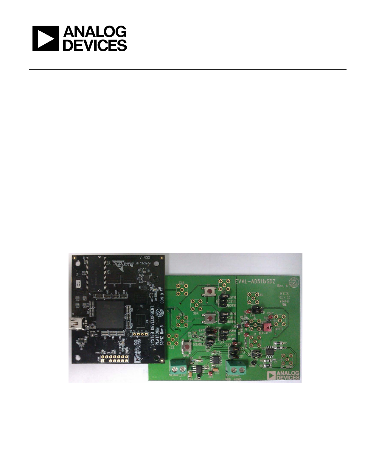
DIGITAL PICTURE OF EVALUATION BOARD WITH SYSTEM DEMONSTRATION PLATFORM
GENERAL DESCRIPTION
This user guide describes the evaluation board for evaluating the
AD5111—a single-channel, 128-position, nonvolatile memory
digital potentiometer.
The AD5111 supports single-supply 2.3 V to 5.5 V operation,
making the device suited for battery-powered applications and
many other applications, offering guaranteed low resistor
tolerance errors of ±8% and high bandwidth while allowing up
to ±6 mA current density in the A, B, and W pins.
A simple 3-wire up/down interface allows manual switching or
high speed digital control with clock rates up to 50 MHz.
T h e EVA L-AD5111SDZ can operate in single-supply mode and
incorporates an internal power supply from the USB.
Complete specifications for the AD5111 part can be found in
the AD5111 data sheet, which is available from Analog Devices,
Inc., and should be consulted in conjunction with this user
guide when using the evaluation board.
PLEASE SEE THE LAST PAGE FOR AN IMPORTANT
WARNING AND LEGAL TERMS AND CONDITIONS.
Figure 1.
Rev. 0 | Page 1 of 12

UG-323 Evaluation Board User Guide
TABLE OF CONTENTS
Features .............................................................................................. 1
Package Contents .............................................................................. 1
General Description ......................................................................... 1
Digital Picture of Evaluation Board with System Demonstration
Platform ............................................................................................. 1
Revision History ............................................................................... 2
Evaluation Board Hardware ............................................................ 3
Power Supplies .............................................................................. 3
Link Options ................................................................................. 3
REVISION HISTORY
11/11—Revision 0: Initial Version
Test Circuits ...................................................................................4
Evaluation Board Software ...............................................................5
Installing the Software ..................................................................5
Running the Software ...................................................................5
Operating the Software .................................................................6
Evaluation Board Schematics and Artwork ...................................7
Ordering Information .................................................................... 11
Bill of Materials ........................................................................... 11
Rev. 0 | Page 2 of 12

Evaluation Board User Guide UG-323
+5V (from SDP).
+3V3 (from SDP).
EVALUATION BOARD HARDWARE
POWER SUPPLIES
The EVAL-AD5111SDZ supports using single power supplies.
The evaluation board can be powered either from the SDP port
or externally by the EXTERNAL-1 and EXTERNAL-2
connectors, as described in Ta ble 2.
All supplies are decoupled to ground using 10 µF tantalum and
0.1 µF ceramic capacitors.
Table 2. Maximum and Minimum Voltages of the Connectors
Connector Number Label Voltage
EXTERNAL-1 VDD Analog positive power supply, VDD.
If connected to the SDP, it is 3.3 V to 5.5 V.
If controlled externally , it is 2.3 V to 5.5 V.
EXTERNAL-2 AGND Analog ground, AGND.
LINK OPTIONS
One link option is incorporated in the evaluation board and
should be set up before using the board. Tab le 1 describes the
position of the link to control the evaluation board by a PC, via
the SDP board, using the EVAL-AD5111SDZ. The functions of
this link option is described in detail in Tab le 3.
Table 1. Link Options Setup for SDP Control (Default)
Link No. Option
LK8 +5V
Table 3. Link Functions
Link Number Power Supply Options
LK8 VDD This link selects one of the following as the positive power supply:
EXT1 (external supply from the EXTERNAL-1 connector).
1
If the part is powered using the external connector without connecting the SDP board, +5V jumper must be connected as well.
Rev. 0 | Page 3 of 12

UG-323 Evaluation Board User Guide
10201-002
BUF-W
750Ω
12Ω
V
DD
VOUT
AC
DC
GND
AC
R9
W
A
B
A
W
B
R8
V
DD
2
V
DD
2
256
)(
RDAC
VVV
B
A
OUT
×−=
10201-003
BUF-W
750Ω
f
C
= 200Hz
12Ω
VOUT
AC
AC_INPUT
GND
AC
R9
R7
W
A
B
A
W
B
R8
V
DD
2
V
DD
2
HPF
×≈
128
log20)dB(
RDAC
nAttenuatio
TEST CIRCUITS
The E VA L -AD5111SDZ incorporates several test circuits to
evaluate the AD5111 performance.
DAC
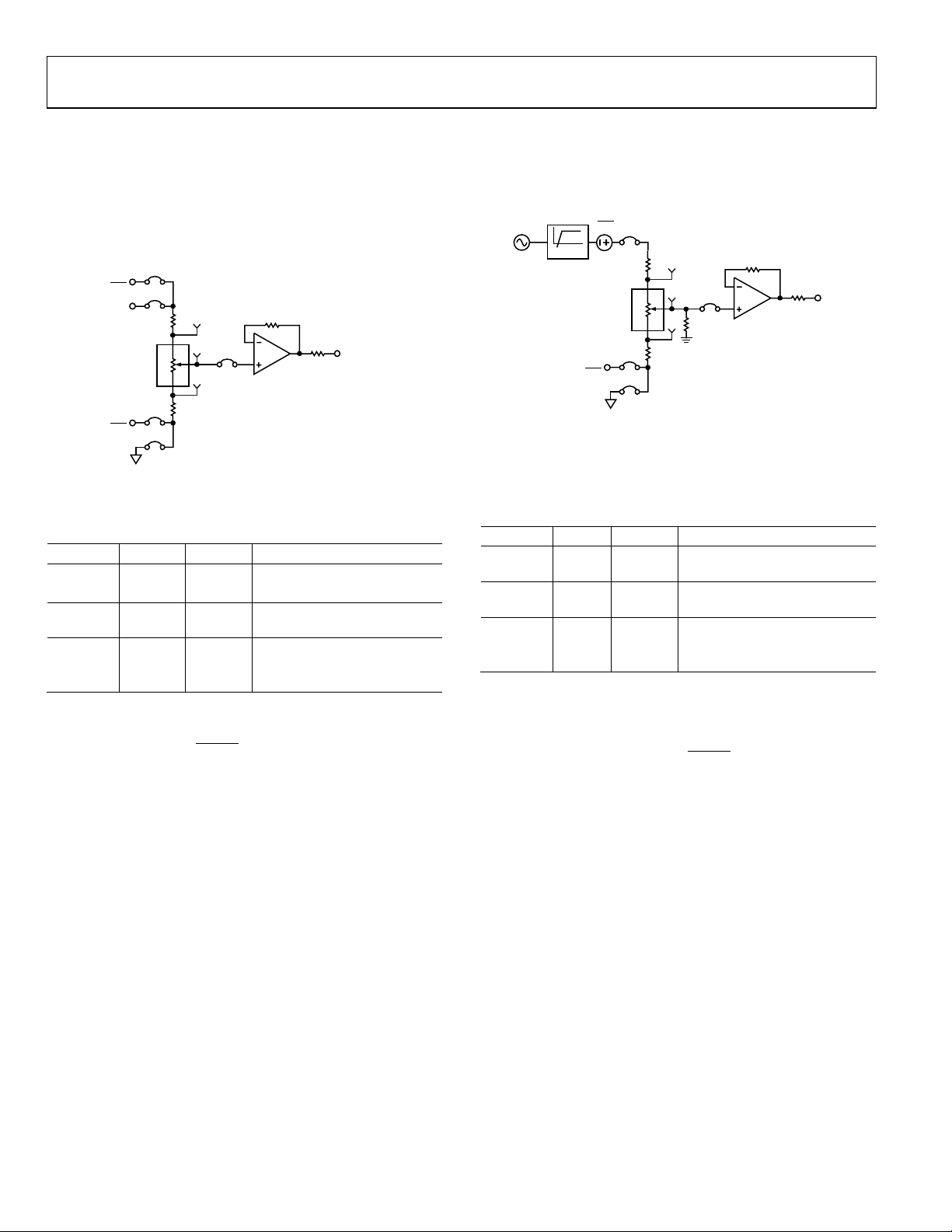
The AD5111 can be operated as a digital-to-analog converter
(DAC), as shown in Figure 2.
AC Signal Attenuation
The AD5111 can be used to attenuate an ac signal, which must
be provided externally using the AC_INPUT connector, as
shown in Figure 3.
Figure 2. DAC
Table 4 shows the options available for the voltage references.
Table 4. DAC Voltage References
Term inal Link Options Description
A LK1 AC Connects Terminal A to VDD/2
DC Connects Terminal A to VDD
W BUF-W Connects Terminal W to an
output buffer
B LK6 AC Connects Terminal B to VDD/2
GND Connects Terminal B to
analog ground
The output voltage is defined in Equation 1.
(1)
where:
RDAC is the code loaded in the RDAC register.
V
is the voltage applied to Terminal A (LK1 link).
A
V
is the voltage applied to Terminal B (LK6 link)
B
However, by using the R8 and R9 external resistors, the user can
reduce the voltage of the voltage references. In this case, use the
A and B test points to measure the voltage applied to the A and
B terminals and recalculate V
and VB in Equation 1.
A
Figure 3. AC Signal Attenuator
Depending on the voltage supply rails and the dc offset voltage
of the ac signal, various configurations can be used as described
in Table 5.
Table 5. AC Signal Attenuation Link Options
Term inal Link Options Description
A LK1 AC Remove dc voltage and biased
the signal to V
/2
DD
W BUF-W Connects Terminal W to an
output buffer
B LK6 AC1 Connects Terminal B to VDD/2
GND Connects Terminal B to analog
ground
1
Recommended to ensure optimal total harmonic distortion (THD) performance.
The signal attenuation is defined in Equation 2.
(2)
where:
RDAC is the code loaded in the RDAC register.
In addition, R7 can be used to achieve an exponential attenuation. To do so, adjust the R7 resistor until a desirable transfer
function is found, typically around 1.6 kΩ for a 10 kΩ
potentiometer.
Rev. 0 | Page 4 of 12

Evaluation Board User Guide UG-323
10201-004
10201-005
EVALUATION BOARD SOFTWARE
INSTALLING THE SOFTWARE
The EVAL-AD5111SDZ evaluation kit includes evaluation
board software provided on a CD. The software is compatible
with Windows® XP, Windows Vista, and Windows 7 (both 32
and 64 bits).
Install the software before connecting the SDP board to the USB
port of the PC to ensure that the SDP board is recognized when
it is connected to the PC.
1. Start the Windows operating system and insert the CD.
2. The installation software opens automatically. If it does
not, run the setup.exe file from the CD.
3. After the installation is completed, power up the evaluation
board as described in the Power Supplies section.
4. Plug t he EVAL -AD511xSDZ into the SDP board and the SDP
board into the PC using the USB cable included in the box.
5. When the software detects the evaluation board, follow the
instructions that appear to finalize the installation.
To uninstall the program, click Start > Control Panel > Add or
Remove Programs > AD5111 Eval Board.
RUNNING THE SOFTWARE
To run t h e evaluation board software, do the following:
1. Click Start > All Programs > Analog Devices > AD5111 >
AD5111 Eval Board.
2. If the SDP board is not connected to the USB port when
the software is launched, a connectivity error is displayed
(see Figure 4). Connect the evaluation board to the USB
port of the PC, wait a few seconds, click Rescan, and follow
the instructions.
Figure 4. Pop-Up Window Error
The main window of the EVA L-AD5111SDZ evaluation
software then opens, as shown in Figure 5.
Figure 5. EVAL-AD5111SDZ Evaluation Board Software Main Window
Rev. 0 | Page 5 of 12

UG-323 Evaluation Board User Guide
OPERATING THE SOFTWARE
The main window of the EVA L-ADAD5111SDZ software is
divided into five different operations: INCREMENT,
DECREMENT, SHUTDOWN, STORE, and EXIT. The
operations are as follows:
• The INCREMENT button increases the RDAC value by
the number of steps selected by the window.
• The DECREMENT button decreases the RDAC value by
the number of steps selected by the window.
• The SHUTDOWN button places the part in shutdown.
• The STORE button stores the data contained in the RDAC
register to the memory.
• Clicking EXIT closes the program but does not reset the part.
Rev. 0 | Page 6 of 12

Evaluation Board User Guide UG-323
10201-006
EVALUATION BOARD SCHEMATICS AND ARTWORK
Figure 6. Schematic of the AD5111 Circuitry
Rev. 0 | Page 7 of 12

UG-323 Evaluation Board User Guide
10201-007
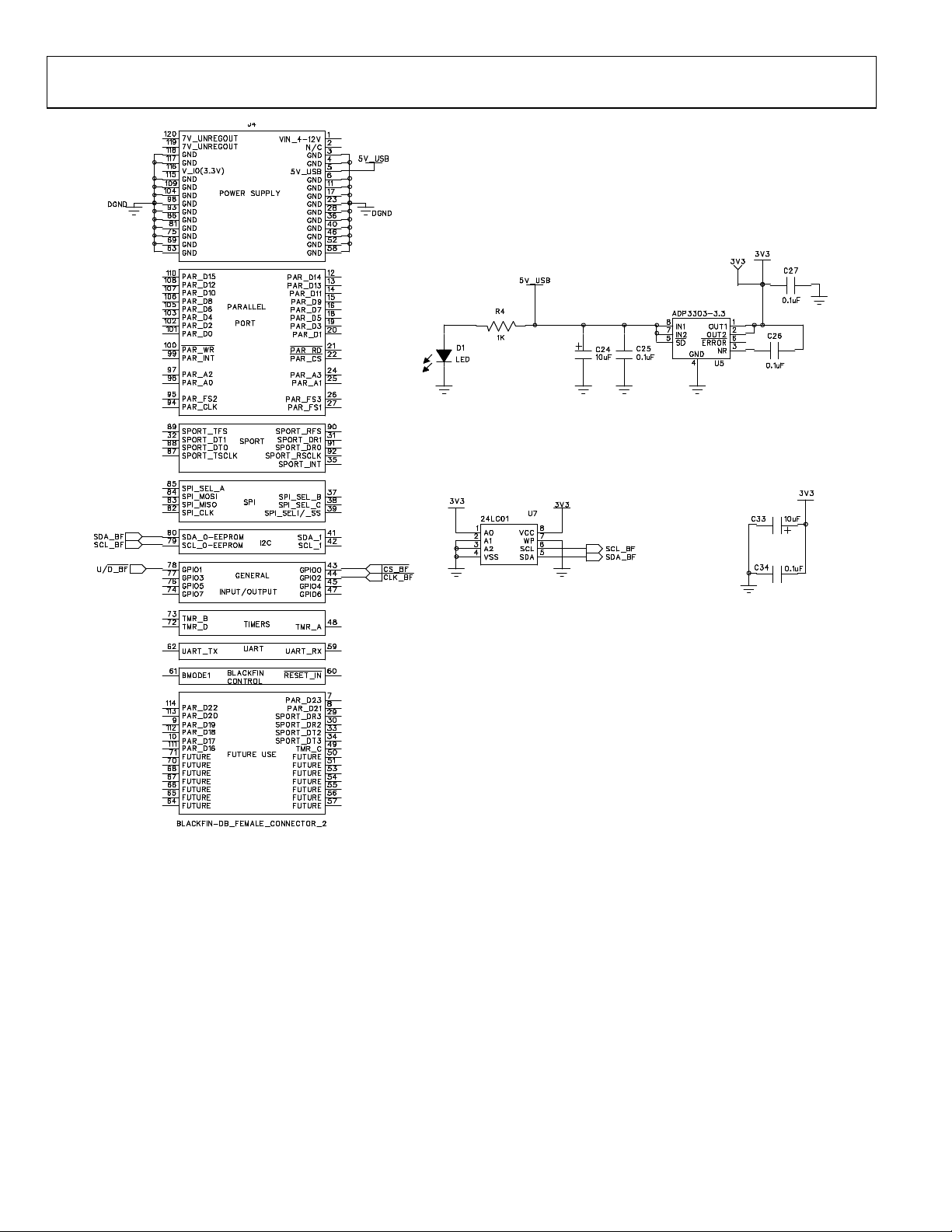
Figure 7. Schematic of SDP Connector
Rev. 0 | Page 8 of 12

Evaluation Board User Guide UG-323
10201-008
10201-009
Figure 8. Component Placement Drawing
Figure 9. Component Side PCB Drawing
Rev. 0 | Page 9 of 12

UG-323 Evaluation Board User Guide
10201-010
Figure 10. Solder Side PCB Drawing
Rev. 0 | Page 10 of 12

Evaluation Board User Guide UG-323
6
3V3, A, B, VDD, VOUT, W
Test point, PCB, red, PK100
FEC 873-1144
ORDERING INFORMATION
BILL OF MATERIALS
Table 6.
Qty Reference Designator Description Supplier1/Part Number
1 C3 100 nF, 0402 capacitor FEC 1414580
1 C1 0.1 µF, 0603 capacitor FEC 138-2224
3 C25, C26, C271 0.1 µF, 0603 capacitor FEC 301-9482
1 C24 10 µF, 1206 capacitor FEC 197-130
1 D1 Green LED FEC 579-0852
1 EXTERNAL 2-pin connector FEC 151789
1 J4 Receptacle, 0.6 mm, 120 way Digi-Key H1219-ND
6 LK1, LK3, LK4, LK5, LK6, LK8 Header, 2-row, 36 + 36 way, and jumper socket, black FEC 148-535 and FEC 150-411
1 BUF-W Header, 1-row, 2-way, and jumper socket, black FEC 102-2247 and FEC 150-411
1 R11 12 Ω, 0603, 1% resistor FEC 9330534
1 R10 750 Ω, 0603, 1% resistor FEC 9331506
1 R4 1 kΩ, 0603, 0.01% resistor FEC 9330380
4 R5, R6, R12, R13 2.7 kΩ, 1206, 1% resistor FEC 9337288
2 R8, R9 0 Ω, 0603 resistor FEC 9331662
2 DGND, AGND Test point, PCB, black, PK100 FEC 873-1128
1 U1 AD5111 Analog Devices AD5111
1 U3 ADA4860 Analog Devices ADA4860
1 U5 ADP3303 Analog Devices ADP3303
1 U7 24LC64 serial EEPROM FEC 9758070
1 U15 AD8652 Analog Devices AD8652
1
FEC refers to Farnell Electronic Component Distributors.
Rev. 0 | Page 11 of 12

UG-323 Evaluation Board User Guide
TERMINATION. ADI may terminate this Agreement at any time upon giving written notice
ED WARRANTY OF MERCHANTABILITY, TITLE, FITNESS FOR A PARTICULAR PURPOSE OR NONINFRINGEMENT OF INTELLECTUAL
governed by and construed in accordance with the substantive laws of the Commonwealth of
NOTES
I2C refers to a communications protocol originally developed by Philips Semiconductors (now NXP Semiconductors).
ESD Caution
ESD (electrostatic discharge) sensitive device. Charged devices and circuit boards can discharge without detection. Although this product features patented or proprietary protection
circuitry, damage may occur on devices subjected to high e nergy ESD. Therefore, proper ESD precaution s should be taken to avoid per forma nce degra dation or loss of functionality.
Legal Terms and Conditions
By usin g the evaluation board discussed herein (together with any tools, components documentation or support materials, the “Evaluation Board”), you are agreeing to be bound by the terms and conditions
set forth below (“Agreement”) unless you have purchased the Evaluation Board, in w hich case the Analog Devices Standard Te rms and Conditions of Sale shall govern. Do not use the Evaluation Board until you
have read and agreed to the Agreement. Your use of the Evaluation Board shall signify your acceptance of the Agreement. This Agreement is made by and between you (“Customer”) and An alog Devices, Inc.
(“ADI”), with its principal place of business at One Technology Way, Norwood, MA 02062, USA. S ubject to the terms and conditions of the Agreement, ADI hereby grants to Customer a free, limited, personal,
temporary, non-exclusive, non-sublicensable, non-transferable license to use the Evaluation Board FOR EVALUATION PURPOSES ONLY. Customer understands and agrees that the Evaluation Board is provided
for the sole and exclusive purpose referenced above, and agrees not to use the Evaluation Board for any other purpose. Furthermore, the license granted is expressly made subject to the following additional
limitations: Customer shall not (i) rent, lease, display, sell, transfer, assign, sublicense, or distribute the Evaluation Board; and (ii) permit any Third Party to access the Evaluation Board. As used herein, the term
“Third Party” includes any entity other than ADI, Customer, their employees, affiliates and in-house consultants. The Evaluation Board is NOT sold to Customer; all rights not expressly granted herein, including
ownership of the Evaluation Board, are reserved by ADI. CONFIDENTIALIT Y. This Agreement and the Evaluation Board shall all be considered the confidential and proprietary information of A DI. Custom er may
not disclose or transfer any portion of the Evaluation Board to any other party for any reason. Upon discontinuation of use of the Evaluation Board or termination of this Agreement, Customer agrees to
promptl y return the Evaluation Board to ADI. ADDITIONAL RESTRICTIONS. Customer may not disassemble, decompile or reverse engineer chips on the Evaluation Board. Customer shall inform ADI of any
occurred damages or any modifications or alterations it makes to the Evaluation Board, including but not limited to soldering or any other activity that affects the material content of the Evaluation Board.
Modifications to the Evaluation Board must comply with applicable law, including but not limited to the RoHS Directive.
to Customer. Customer agrees to return to ADI the Evaluation Board at that time. LIMITATION OF LIABILITY. THE EVALUATION BOARD PROVIDED HEREUNDER IS PROVIDED “AS IS” AND ADI MAKES N O
WARRANTIES OR REPRES ENTATIONS OF ANY KIND WITH RESPECT TO IT. ADI SPECIFICAL LY DISC LAIMS ANY REPRESENTATIONS, ENDORSEMENTS, GUA RANTEES, OR WARRANT IES, EXPRESS OR IMPLIED, RELATED
TO THE EVALUATION BOARD INCLUDING, BUT NOT LIMITED TO, THE IMPLI
PROPERTY RIGHTS. IN NO EVENT WILL ADI AND ITS LICENSORS BE LIABLE FOR ANY INCIDENTAL, SPECIAL, INDIRECT, OR CONSEQUENTIAL DAMAGES RESULTING FROM CUSTOMER’S POSSESSION OR USE OF
THE EVALUAT ION BOARD, INCLUDING BUT NOT LIMI TED TO LOST PROFITS, DE LAY COSTS, LABOR COSTS OR LOSS OF GOODWI LL. ADI’S TOTAL LIA BILITY FROM AN Y AND ALL CAUSES S HALL BE LIMITE D TO THE
AMOUNT OF ONE HUNDRED US DOLLARS ($100.00). EXPORT. Customer agrees that it will not directly or indirectly export the Evaluation Board to another country, and that it will comply with all applicable
United States federal laws and regulations relating to exports. GOVERNING LAW. This Agreement shall be
Massachusetts (excluding conflict of law rules). Any legal action regarding this Ag re ement will be heard in the state or federal courts having juri sdic tion in Suffolk County, Massachusetts, and Customer hereby
submits to the personal jurisdiction and venue of such courts. The United Nations Convention on Contracts for the International Sale of Goods shall no t apply to this Agreement and is exp ressly disclaimed.
©2011 Analog Devices, Inc. All rights reserved. Trademarks and
registered trademarks are the property of their respective owners.
UG10201-0-11/11(0)
Rev. 0 | Page 12 of 12
 Loading...