

Evaluation Board User Guide
One Technology Way • P. O . Box 9106 • Norwood, MA 02062-9106, U.S.A. • Tel : 781.329.4700 • Fax : 781.461.3113 • www.analog.com
UG-219
Evaluating the ADP2370/ADP2371 Buck Regulators
FEATURES
Buck regulator input voltage range: 3.2 V to 15 V
Buck regulator output current: 800 mA
Operating temperature range: −40°C to +125°C
EQUIPMENT NEEDED
Voltage meters, current meters, power supply
Resistive or electronic loads
DOCUMENTS NEEDED
ADP2370/ADP2371 data sheet
UG-220 user guide
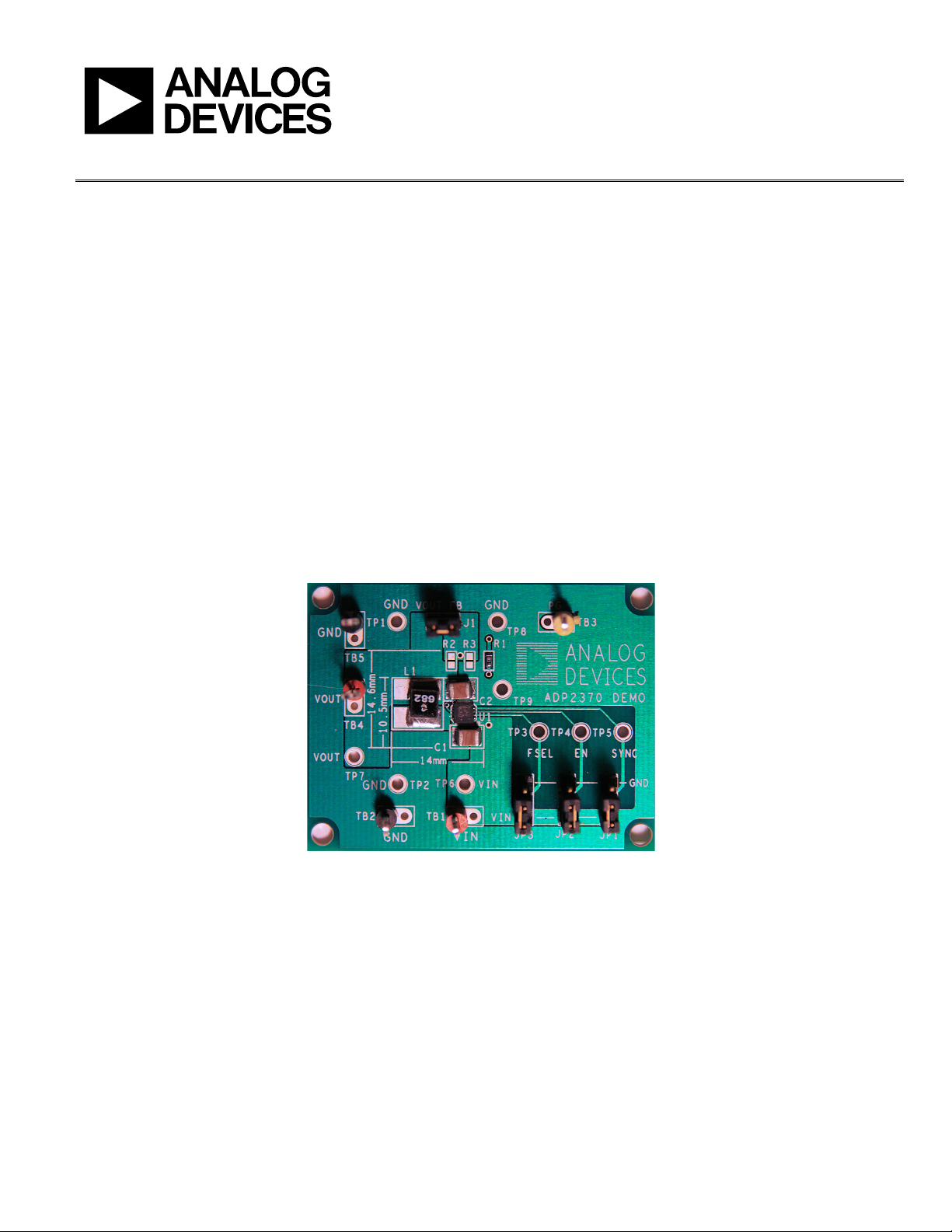
DIGITAL PICTURE OF THE EVALUATION BOARD
GENERAL DESCRIPTION
The ADP2370/ADP2371 evaluation boards (ADP2370CP-EVALZ
and ADP2371CP-EVALZ) are used to demonstrate the functionality of the ADP2370/ADP2371 buck regulators.
Basic electrical performance measurements, such as line and load
regulation, efficiency, and ground current, can be demonstrated
with a few voltage supplies, voltage meters, current meters, and
load resistors.
Complete information about the ADP2370/ADP2371 buck regulators is available in the ADP2370/ADP2371 data sheet, which
should be consulted in conjunction with this user guide when
using the evaluation board.
PLEASE SEE THE LAST PAGE FOR AN IMPORTANT
WARNING AND LEGAL TERMS AND CONDITIONS.
Figure 1.
Rev. 0 | Page 1 of 12
09532-001

UG-219 Evaluation Board User Guide
TABLE OF CONTENTS
Features .............................................................................................. 1
Equipment Needed ........................................................................... 1
Documents Needed .......................................................................... 1
General Description ......................................................................... 1
Digital Picture of the Evaluation Board ......................................... 1
Revision History ............................................................................... 2
Evaluation Board Hardware and Schematic ................................. 3
Evaluation Board Configuration ................................................ 3
Output Voltage Accuracy Measurements ...................................... 4
REVISION HISTORY
4/12—Revision 0: Initial Version
Line Regulation Measurements ...................................................5
Load Regulation Measurements ..................................................5
Efficiency Measurements .................................................................6
Calculating the Efficiency ............................................................7
Quiescent Current Measurements ..................................................8
Quiescent Current Consumption ...............................................9
Ordering Information .................................................................... 10
Bill of Materials ........................................................................... 10
Related Links ............................................................................... 10
Rev. 0 | Page 2 of 12
Evaluation Board User Guide UG-219
ADJ only (5V )
ADJ only (5V )
PG
SW
VOUT
VIN
FSEL
EN
SYNC
VOUT
TB4
U1
ADP2370/ADP2371
VIN
1
FSEL
2
EN
3
PG
6
SW
7
PGND
8
SYNC
4
FB
5
TP4
1
TP9
1
JP2
EN
1
1
2
2
3
3
TP5
1
GND
TB2
R1
10K
TP6
1
JP3
Freq
1
1
2
2
3
3
TP7
1
R2
422K
JP1
Sync
1
1
2
2
3
3
TP1
1
C2
10UF
VIN
TB1
PG
TB3
GND
TB5
R3
80.6K
TP2
1
L1
6.8uH
J1
1 2
TP8
1
C1
10UF
TP3
1
09532-002
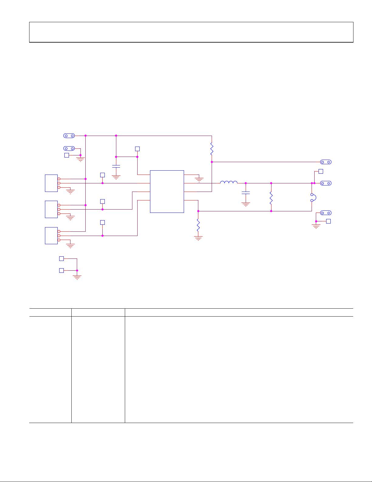
R1
Pull-up resistor
10 kΩ pull-up resistor for power good (PG).
EVALUATION BOARD HARDWARE AND SCHEMATIC
EVALUATION BOARD CONFIGURATION
The ADP2370/ADP2371 evaluation boards ship with all the
components necessary to perform basic electrical performance
measurements, including the input and output capacitors, buck
inductor, and power-good pull-up resistor. The placement of
the critical components for the buck regulator (inductor and
capacitors) has been optimized for low noise and the smallest
possible footprint.
Figure 2 shows the schematic of the evaluation board configuration. Tab le 1 describes the hardware components.
For complete information about the ADP2370/ADP2371 buck
regulators, see the ADP2370/ADP2371 data sheet.
Figure 2. Evaluation Board Schematic
Table 1. Evaluation Board Hardware Components
Component Function Description
U11 Buck regulator ADP2370 or ADP2371 buck regulator.
C1 Input capacitor 10 μF input bypass capacitor required for transient performance.
C2 Output capacitor 10 μF output capacitor required for stability and transient performance.
L12 Inductor 6.8 μH inductor for 3.3 V output at 1.2 MHz.
R2 Resistor 422 kΩ, 1% resistor. With R3, sets the output voltage to 5 V (adjustable version only).
R3 Resistor 80.6 kΩ, 1% resistor. With R2, sets the output voltage to 5 V (adjustable version only).
JP1 Jumper When JP1 is connected to VIN, forced PWM mode is enabled. When JP1 is connected to GND,
JP2 Jumper When JP2 is connected to VIN, the output is enabled. When JP2 is connected to GND, the output
JP3 Jumper When JP3 is connected to VIN, 1.2 MHz operation is selected. When JP3 is connected to GND,
J1 Jumper Connects the FB pin to the buck regulator output (fixed output version only).
1
Component varies depending on the evaluation board model ordered.
2
Inductor value varies depending on the output voltage.
auto mode is enabled. When JP1 is connected to SYNC, an external clock can be used to set the
operating frequency.
is disabled.
600 kHz operation is selected.
Rev. 0 | Page 3 of 12

UG-219 Evaluation Board User Guide
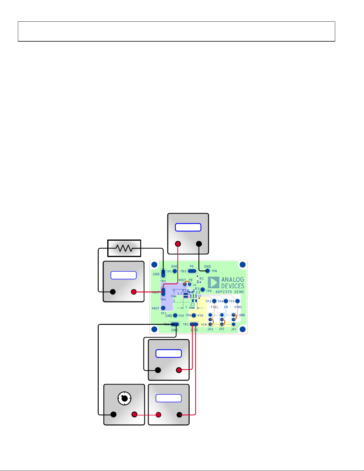
OUTPUT VOLTAGE ACCURACY MEASUREMENTS
Figure 3 shows how to connect the evaluation board to a voltage
source and a voltage meter (voltmeter) for basic output voltage
accuracy measurements. A resistor can be used as the load for the
buck regulator. Ensure that the resistor has a power rating adequate
to handle the power that is expected to be dissipated across it. An
electronic load can be used as an alternative. In addition, ensure
that the voltage source can supply enough current for the expected
load levels.
Follow these steps to connect the evaluation board to a voltage
source and voltage meter:
1. Connect the negative terminal (−) of the voltage source
to the GND pad (TB2) on the evaluation board.
2. Connect the positive terminal (+) of the voltage source
to the VIN pad (TB1) on the evaluation board.
3. Connect a load between the VOUT pad (TB4) and one
of the GND pads on the evaluation board.
4. Connect the negative terminal (−) of the voltmeter to one
of the GND pads on the evaluation board.
5. Connect the positive terminal (+) of the voltmeter to the
VOUT pad (TP7) on the evaluation board.
6. Connect a jumper between Pin 1 and Pin 2 of JP2 to enable
the buck regulator.
7. Connect a jumper between Pin 3 and Pin 2 of JP1 to enable
auto mode.
8. Connect a jumper between Pin 1 and Pin 2 of JP3 to enable
1.2 MHz operation.
9. Turn on the voltage source.
If the load current is large, connect the voltage meter as close to
TB4 as possible to reduce the effects of IR drops.
LOAD
VOLTMETER
1.99711
–
+
VOLTAGE SOURCE
–
Figure 3. Buck Regulator Output Voltage Regulation Measurement Setup
Rev. 0 | Page 4 of 12
+
09532-004

Evaluation Board User Guide UG-219
3.10
3.15
3.20
3.25
3.30
3.35
3.40
3 5 7 9 11 13 15
OUTPUT VOLTAGE (V)
INPUT VOLTAGE (V)
I
LOAD
= 0.1mA
I
LOAD
= 1mA
I
LOAD
= 5mA
I
LOAD
= 10mA
I
LOAD
= 50mA
I
LOAD
= 100mA
I
LOAD
= 300mA
I
LOAD
= 800mA
09532-011
3.10
3.15
3.20
3.25
3.30
3.35
3.40
0.1 1 10 100 1000
OUTPUT VOLTAGE (V)
LOAD CURRENT ( mA)
V
IN
= 3.8V
V
IN
= 4.55V
V
IN
= 6.05V
V
IN
= 7.30V
V
IN
= 10.55V
V
IN
= 12
.05V
VIN = 15.05V
09532-012
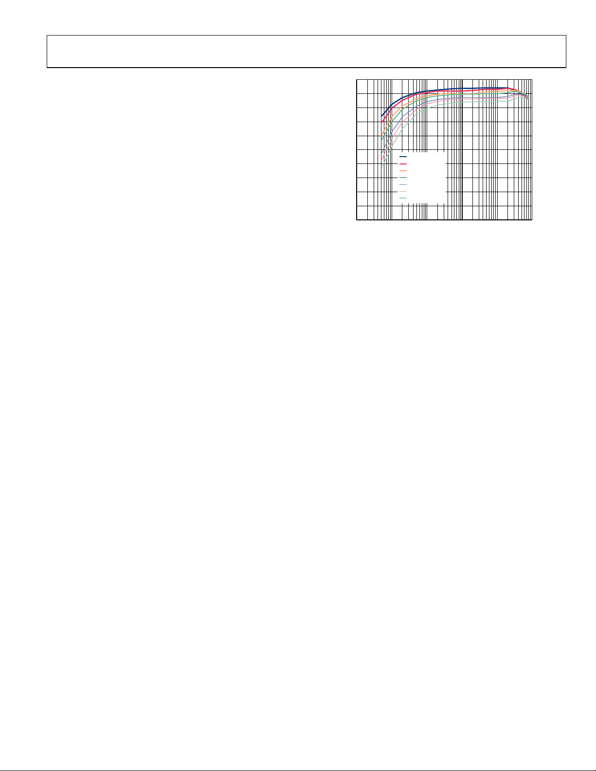
LINE REGULATION MEASUREMENTS
For line regulation measurements, the output of the buck
regulator is monitored while the input is varied. For good line
regulation, the output must change as little as possible with
varying input levels.
For example, for an ADP2370/ADP2371 with a fixed 3.3 V
output, V
can be repeated under different load conditions. Figure 4 shows
the typical line regulation performance of an ADP2370/ADP2371
with a fixed 3.3 V output.
must be varied from 3.8 V to 15 V. This measurement
IN
LOAD REGULATION MEASUREMENTS
For load regulation measurements, the output of the buck
regulator is monitored while the load is varied. For good load
regulation, the output must change as little as possible with
varying loads.
The input voltage must be held constant during this measurement. The load current can be varied from 0 mA to 800 mA.
Figure 5 shows the typical load regulation performance of an
ADP2370/ADP2371 with a fixed 3.3 V output for various input
voltages.
Figure 4. Output Voltage (V
) vs. Input Voltage (VIN)
OUT
Figure 5. Output Voltage (V
) vs. Load Current (I
OUT
OUT
)
Rev. 0 | Page 5 of 12
UG-219 Evaluation Board User Guide
EFFICIENCY MEASUREMENTS
Figure 6 shows how to connect the evaluation board to a voltage
source, two voltage meters, and two current meters (ammeters)
for basic efficiency measurements. A resistor can be used as the
load for the buck regulator. Ensure that the resistor has a power
rating adequate to handle the power that is expected to be dissipated across it. An electronic load can be used as an alternative.
In addition, ensure that the voltage source can supply enough
current for the expected load levels.
Follow these steps to connect the evaluation board to a voltage
source and to the voltage and current meters:
1. Connect a jumper between Pin 1 and Pin 2 of JP2 to enable
the buck regulator.
2. Connect a jumper between Pin 3 and Pin 2 of JP1 to enable
auto mode.
3. Connect a jumper between Pin 1 and Pin 2 of JP3 to enable
1.2 MHz operation.
4. Connect the negative terminal (−) of the voltage source to
the GND pad (TB2) on the evaluation board.
5. Connect the positive terminal (+) of the voltage source to
the positive terminal (+) of the input ammeter.
6. Connect the negative terminal (−) of the input ammeter to
the VIN pad (TB1) on the evaluation board.
7. Connect the positive terminal (+) of the input voltmeter to
the VIN pad (TB1) on the evaluation board.
8. Connect the negative terminal (−) of the input voltmeter to
the GND pad (TB2) on the evaluation board.
9. Connect the positive terminal (+) of the output ammeter to
the VOUT pad (TB4) on the evaluation board.
10. Connect a load between the negative terminal (−) of the
output ammeter and the GND pad (TB5) on the evaluation
board.
11. Connect the positive terminal (+) of the output voltmeter
to the VOUT pad (TB4) on the evaluation board.
12. Connect the negative terminal (−) of the output voltmeter
to the GND pad (TP8) on the evaluation board.
13. Turn on the voltage source.
If the load current is large, connect the voltage meters as close
as possible to the VIN and VOUT pads to reduce the effects of
IR drops.
LOAD
AMMETER
0.00112
–
VOLTAGE SOURCE
+
VOLTMETER
1.99711
–
AMMETER
VOLTMETER
1.99711
+
+
–
0.00112
–
+
Figure 6. Buck Regulator Efficiency Measurement Setup
+
Rev. 0 | Page 6 of 12
–
09532-006
Evaluation Board User Guide UG-219
0
10
20
30
40
50
60
70
80
90
100
0.01 0.1 1.0 10 100 1000
EFFICIENCY (%)
LOAD CURRENT ( mA)
V
IN
=
3.80V
V
IN
=
4.55V
V
IN
=
6.05V
V
IN
=
7.30V
V
IN
=
10.55V
V
IN
=
12.05V
V
IN
=
15.05V
09532-019
CALCULATING THE EFFICIENCY
The efficiency is calculated as follows:
× I
Efficiency = 100% × (V
OUT
The efficiency of the buck regulator can be measured over several
combinations of input voltage and load current. Figure 7 shows
the efficiency of a 3.3 V output buck regulator over input voltage
and load current.
)/(VIN × IIN)
OUT
Figure 7. Efficiency vs. Input Voltage and Load Current
Rev. 0 | Page 7 of 12

UG-219 Evaluation Board User Guide
QUIESCENT CURRENT MEASUREMENTS
Figure 8 shows how to connect the evaluation board to two
voltage sources and a current meter for quiescent current
measurements.
Follow these steps to connect the evaluation board to the
voltage sources and to the current meter:
1. Connect a jumper between Pin 1 and Pin 2 of JP2 to enable
the buck regulator.
2. Connect a jumper between Pin 3 and Pin 2 of JP1 to enable
auto mode.
3. Connect a jumper between Pin 1 and Pin 2 of JP3 to enable
1.2 MHz operation.
4. Connect the positive terminal (+) of the input voltage
source to the positive terminal (+) of the ammeter.
5. Connect the negative terminal (−) of the ammeter to the
VIN pad (TB1) on the evaluation board.
VOLTAGE SOURCE
6. Connect the negative terminal (−) of the input voltage
source to the GND pad (TB2) on the evaluation board.
7. Remove R1. (R1 can remain in circuit, but it increases the
quiescent current by 10 kΩ/V
8. Connect the positive terminal (+) of the output voltage
source to the VOUT pad (TB4) on the evaluation board.
9. Connect the negative terminal (−) of the output voltage
source to the GND pad (TB5) on the evaluation board.
10. If the output voltage source has a current limit function,
set the current limit to 10 mA or less.
11. Set the output voltage source output voltage to ~500 mV
above the normal output voltage of the ADP2370/ADP2371
evaluation board.
12. Turn on the voltage source.
.)
IN
+
VOLTAGE SOURCE
Figure 8. Quiescent Current Measurement Setup
–
AMMETER
++
––
09532-008
Rev. 0 | Page 8 of 12
Evaluation Board User Guide UG-219
0
5
10
15
20
25
3 4 5 6 7 8 9 10 11 12 13 14 15 16
QUIESCENT CURRENT (µA)
INPUT VOLTAGE (V)
–40°C
–5°C
+25°C
+85°C
+125°C
09532-003
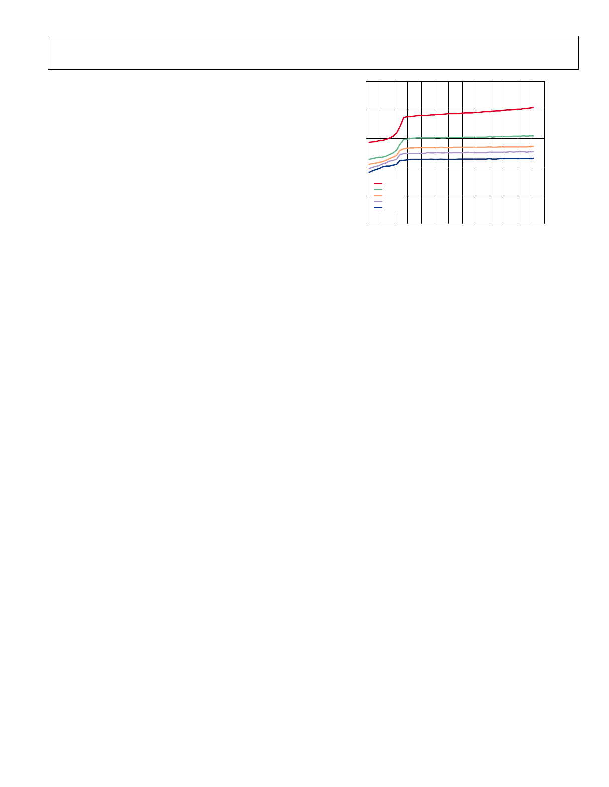
QUIESCENT CURRENT CONSUMPTION
Quiescent current measurements can determine how much
current the internal circuits of the buck regulator consume under
no load conditions. To be efficient, the regulator must consume
as little current as possible. Figure 9 shows the typical quiescent
current consumption at no load for various input voltages. When
the device is disabled (EN = PGND), quiescent current drops to
less than 2 µA.
Figure 9. Quiescent Current vs. Input Voltage, No Load
Rev. 0 | Page 9 of 12

UG-219 Evaluation Board User Guide
ORDERING INFORMATION
BILL OF MATERIALS
Table 2.
Qty Reference Designator Description Manufacturer/Vendor Vendor Part No.
2 C1, C2 Capacitor, MLCC, 10 μF, 25 V, 1210, X5R Murata or equivalent
3 JP1, JP2, JP3 Header, single, STR, three pins Digi-Key Corp. S1012E-03-ND
1 J1 Header, single, STR, two pins Digi-Key Corp. S1012E-02-ND
1 L1 Inductor, 6.8 μH, 4 mm × 4 mm × 3 mm Coilcraft XAL4030-682ME
1 R1 Resistor, 10 kΩ, 0.10 W, 0603 Vishay or equivalent
1 U1 IC, ADP2370/ADP2371 buck regulator Analog Devices, Inc. ADP2370ACPZ-3.3-R7
ADP2371ACPZ-3.3-R7
RELATED LINKS
Resource Description
ADP2370/ADP2371 Product Page
UG-220 ADP2370/ADP2371 RedyKit™ User Guide
Rev. 0 | Page 10 of 12

Evaluation Board User Guide UG-219
NOTES
Rev. 0 | Page 11 of 12

UG-219 Evaluation Board User Guide
and between you (“Customer”) and Analog Devices, Inc.
Directive. TERMINATION. ADI may terminate this Agreement at any time upon giving written notice
, THE IMPLIED WARRANTY OF MERCHANTABILITY, TITLE, FITNESS FOR A PARTICULAR PURPOSE OR NONINFRINGEMENT OF INTELLECTUAL
NOTES
ESD Caution
ESD (electrostatic discharge) sensitive device. Charged devices and circuit boards can discharge without detection. Although this product features patented or proprietary protection
circuitry, damage may occur on devices subjected to high e nergy ESD. Therefore, proper ES D precautions should be taken t o avoid performance degradation or loss of functionality.
Legal Terms and Conditions
By using the evaluation board discussed herein (together with any tools, components documentation or support materials, the “Evaluation Board”), you are agreeing to be bound by the terms and conditions
set forth below (“Agreement”) unless you have purchased the Evaluation Board, in which case the Analog Devices Standard Terms and Conditions of Sale shall govern. Do not use t he Evaluation Board until you
have read and agreed to the Agreement. Your use of the Evaluation Board shall signify your acceptance of the Agreement. This Agreement is made by
(“ADI”), with its principal place of business at One Technology Way, Norwood, MA 02062, USA. Subject to the terms and conditions of the Agreement, ADI hereby grants to Customer a free, limited, personal,
temporary, non-exclusive, non-sublicensable, non-transferable license to use the Evaluation Board FOR EVALUATION PURPOSES ONLY. Customer understands and agrees that the Evaluation Board is provided
for the sole and exclusive purpose referenced above, and agrees not to use the Evaluation Board for any other purpose. Furthermore, the license granted is expressly made subject to the following additional
limitations: Customer shall not (i) rent, lease, display, sell, transfer, assign, sublicense, or distribute the Evaluation Board; and (ii) permit any Third Party to access the Evaluation Board. As used herein, the term
“Third Party” includes any entity other than ADI, Customer, their employees, affiliates and in-house consultants. The Evaluation Board is NOT sold to Customer ; all rights not expressly granted herein, including
ownership of the Evaluation Board, are reserved by ADI. CONFIDENTIALITY. This Agreement and the Evaluation Board shall all be considered the confidential and proprietar y information of ADI . Customer may
not disclose or transfer any portion of the Evaluation Board to any other party for any reason. Upon discontinuation of use of the Evaluation Board or termination of this Agreement, Customer agrees to
promptly return the Evaluation Board to ADI. ADDITIONAL RESTRICTIONS. Customer may not disassemble, decompile or reverse engineer chips on the Evaluation Board. Customer shall inform ADI of any
occurred damages or any modifications or alterations it makes to the Evaluation Board, including but not limited to soldering or any other activity that affects the material content of the Evaluation Board.
Modifications to the Evaluation Board must comply with applicable law, inclu ding but not limited to the RoHS
to Customer. Customer agrees to return to ADI the Evaluation Board at that time. LIMITATION OF LIABILITY. THE EVALUATION BOARD PROVIDED HEREUNDER IS PROVIDED “AS IS” AND ADI MAKES NO
WARRANTIES OR REPRES ENTATIONS OF ANY KIND WITH RESPECT TO IT. ADI SPECIFICALLY DISCLAIMS ANY REPRESENTATIONS, END ORSEMENTS, GUARANTEES, OR WARRANTIES, EXPRESS OR IMPLIED, RELATED
TO THE EVALUATION BOARD INCLUDING, BUT NOT LIMITED TO
PROPERTY RIGHTS. IN NO EVENT WILL ADI AND ITS LICENSORS BE LIABLE FOR ANY INCIDENTAL, SPECIAL, INDIRECT, OR CONSEQUENTIAL DAMAGES RESULTING FROM CUSTOMER’S POSSESSION OR USE OF
THE EVALUATION BOARD, INCLUDING BUT NOT LIMITED TO LOST PROFITS, D ELAY COSTS, LAB OR COSTS OR LOSS OF GOODWILL . ADI’S TOTAL LIABILIT Y FROM ANY AND ALL CAUSES SHALL B E LIMITED TO THE
AMOUNT OF ONE HUNDRED US DOLLARS ($100.00). EXPORT. Customer agrees that it will not directly or indirectly export the Evaluation Board to another country, and that it will comply with all applicable
United States federal laws and regulations relating to exports. GOVERNING LAW. This Agreement shall be governed by and construed in accordance with the substantive laws of the Commonwealth of
Massachusetts (excluding conflict of law rules). Any legal action regarding this Agreement will be heard in the state or federal courts having jurisdiction in Suffolk County, Massachusetts, and Customer hereby
submits to the personal jurisdiction and venue of such courts. The United Nations Convention on Contracts for the International Sale of Goods shall no t apply to this Agreement and is exp ressly disclaimed.
©2012 Analog Devices, Inc. All rights reserved. Trademarks and
registered trademarks are the property of their respective owners.
UG09532-0-4/12(0)
Rev. 0 | Page 12 of 12
 Loading...