

Evaluation Board User Guide
UG-194
One Technology Way • P. O . Box 9106 • Norwood, MA 02062-9106, U.S.A. • Tel : 781.329.4700 • Fax : 781.461.3113 • www.analog.com
Evaluation Board for the ADE7953 Single Phase Energy Metering IC
GENERAL DESCRIPTION
The ADE7953 evaluation kit includes two boards that together
allow the performance of the ADE7953 single phase energy metering IC to be evaluated. The ADE7953 evaluation kit includes
ADE7953 INTERFACE AND EVALUATION BOARDS
evaluation software, written in LabVIEW®, that provides access
to the registers of the ADE7953 using a PC interface.
This document provides information about using the evaluation
kit to evaluate the ADE7953 silicon. For detailed information
about the ADE7953 IC, see the ADE7953 data sheet.
PLEASE SEE THE LAST PAGE FOR AN IMPORTANT
WARNING AND LEGAL TERMS AND CONDITIONS.
Rev. 0 | Page 1 of 20
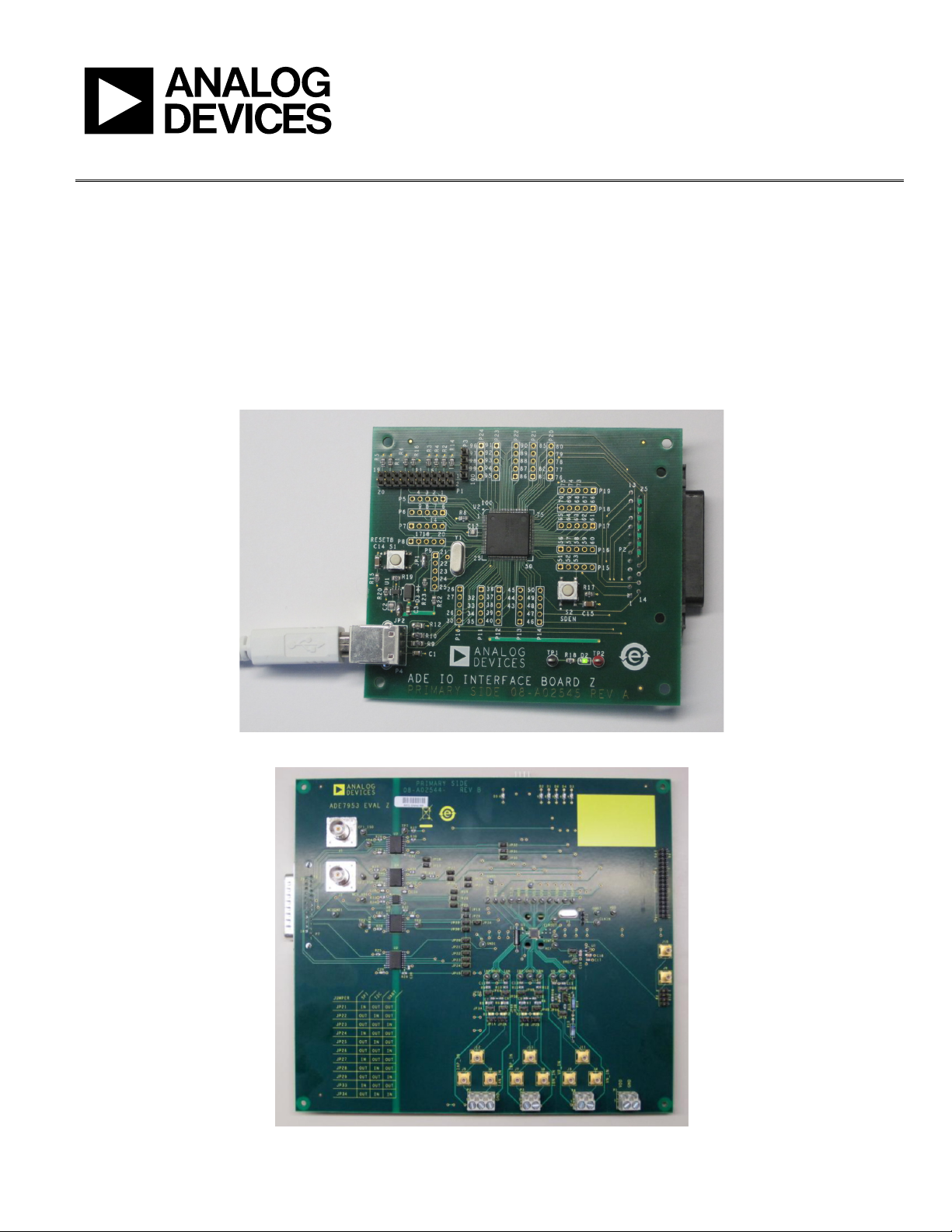
Figure 1. ADE7953 Interface Board
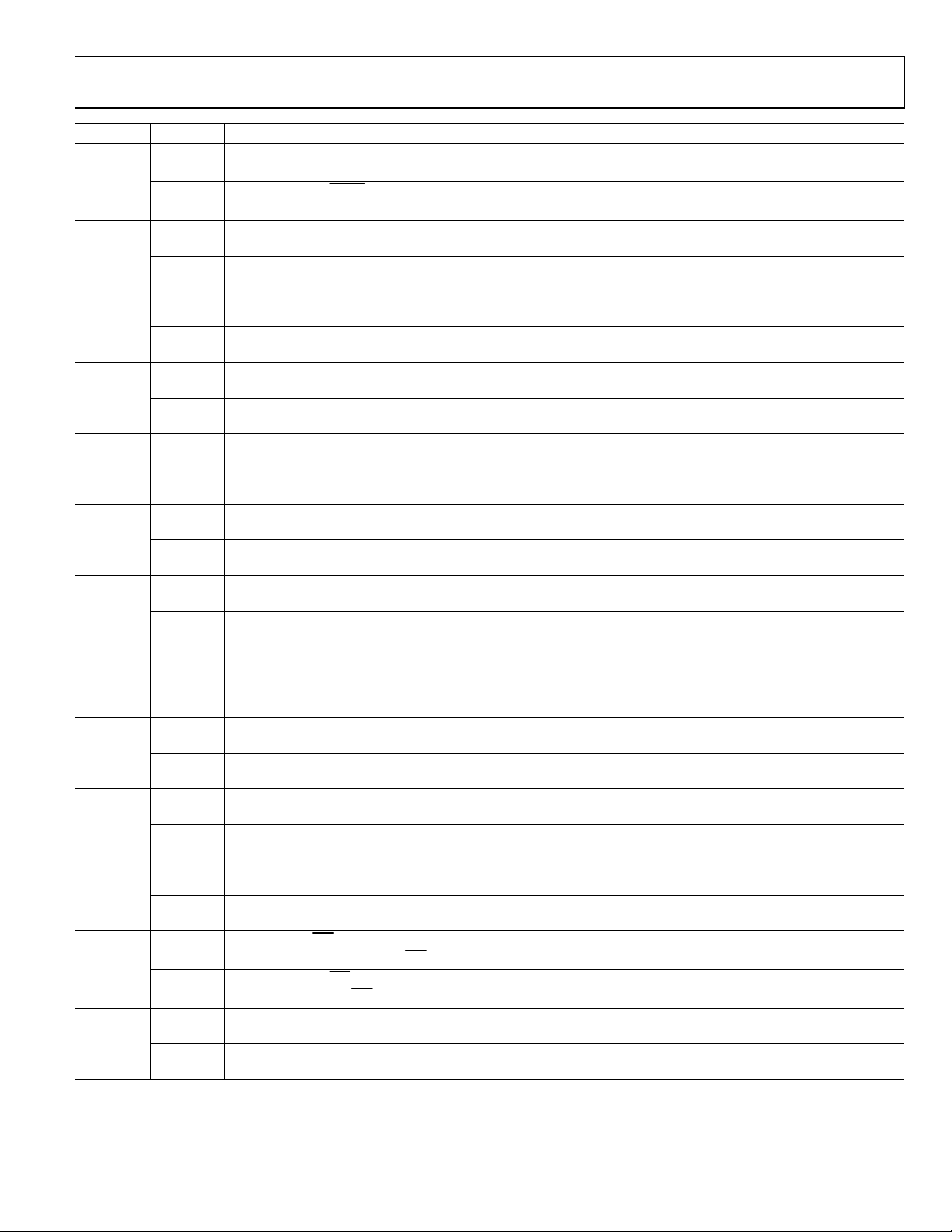
Figure 2. ADE7953 Evaluation Board
09384-001
09384-002

UG-194 Evaluation Board User Guide
TABLE OF CONTENTS
General Description ......................................................................... 1
ADE7953 Interface and Evaluation Boards .................................. 1
Revision History ............................................................................... 2
Evaluation Board Hardware ............................................................ 3
Overview ........................................................................................ 3
Powering Up the Evaluation Board ............................................ 3
Jumper Configuration .................................................................. 3
Installing the Evaluation Board Software ...................................... 7
Installing the Drivers ................................................................... 7
Installing the Evaluation Software ............................................. 8
Running the Evaluation Software ............................................... 8
Troubleshooting the Launch ....................................................... 8
REVISION HISTORY
3/11—Revision 0: Initial Version
Evaluation Software Functions ........................................................9
Active Energy .................................................................................9
Reactive Energy .......................................................................... 10
Apparent Energy ......................................................................... 10
Waveform Sampling ................................................................... 11
ADE7953 Interrupts ................................................................... 11
Power Quality ............................................................................. 11
Read and Write Registers .......................................................... 12
Access All Registers .................................................................... 12
Reset ............................................................................................. 13
Troubleshooting .......................................................................... 13
Evaluation Board Schematics ........................................................ 14
Interface Board Schematics ........................................................... 16
Rev. 0 | Page 2 of 20
Evaluation Board User Guide UG-194
EVALUATION BOARD HARDWARE
OVERVIEW
The ADE7953 evaluation kit includes two boards that should be
used together to evaluate the silicon. The smaller board, named
ADE IO INTERFACE BOARD Z (the interface board), consists
of an NXP LPC2368FBD100 microcontroller that handles all
communications from the PC to the ADE7953 (see Figure 1).
The larger board, named EVAL-ADE7953EBZ (the evaluation
board), includes the ADE7953 energy metering IC, associated
filtering, and isolation to allow high voltage inputs to be used
(see Figure 2). The two boards should be connected together
using the 25-pin connector included in the evaluation kit. The
connector is labeled P2 on the interface board and P7 on the
evaluation board.
Full schematics of the ADE7953 evaluation board and interface
board are provided in the Evaluation Board Schematics section
and the Interface Board Schematics section.
Table 1. Jumper Configuration
Jumper Option Description
JP1A Closed
Open
(default)
JP1B Closed
Open
(default)
JP2A Closed
Open
(default)
JP2B Closed
Open
(default)
JP3A Closed Disables the antialiasing filter (composed of R5 and C7) in the IAP signal path.
Open
(default)
JP3B Closed Disables the antialiasing filter (composed of R7 and C9) in the IBP signal path.
Open
(default)
JP4A Closed Disables the antialiasing filter (composed of R6 and C8) in the IAN signal path.
Open
(default)
JP4B Closed Disables the antialiasing filter (composed of R8 and C10) in the IBN signal path.
Open
(default)
JP5A
Closed
(default)
Open Enables the antialiasing filter (composed of R9 and C11) in the IAP signal path.
Connects Pin 1 of the Channel IA pin connector (P2) to AGND. Use this configuration in conjunction with JP3A and
JP5A closed to short the IAP pin of the ADE7953 to AGND.
Pin 1 of the Channel IA pin connector (P2) is left floating. Use this configuration in normal operation to drive IAP
with analog signal.
Connects Pin 1 of the Channel IB pin connector (P3) to AGND. Use this configuration in conjunction with JP3B and
JP5B closed to short the IBP pin of the ADE7953 to AGND.
Pin 1 of the Channel IB pin connector (P3) is left floating. Use this configuration in normal operation to drive IBP
with analog signal.
Connects Pin 2 of the Channel IA pin connector (P2) to AGND. Use this configuration in conjunction with JP4A and
JP6A closed to short the IAN pin of the ADE7953 to AGND, which should be done when using a shunt current
sensor.
Pin 2 of the Channel IA pin connector (P2) is left floating. Use this configuration when driving a differential input
to IAN, which should be done when using a current transformer or Rogowski coil sensor.
Connects Pin 2 of the Channel IB pin connector (P3) to AGND. Use this configuration in conjunction with JP4B and
JP6B closed to short the IBN pin of the ADE7953 to AGND, which should be done when using a shunt current
sensor.
Pin 2 of the Channel IB pin connector (P3) is left floating. Use this configuration when driving a differential input to
IBN, which should be done when using a current transformer or Rogowski coil sensor.
Enables the antialiasing filter (composed of R5 and C7) in the IAP signal path.
Enables the antialiasing filter (composed of R7 and C9) in the IBP signal path.
Enables the antialiasing filter (composed of R6 and C8) in the IAN signal path.
Enables the antialiasing filter (composed of R8 and C10) in the IBN signal path.
Disables the antialiasing filter (composed of R9 and C11) in the IAP signal path.
POWERING UP THE EVALUATION BOARD
The ADE7953 interface board receives power via the USB
cable that is connected to the PC. No additional power source
is required for the interface board.
The ADE7953 evaluation board requires a 3.3 V power supply.
This power source supplies the nonisolated side of the circuit,
including the ADE7953 energy metering IC and associated
circuitry. The 3.3 V supply should be provided on P1. The
isolated portion of the evaluation board is powered by the
interface board connection.
JUMPER CONFIGURATION
Tabl e 1 describes the jumpers included on the ADE7953 evaluation board and the required settings for different configurations.
Before connecting any high voltage signals, users should review
the jumper configuration and verify that it is correct for their
specific setup.
Rev. 0 | Page 3 of 20

UG-194 Evaluation Board User Guide
Jumper Option Description
JP5B
Closed
(default)
Open Enables the antialiasing filter (composed of R11 and C13) in the IBP signal path.
JP6A
Closed
(default)
Open Enables the antialiasing filter (composed of R10 and C12) in the IAN signal path.
JP6B
Closed
(default)
Open Enables the antialiasing filter (composed of R12 and C14) in the IBN signal path.
JP7A Closed
Open
(default)
JP8A Closed
Open
(default)
JP8B
Closed
(default)
Open
JP9A
Closed
(default)
Open Pin 2 of the Channel V pin connector (P4) is left floating. Use this configuration to drive VN with a differential signal.
JP11 Closed
Open
(default)
JP13
1, 2
(default)
2, 3
JP15
Closed
(default)
Open
JP16
Closed
(default)
Open
JP17
Closed
(default)
Open
JP18
Closed
(default)
Open
JP19
Closed
(default)
Open
Disables the antialiasing filter (composed of R11 and C13) in the IBP signal path.
Disables the antialiasing filter (composed of R10 and C12) in the IAN signal path.
Disables the antialiasing filter (composed of R12 and C14) in the IBN signal path.
Connects Pin 1 of the Channel V pin connector (P4) to AGND. Use this configuration in conjunction with JP8A
closed to connect the VP pin of the ADE7953 to AGND via 1 kΩ Resistor R15.
Pin 1 of the Channel V pin connector (P4) is left floating. Use this configuration in normal operation to drive VP
with analog signal.
Disables the 1000:1 attenuator network (composed of R13, R14, R15, and R17) when JP8B is open. Use this
configuration when using a low voltage signal source on the voltage channel.
Enables the 1000:1 attenuator network (composed of R13, R14, R15, and R17) when JP8B is closed. Use this
configuration when using a high voltage signal source on the voltage channel.
Enables the 1000:1 attenuator network (composed of R13, R14, R15, and R17) when JP8A is open. Use this
configuration when using a high voltage signal source on the voltage channel.
Disables the 1000:1 attenuator network (composed of R13, R14, R15, and R17) when JP8A is closed. Use this
configuration when using a low voltage signal source on the voltage channel.
Connects Pin 2 of the Channel V pin connector (P4) to AGND. Use this configuration to connect the VN pin of the
ADE7953 to AGND via 1 kΩ Resistor R16, which should be done when normal single-ended signals are connected
to the ADE7953 voltage channel.
Connects the ADR280 voltage reference to the REF pin of the ADE7953. Use this configuration when the ADE7953
is configured to use an external reference.
Disconnects the ADR280 voltage reference from the REF pin of the ADE7953. Use this configuration in normal
operation when the ADE7953 is configured to use the internal reference.
Connects Pin 1 of the on-board 3.579545 MHz Crystal Y1 to the CLKIN pin of the ADE7953. Use this configuration
when External Crystal Y1 is used as the clock source for the ADE7953.
Disconnects Pin 1 of the on-board 3.579545 MHz Crystal Y1 from the CLKIN pin of the ADE7953. Use this configuration when an external clock is used. This clock can be connected to Pin 6 of 16×1 Header P5.
Connects the externally applied 3.3 V power to ADuM1401 Isolator U2. Use this configuration in normal operation
when communicating with the ADE7953 via the interface board.
Disconnects the externally applied 3.3 V power to ADuM1401 Isolator U2. Use this configuration when isolation
and/or communication is not required with the ADE7953.
Connects the externally applied 3.3 V power to ADuM1401 Isolator U3. Use this configuration in normal operation
when communicating with the ADE7953 via the interface board.
Disconnects the externally applied 3.3 V power to ADuM1401 Isolator U3. Use this configuration when isolation
and/or communication is not required with the ADE7953.
Connects the externally applied 3.3 V power to ADuM1401 Isolator U4. Use this configuration in normal operation
when communicating with the ADE7953 via the interface board.
Disconnects the externally applied 3.3 V power to ADuM1401 Isolator U4. Use this configuration when isolation
and/or communication is not required with the ADE7953.
Connects the externally applied 3.3 V power to ADuM1401 Isolator U5. Use this configuration in normal operation
when communicating with the ADE7953 via the interface board.
Disconnects the externally applied 3.3 V power to ADuM1401 Isolator U5. Use this configuration when isolation
and/or communication is not required with the ADE7953.
Connects the externally applied 3.3 V power to the ADuM1250 bidirectional isolator, U6. Use this configuration
when communicating with the ADE7953 via the interface board using I
Disconnects the externally applied 3.3 V power to the ADuM1250 bidirectional isolator, U6. Use this configuration
when isolation and/or I
2
C communication is not required with the ADE7953.
2
C.
Rev. 0 | Page 4 of 20
Evaluation Board User Guide UG-194
Jumper Option Description
JP20
Closed
(default)
Open
JP21
Closed
(default)
Open
JP22 Closed
Open
(default)
JP23 Closed
Open
(default)
JP24
Closed
(default)
Open
JP25 Closed
Open
(default)
JP26 Closed
Open
(default)
JP27
Closed
(default)
Open
JP28 Closed
Open
(default)
JP29 Closed
Open
(default)
JP30
Closed
(default)
Open
JP31
Closed
(default)
Open
JP32
Closed
(default)
Open
Connects the RESET
software management of the
Disconnects the RESET
management of the
Connects the SCLK pin of the ADE7953 to ADuM1401 Isolator U3. Use this configuration when communicating
with the ADE7953 via the interface board using SPI.
Disconnects the SCLK pin of the ADE7953 from ADuM1401 Isolator U3. Use this configuration when SPI communication is not required with the ADE7953.
Connects the SCLK pin of the ADE7953 to the externally applied 3.3 V power. Use this configuration when setting
up the ADE7953 to use I2C communication.
Disconnects the SCLK pin of the ADE7953 from the externally applied 3.3 V power. Use this configuration when I2C
communication is not required.
Connects the SCLK pin of the ADE7953 to AGND. Use this configuration when setting up the ADE7953 to use UART
communication.
Disconnects the SCLK pin of the ADE7953 from AGND. Use this configuration when UART communication is not
required.
Connects the MOSI/SCL/Rx pin of the ADE7953 to the MOSI pin on the interface board via ADuM1401 Isolator U4.
Use this configuration when the ADE7953 is set up for SPI communication.
Disconnects the MOSI/SCL/Rx pin of the ADE7953 from the MOSI pin on the interface board via ADuM1401
Isolator U4. Use this configuration when the ADE7953 is not set up for SPI communication.
Connects the MOSI/SCL/Rx pin of the ADE7953 to the SCL pin on the interface board via the ADuM1250 bidirectional
isolator, U6. Use this configuration when the ADE7953 is set up for I
Disconnects the MOSI/SCL/Rx pin of the ADE7953 from the SCL pin on the interface board via the ADuM1250
bidirectional isolator, U6. Use this configuration when the ADE7953 is not set up for I
Connects the MOSI/SCL/Rx pin of the ADE7953 to the TX pin on the interface board via ADuM1401 Isolator U5.
Use this configuration when the ADE7953 is set up for UART communication.
Disconnects the MOSI/SCL/Rx pin of the ADE7953 from the TX pin on the interface board via ADuM1401 Isolator U5.
Use this configuration when the ADE7953 is not set up for UART communication.
Connects the MISO/SDA/Tx pin of the ADE7953 to the MISO pin on the interface board via ADuM1401 Isolator U2.
Use this configuration when the ADE7953 is set up for SPI communication.
Disconnects the MISO/SDA/Tx pin of the ADE7953 from the MISO pin on the interface board via ADuM1401
Isolator U2. Use this configuration when the ADE7953 is not set up for SPI communication.
Connects the MISO/SDA/Tx pin of the ADE7953 to the SDA pin on the interface board via the ADuM1250
bidirectional isolator, U6. Use this configuration when the ADE7953 is set up for I
Disconnects the MISO/SDA/Tx pin of the ADE7953 from the SDA pin on the interface board via the ADuM1250
bidirectional isolator, U6. Use this configuration when the ADE7953 is not set up for I
Connects the MISO/SDA/Tx pin of the ADE7953 to the RX pin on the interface board via ADuM1401 Isolator U2.
Use this configuration when the ADE7953 is set up for UART communication.
Disconnects the MISO/SDA/Tx pin of the ADE7953 from the RX pin on the interface board via ADuM1401 Isolator U2.
Use this configuration when the ADE7953 is not set up for UART communication.
Connects the ZX pin of the ADE7953 to ADuM1401 Isolator U2. Use this configuration in normal operation when
software management of the ZX pin is done via the interface board and the ADE7953 evaluation software.
Disconnects the ZX pin of the ADE7953 from ADuM1401 Isolator U2. Use this configuration when software
management of the ZX pin is not desired.
Connects the IRQ
software management of the
Disconnects the IRQ
management of the
Connects the ZX_I pin of the ADE7953 to ADuM1401 Isolator U3. Use this configuration in normal operation when
software management of the ZX_I pin is done via the interface board and the ADE7953 evaluation software.
Disconnects the ZX_I pin of the ADE7953 from ADuM1401 Isolator U3. Use this configuration when software
management of the ZX_I pin is not desired.
pin of the ADE7953 to Isolator U2. Use this configuration in normal operation when
RESET
pin of the ADE7953 from Isolator U2. Use this configuration when software
ADuM1401
pin is done via the interface board and the ADE7953 evaluation software.
ADuM1401
RESET pin is not desired.
2
C communication.
2
C communication.
2
C communication.
2
C communication.
pin of the ADE7953 to Isolator U3. Use this configuration in normal operation when
IRQ
pin of the ADE7953 from Isolator U3. Use this configuration when software
ADuM1401
pin is done via the interface board and the ADE7953 evaluation software.
ADuM1401
IRQ pin is not desired.
Rev. 0 | Page 5 of 20
UG-194 Evaluation Board User Guide
Jumper Option Description
JP33
JP34 Closed
JP36
JP37
JP38
Closed
(default)
Open
Open
(default)
Closed
(default)
Open
Closed
(default)
Open
Closed
(default)
Open
Connects the CS pin of the ADE7953 to ADuM1401 Isolator U5. Use this configuration when communicating with
the ADE7953 via the interface board using SPI.
Disconnects the CS pin of the ADE7953 from ADuM1401 Isolator U5. Use this configuration when isolation and/or
SPI communication is not required with the ADE7953.
Connects the CS pin of the ADE7953 to the externally applied 3.3 V power. Use this configuration when using
2
C or UART communication.
either I
Disconnects the CS pin of the ADE7953 from the externally applied 3.3 V power. Use this configuration when the
ADE7953 is configured for SPI communication.
Connects the REVP
software management of the
Disconnects the REVP
management of the
Connects the CF1 pin of the ADE7953 to CF1_ISO BNC Connector J1 via ADuM1401 Isolator U4. Use this configuration
when the isolated interface to CF1 is required.
Disconnects the CF1 pin of the ADE7953 from CF1_ISO BNC Connector J1 via ADuM1401 Isolator U4. Use this
configuration when the isolated interface to CF1 is not required.
Connects the CF2 pin of the ADE7953 to CF2_ISO BNC Connector J2 via ADuM1401 Isolator U5. Use this configuration
when the isolated interface to CF2 is required.
Disconnects the CF2 pin of the ADE7953 from CF2_ISO BNC Connector J2 via ADuM1401 Isolator U5. Use this
configuration when the isolated interface to CF2 is not required.
pin of the ADE7953 to Isolator U4. Use this configuration in normal operation when
REVP pin is done via the interface board and the ADE7953 evaluation software.
pin of the ADE7953 from Isolator U4. Use this configuration when software
REVP
pin is not desired.
ADuM1401
ADuM1401
Rev. 0 | Page 6 of 20

Evaluation Board User Guide UG-194
INSTALLING THE EVALUATION BOARD SOFTWARE
INSTALLING THE DRIVERS
When using the ADE7953 evaluation tools for the first time,
a driver must be installed to allow successful communication.
The driver can be found on the accompanying CD in the folder
VirCOM_Driver_XP.
There are two folders within the VirCOM_Driver_XP folder.
• The Windows XP and VISTA folder contains the driver
suitable for 32-bit operating systems, such as Windows XP
and the 32-bit version of Windows Vista®.
• The Windows 7 (64 bit) folder contains the driver suitable
for 64-bit operating systems, such as Windows 7.
Select the appropriate driver based on the operating system
used on the PC. To install the driver, follow this procedure.
1. Connect the USB cable from the PC to the interface board.
The Found New Hardware Wizard window appears,
indicating that the PC has detected the new hardware.
3. In the Found New Hardware Wizard window (see Figure 3),
select the Install from a list or specific location (Advanced)
option and click Next.
The following window opens (see Figure 4).
Figure 4. Search for Driver Window
4. Select Search removable media (floppy, CD-ROM) and
Include this location in the search (see Figure 4). Use
the Browse button to locate the Windows XP and VISTA
or Windows 7 (64 bit) folder in the VirCOM_Driver_XP
folder on the evaluation kit CD.
5. Click Next.
The Hardware Installation window appears, stating that
the hardware did not pass the Windows Logo test.
09384-004
Figure 3. Found New Hardware Wizard Window
2. If you are installing the driver on a system running
Windows 7, the Found New Hardware Wizard may not
appear. To manually select the driver, follow these steps.
a. Choose Control Panel > Hardware and Sound >
Device Manager; locate the new hardware under the
Ports heading.
b. Right-click the port and select Update Driver
Software.
c. Select Browse my Computer for Driver Software.
The window shown in Figure 4 appears.
d. Go to Step 4.
09384-003
6. Click Continue Anyway.
Rev. 0 | Page 7 of 20
Figure 5. Hardware Installation Window
When the installation is complete, the window shown in
Figure 6 appears.
09384-005

UG-194 Evaluation Board User Guide
When the evaluation software is running, it should automatically detect the COM port that the ADE7953 interface board is
connected to. If the port detection is successful, the COM port
number appears in the Port Control field, as shown in Figure 7
(COM3 in this example).
09384-006
Figure 6. Installation Complete Window
7. Click Finish to close the window.
INSTALLING THE EVALUATION SOFTWARE
The evaluation software is available on the accompanying CD in
the Evaluation Software folder. An executable version of the software is available in the EXE folder. The executable can be run
even if a licensed copy of LabVIEW is not available.
If LabVIEW 2010 will be used on the PC for the first time, an
installer must be run before opening any of the LabVIEW files.
This installer is available in the ADE7953_RevG_Installer
folder. If a copy of LabVIEW 2010 is available on the PC, a full
version of the evaluation code is also provided in the Labview
Source Code – 2010 folder.
To run the LabVIEW 2010 installer, follow these steps:
1. Locate the ADE7953_RevG_Installer folder and
double-click the setup.exe file.
2. Follow the prompts to install the LabVIEW 2010
run-time engine.
Figure 7. Main Window
Note that supply power to the evaluation board is not required
for COM port detection. The interface board is powered from
the USB connection from the PC.
TROUBLESHOOTING THE LAUNCH
If the software does not detect the communications port, the
message shown in Figure 8 is displayed.
09384-007
When the installation is complete, the ADE7953 evaluation
software opens automatically and a shortcut is added to the
Start menu. This shortcut can be found by selecting
Programs > ADE7953_Eval_RevG.
RUNNING THE EVALUATION SOFTWARE
If you do not have a licensed copy of LabVIEW 2010 on the PC,
run the installer, as described in the Installing the Evaluation
Software section.
To run the evaluation software, do one of the following:
• Open the ADE7953_Eval_RevG program from the Start
menu, or open this program from the evaluation software
CD by double-clicking the ADE7953_Eval_RevG.exe file
located in the EXE folder.
• If a licensed copy of LabVIEW 2010 is available on the PC
and you wish to view and edit the code, open the Labview
Source Code – 2010 folder and double-click the
ADE7953_Eval.vi file.
Rev. 0 | Page 8 of 20
09384-008
Figure 8. Comm Port Not Found Message
If this message appears, the following steps should be taken:
1. Click Ye s to return to the main window (see Figure 7).
2. Verify that the interface board is connected to the PC using
the USB cable.
3. Ensure that the required drivers are installed as described
in the Installing the Drivers section.
4. Using the Device Manager tool, ensure that the port is
operating correctly.
5. Manually select the correct COM port by clicking the Port
Control tab in the main window.

Evaluation Board User Guide UG-194
EVALUATION SOFTWARE FUNCTIONS
The ADE7953 evaluation software allows access to all registers
and features of the ADE7953 using SPI, I
2
C, or UART communication. The communication mode and speed should be set in the
main window (see Figure 7). The menu options available are
• Active Energy
• Reactive Energy
• Apparent Energy
• Wave for m S amp ling
• Interrupts
• Power Quality Information
• Read and Write Registers
• Access All Registers
• Reset ADE7953
• EXIT (stops LabVIEW)
These options provide access to all internal registers and allow
the evaluation of ADE7953 performance. To access these functions, click the desired option in the MENU box (see Figure 7).
Clicking an option in the MENU box displays a window where
the specific function can be accessed. Each window includes an
EXIT button that should be used to return to the main window.
Note that only one option from the MENU box can be open at a
time; click EXIT to return to the main window before choosing
another option from the MENU box.
The tabs at the top of the window allow registers associated
with Current Channel A or Current Channel B to be accessed.
A register can be read by clicking READ All Registers. Register
modifications can be made directly on the signal path diagram;
these modifications are written to the part by clicking WRITE
All Registers.
From the Active Energy window, the CF Outputs window can
be accessed by clicking CF Output. Clicking CF Output opens
the window shown in Figure 9.
ACTIVE ENERGY
The Active Energy window is shown in Figure 10. This window
allows access to all registers associated with the active energy
measurement.
Figure 10. Active Energy Window
Figure 9. CF Outputs Window
From this window, the functionality of the CF1 and CF2 output
pins can be selected.
09384-009
09384-010
Rev. 0 | Page 9 of 20

UG-194 Evaluation Board User Guide
The Line Cycle Accumulation window is also accessible from
the Active Energy window (see Figure 11).
Figure 11. Line Cycle Accumulation Window
The line cycle mode allows energy to be accumulated over an
integral number of half line cycles. To activate line cycle accumulation, an ac signal must be present on the voltage channel.
Click EXIT in the CF Outputs or Line Cycle Accumulation
window to return to the Active Energy window.
09384-011
APPARENT ENERGY
The Apparent Energy window is available from the MENU
box. The Apparent Energy window allows access to the registers associated with the apparent energy measurement (see
Figure 13). Tabs are available to select Current Channel A or
Current Channel B registers.
The CF Outputs and Line Cycle Accumulation windows
shown in Figure 9 and Figure 11 are also accessible from
the Apparent Energy window.
Apparent energy measurement is derived from the product
of the current rms and voltage rms measurements. The RMS
window can be accessed from the Apparent Energy window
by clicking Vo lt age R MS or Current RMS (see Figure 12).
REACTIVE ENERGY
The Reactive Energy window is available from the MENU box.
This window is similar to the Active Energy window shown in
Figure 10, but it allows access to registers that are associated
with the reactive energy measurements. Tabs are available to
select Current Channel A or Current Channel B registers. The
CF Outputs and Line Cycle Accumulation windows are also
accessible from the Reactive Energy window (see Figure 9 and
Figure 11, respectively).
Figure 12. RMS Window
From the RMS window, the calibration and configuration registers associated with the VRMS and IRMS measurements can be
accessed. In addition, the rms readings can be obtained. Click
EXIT in this window to return to the Apparent Energy window.
09384-013
09384-012
Figure 13. Apparent Energy Window
Rev. 0 | Page 10 of 20

Evaluation Board User Guide UG-194
WAVEFORM SAMPLING
The Wave for m Sam pli ng window is available from the MENU
box. The Wav efo rm Sa mpl in g window is shown in Figure 14.
To use th e Wave for m S amp lin g window, SPI must be selected
as the communication interface (see Figure 7).
The switch buttons in the ADE7953 Interrupts window allow
the individual interrupt enable bits to be selected. After the
appropriate interrupt enable bits are selected, they can be
written to the part by clicking Writ e IR Q Ena ble Re gis ter.
The lights represent the corresponding interrupt status registers.
These registers can be read and reset by clicking Read IRQ Status
or Read IRQ Status with Reset.
POWER QUALITY
The Power Quality window is available from the MENU box.
The Power Quality window is shown in Figure 16.
Figure 14. Waveform Sampling Window
This window allows raw waveform data to be captured and
displayed on a graph. To save the data to a file, click the Store
data to file? toggle switch and enter a destination file name in
the adjacent box.
ADE7953 INTERRUPTS
The ADE7953 Interrupts window is available from the MENU
box. The ADE7953 Interrupts window is shown in Figure 15.
Figure 15. ADE7953 Interrupts Window
This window allows access to the status and enable registers
associated with the Current Channel A, Current Channel B,
and voltage channel interrupts.
Rev. 0 | Page 11 of 20
09384-016
Figure 16. Power Quality Window
09384-014
The following features can be configured using the Power
Quality window:
• Peak detection
• Sag detection
• No-load detection
• Zero-crossing detection
• Power factor measurement
• Angle measurement
• Reverse power
The tabs in the Power Quality window are used to select
the appropriate feature. Each feature can be configured and
then written to the part by clicking WRITE. The ADE7953
Interrupts window shown in Figure 15 can be accessed from
the Power Quality window by clicking IRQ’s.
09384-015

UG-194 Evaluation Board User Guide
READ AND WRITE REGISTERS
The Read and Write Registers window is available from the
MENU box. The Read and Write Registers window is shown
in Figure 17.
Figure 17. Read and Write Registers Window
An individual register can be accessed from this window by
selecting the register name from the pull-down menu. Alternatively, registers can be accessed by address by clicking the
Register Name toggle switch and then typing the address and
size of a register into the register address and register size boxes.
09384-017
ACCESS ALL REGISTERS
The Access All Registers window is available from the MENU
box. The Access All Registers window allows all the registers in
the ADE7953 to be accessed at once (see Figure 18).
Figure 18. Access All Registers Window
The entire ADE7953 register bank can be read or modified
by clicking READ All Registers or WRITE All Registers. The
current configuration can be saved to a comma-separated
variable (.csv) file by specifying a destination file at the top
of the window and then clicking Save Current Register
Settings to File.
To load a configuration from a file, specify a configuration file
at the top of the window and then click Load Register Settings
from File. The contents of the specified .csv file are written to
the ADE7953.
09384-018
Rev. 0 | Page 12 of 20

Evaluation Board User Guide UG-194
RESET
The Reset window is available from the MENU box. The Reset
window is shown in Figure 19.
Figure 21. Clear Port Window
When the Clear Port window appears, press the S1 push-button
located above the PC connection on the ADE7953 interface port
to reset the PC COM port (see Figure 1). After completing this
action, click DONE in the Clear Port window.
09384-019
Figure 19. Reset Window
When the RESET ADE7953 button is clicked, a hardware reset
is performed on the ADE7953. All register data is lost and the
part must be reconfigured.
Before continuing with the evaluation of the ADE7953, the
reason for the communication failure should be investigated.
After the COM port is cleared, the window shown in Figure 22
is displayed to provide some possible reasons for the failed
communication.
09384-021
TROUBLESHOOTING
Communication Failure
If communication to the ADE7953 is not successful, the warning
message shown in Figure 20 is displayed.
09384-020
Figure 20. Communication Unsuccessful Message
This message indicates that the ADE7953 did not respond
and the communication timed out. The communication port
on the PC must be reset to restore communication to the
ADE7953. When the OK button is clicked, the Clear Port
window appears (see Figure 21).
09384-022
Figure 22. Error Debug Window
After clicking OK, click EXIT in the main window (see Figure 7).
To troubleshoot the problem, verify the following items:
• The selected COM port is correct in the main window (see
Figure 7).
• The currently configured communication mode is correct
in the main window (see Figure 7).
• The correct jumpers are installed for the selected commu-
nication interface (see Tabl e 1).
Incorrect Register Readings
If the data read back from the ADE7953 registers is always
FFFF, a possible cause is that the ADE7953 is not correctly
powered. Ensure that a 3.3 V supply has been supplied to the
ADE7953, as described in the Powering Up the Evaluation
Board section.
Rev. 0 | Page 13 of 20

UG-194 Evaluation Board User Guide
EVALUATION BOARD SCHEMATICS
09384-023
Figure 23. Evaluation Board Schematic (Page 1)
Rev. 0 | Page 14 of 20

Evaluation Board User Guide UG-194
0
9384-024
Figure 24. Evaluation Board Schematic (Page 2)
Rev. 0 | Page 15 of 20

UG-194 Evaluation Board User Guide
INTERFACE BOARD SCHEMATICS
09384-025
Figure 25. Interface Board Schematic (Page 1)
Rev. 0 | Page 16 of 20

Evaluation Board User Guide UG-194
09384-026
Figure 26. Interface Board Schematic (Page 2)
Rev. 0 | Page 17 of 20

UG-194 Evaluation Board User Guide
NOTES
Rev. 0 | Page 18 of 20

Evaluation Board User Guide UG-194
NOTES
Rev. 0 | Page 19 of 20

UG-194 Evaluation Board User Guide
NOTES
ESD Caution
ESD (electrostatic discharge) sensitive device. Charged devices and circuit boards can discharge without detection. Although this product features patented or proprietary protection
circuitry, damage may occur on devices subjected to high energy ESD. Therefore, proper ESD precautions should be taken to avoid performance degradation or loss of functionality.
Legal Terms and Conditions
By using the evaluation board discussed herein (together with any tools, components documentation or support materials, the “Evaluation Board”), you are agreeing to be bound by the terms and conditions
set forth below (“Agreement”) unless you have purchased the Evaluation Board, in which case the Analog Devices Standard Terms and Conditions of Sale shall govern. Do not use the Evaluation Board until you
have read and agreed to the Agreement. Your use of the Evaluation Board shall signify your acceptance of the Agreement. This Agreement is made by and between you (“Customer”) and Analog Devices, Inc.
(“ADI”), with its principal place of business at One Technology Way, Norwood, MA 02062, USA. Subject to the terms and conditions of the Agreement, ADI hereby grants to Customer a free, limited, personal,
temporary, non-exclusive, non-sublicensable, non-transferable license to use the Evaluation Board FOR EVALUATION PURPOSES ONLY. Customer understands and agrees that the Evaluation Board is provided
for the sole and exclusive purpose referenced above, and agrees not to use the Evaluation Board for any other purpose. Furthermore, the license granted is expressly made subject to the following additional
limitations: Customer shall not (i) rent, lease, display, sell, transfer, assign, sublicense, or distribute the Evaluation Board; and (ii) permit any Third Party to access the Evaluation Board. As used herein, the term
“Third Party” includes any entity other than ADI, Customer, their employees, affiliates and in-house consultants. The Evaluation Board is NOT sold to Customer; all rights not expressly granted herein, including
ownership of the Evaluation Board, are reserved by ADI. CONFIDENTIALITY. This Agreement and the Evaluation Board shall all be considered the confidential and proprietary information of ADI. Customer may
not disclose or transfer any portion of the Evaluation Board to any other party for any reason. Upon discontinuation of use of the Evaluation Board or termination of this Agreement, Customer agrees to
promptly return the Evaluation Board to ADI. ADDITIONAL RESTRICTIONS. Customer may not disassemble, decompile or reverse engineer chips on the Evaluation Board. Customer shall inform ADI of any
occurred damages or any modifications or alterations it makes to the Evaluation Board, including but not limited to soldering or any other activity that affects the material content of the Evaluation Board.
Modifications to the Evaluation Board must comply with applicable law, including but not limited to the RoHS Directive. TERMINATION. ADI may terminate this Agreement at any time upon giving written notice
to Customer. Customer agrees to return to ADI the Evaluation Board at that time. LIMITATION OF LIABILITY. THE EVALUATION BOARD PROVIDED HEREUNDER IS PROVIDED “AS IS” AND ADI MAKES NO
WARRANTIES OR REPRESENTATIONS OF ANY KIND WITH RESPECT TO IT. ADI SPECIFICALLY DISCLAIMS ANY REPRESENTATIONS, ENDORSEMENTS, GUARANTEES, OR WARRANTIES, EXPRESS OR IMPLIED, RELATED
TO THE EVALUATION BOARD INCLUDING, BUT NOT LIMITED TO, THE IMPLIED WARRANTY OF MERCHANTABILITY, TITLE, FITNESS FOR A PARTICULAR PURPOSE OR NONINFRINGEMENT OF INTELLECTUAL
PROPERTY RIGHTS. IN NO EVENT WILL ADI AND ITS LICENSORS BE LIABLE FOR ANY INCIDENTAL, SPECIAL, INDIRECT, OR CONSEQUENTIAL DAMAGES RESULTING FROM CUSTOMER’S POSSESSION OR USE OF
THE EVALUATION BOARD, INCLUDING BUT NOT LIMITED TO LOST PROFITS, DELAY COSTS, LABOR COSTS OR LOSS OF GOODWILL. ADI’S TOTAL LIABILITY FROM ANY AND ALL CAUSES SHALL BE LIMITED TO THE
AMOUNT OF ONE HUNDRED US DOLLARS ($100.00). EXPORT. Customer agrees that it will not directly or indirectly export the Evaluation Board to another country, and that it will comply with all applicable
United States federal laws and regulations relating to exports. GOVERNING LAW. This Agreement shall be governed by and construed in accordance with the substantive laws of the Commonwealth of
Massachusetts (excluding conflict of law rules). Any legal action regarding this Agreement will be heard in the state or federal courts having jurisdiction in Suffolk County, Massachusetts, and Customer hereby
submits to the pers onal jurisdiction and venu e of such courts. The United Nations Conventi on on Contracts for the Internation al Sale of Goods shall not apply to this Agreement and is expressly disclaimed.
©2011 Analog Devices, Inc. All rights reserved. Trademarks and
registered trademarks are the property of their respective owners.
UG09384-0-3/11(0)
Rev. 0 | Page 20 of 20
 Loading...