

Evaluation Board User Guide
One Technology Way • P. O . Box 9106 • Norwood, MA 02062-9106, U.S.A. • Tel : 781.329.4700 • Fax : 781.461.3113 • www.analog.com
UG-177
Evaluating the ADAU1781 SigmaDSP using the EVAL-ADAU1781Z
EVAL-ADAU1781Z PACKAGE CONTENTS
ADAU1781 evaluation board
EVAL-ADUSB2EBZ (USBi) communications adapter
USB cable with Mini-B plug
Evaluation board/software quick-start guide
DOCUMENTS NEEDED
ADAU1781 data sheet
ADMP401 data sheet
AN-1006 Applications Note, Using the EVAL-ADUSB2EBZ
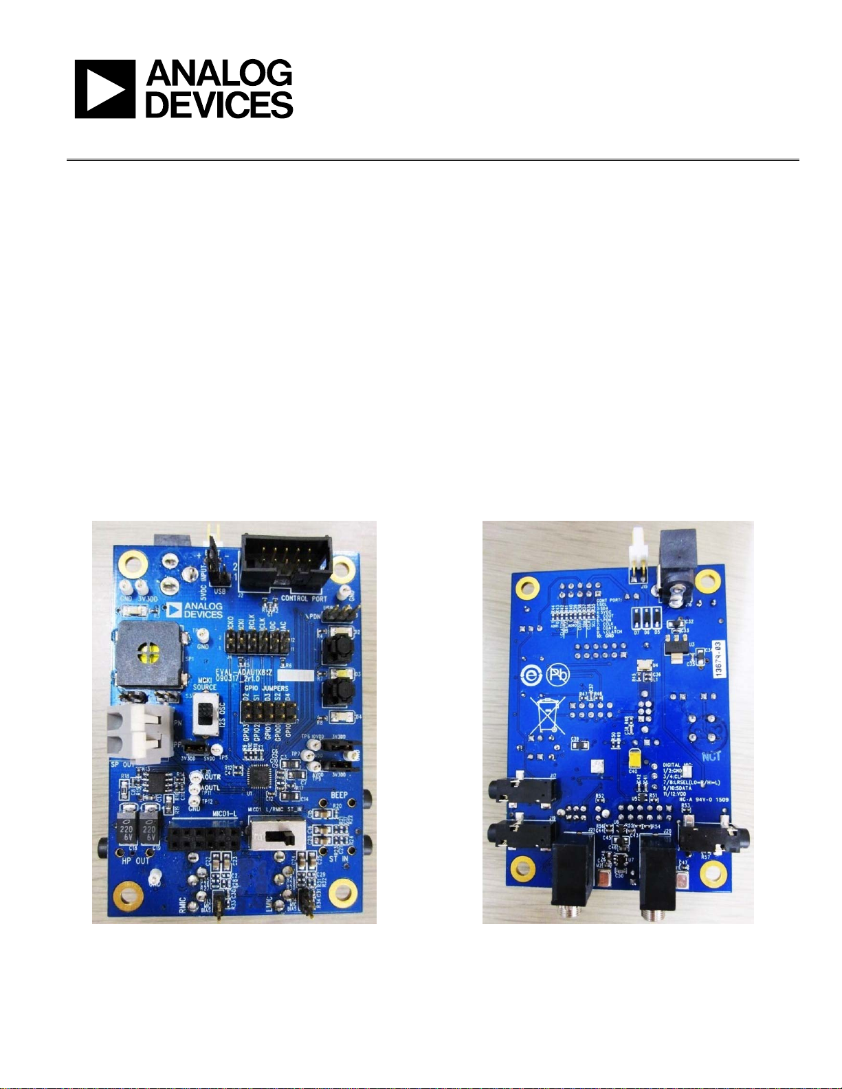
EVALUATION BOARD TOP SIDE AND BOTTOM SIDE
GENERAL DESCRIPTION
This user guide explains the design and setup of the ADAU1781
SigmaDSP® evaluation board.
This evaluation board provides full access to all analog and digital
I/Os on the ADAU1781. The SigmaDSP is controlled by Analog
Devices, Inc., SigmaStudio™ software, which interfaces to the
board via a USB connection. This evaluation board can be
powered either over the USB bus or by a single 3.8 V to 6 V
supply, which is regulated to the voltages required on the board.
The PC board is a 4-layer design, with a single ground plane and a
single power plane on the inner layers. The board contains onboard microphones and speaker, and connectors for external
microphones and speaker. The master clock can be provided
externally or by the on-board 12.288 MHz active oscillator.
Figure 1. Evaluation Board Top Side
PLEASE SEE THE LAST PAGE FOR AN IMPORTANT
WARNING AND LEGAL TERMS AND CONDITIONS.
08314-001
Rev. 0 | Page 1 of 24
08314-002
Figure 2. Evaluation Board Bottom Side

UG-177 Evaluation Board User Guide
TABLE OF CONTENTS
EVAL-ADAU1781Z Package Contents .......................................... 1
Documents Needed .......................................................................... 1
General Description ......................................................................... 1
Evaluation Board Top Side and Bottom Side ................................ 1
Revision History ............................................................................... 2
Evaluation Board Block Diagrams ................................................. 3
Setting Up the Evaluation Board .................................................... 5
Installing the SigmaStudio Software .......................................... 5
Installing the USBi Drivers ......................................................... 5
Default Switch and Jumper Settings .......................................... 5
Powering Up the Board ............................................................... 6
Connecting the Audio Cables ..................................................... 6
Setting Up Communications in SigmaStudio ........................... 6
Configuring the Registers ........................................................... 6
Creating a Basic Signal Flow ........................................................7
Downloading the Program to the DSP.................................... 10
Using the Evaluation Board .......................................................... 11
Power ............................................................................................ 11
Master Clock ............................................................................... 11
Inputs and Outputs .................................................................... 11
GPIO ............................................................................................ 11
Serial Audio Interface ................................................................ 11
Communications Header .......................................................... 11
Power-Down ............................................................................... 11
Evaluation Board Schematics and Artwork ................................ 12
Ordering Information .................................................................... 21
Bill of Materials ........................................................................... 21
REVISION HISTORY
7/10—Revision 0: Initial Version
Rev. 0 | Page 2 of 24
Evaluation Board User Guide UG-177
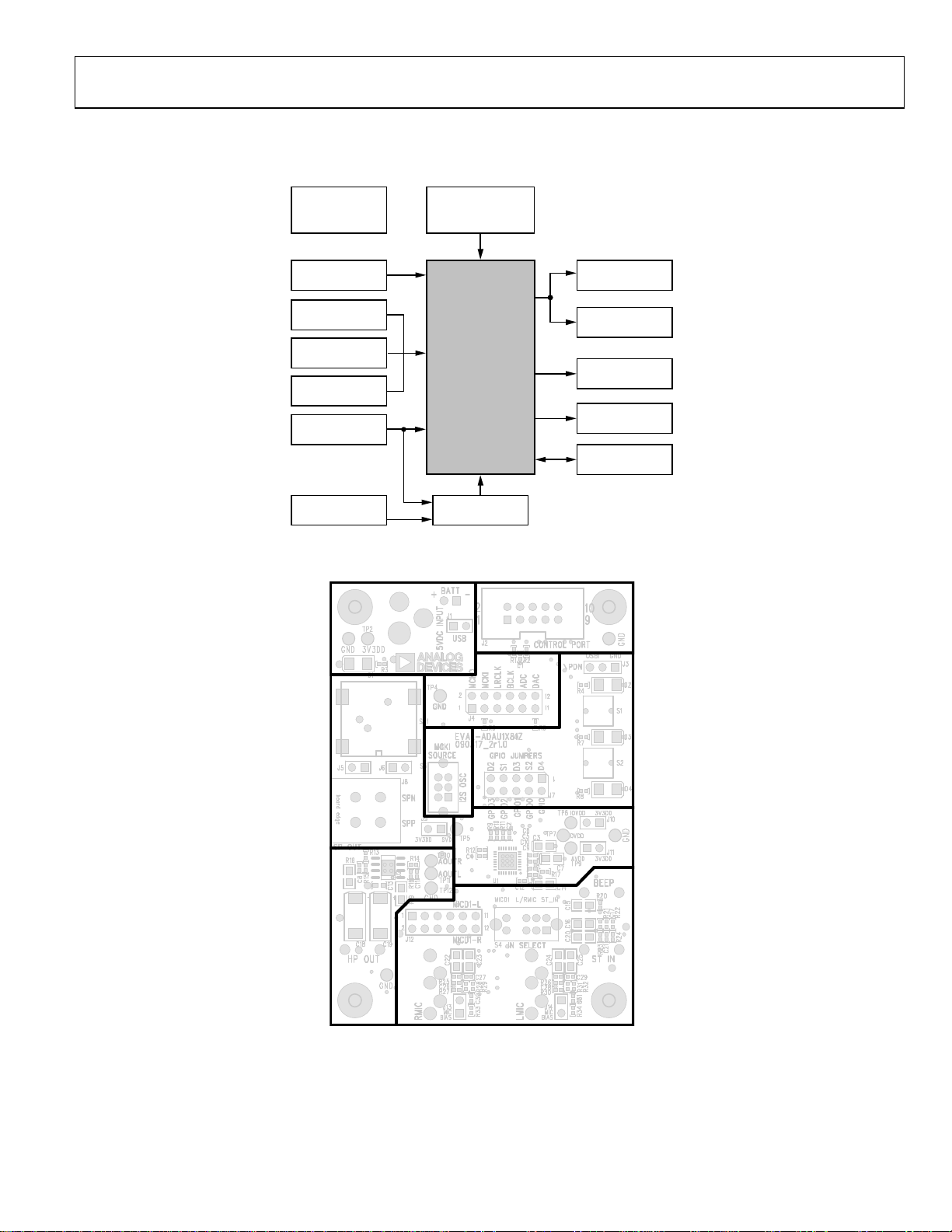
EVALUATION BOARD BLOCK DIAGRAMS
POWER
SUPPLY
REGULATION
BEEP
INPUT
ANALOG MI C
INPUTS
STEREO LINE
INPUT
DIGITAL MIC
INPUTS
SERIAL AUDIO
CONNECTOR
ACTIVE
OSCILLATOR
I2S/SPI
COMMUNICATIONS
HEADER
ADAU1781
SigmaDSP
MASTER CLOCK
SELECTOR
SPEAKER
CONNECTOR
ON-BOARD
SPEAKER
HEADPHONE
OUTPUT
SERIAL AUDIO
CONNECTOR
GPIO
08314-003
Figure 3. Functional Block Diagram
POWER
COMMUNICATIONS
HEADER
SERIAL AUDI O
CONNECTOR
SPEAKER
GPIO
MCLK
SPEAKER
OUTPUTS
HEADPHONE
OUTPUT
SELECT
ADAU1781
SigmaDSP
BEEP/MIC/STEREO LINE
INPUTS
08314-004
Figure 4. Board Layout Block Diagram
Rev. 0 | Page 3 of 24
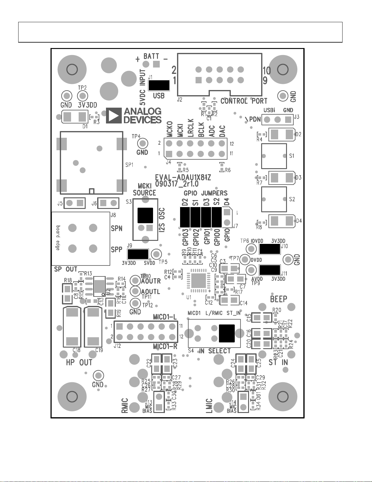
UG-177 Evaluation Board User Guide
OSC
ST
IN
08314-005
Figure 5. Default Jumper and Switch Settings (A Solid Black Rectangle Indicates a Switch or Jumper Position)
Rev. 0 | Page 4 of 24

Evaluation Board User Guide UG-177
SETTING UP THE EVALUATION BOARD
INSTALLING THE SigmaStudio SOFTWARE
Users can download the latest version of SigmaStudio by
completing the following steps:
1. Go to www.analog.com/sigmastudiodownload and fill in
the Email: and Software Key: boxes. You will get a
software key with the evaluation board, or you can contact
Analog Deviecs, Inc., at sigmadsp@analog.com to request a
software key.
2. Chose which version of SigmaStudio you would like and
click Submit.
3. Download the installer file, open the file, and extract the
files to your PC.
4. Install the Microsoft .NET Framework if you do not
already have it installed.
5. Install SigmaStudio by double-clicking setup.exe and
follow the prompts.
Click Search for the best driver in these locations, select
Include this location in the search, and click Browse to find
the SigmaStudio 3.0\USB drivers directory (see Figure 8).
INSTALLING THE USBi DRIVERS
SigmaStudio must be installed to use the USBi. When
SigmaStudio has been properly installed, connect the USBi
to an available USB port with the included USB cable. At this
point, Windows® XP recognizes the device and prompts the
user to install drivers (see Figure 6).
08314-006
Figure 6. Found New Hardware Notification
Select the Install from a list or specific location (Advanced)
option and click Next > (see Figure 7).
Figure 8. Windows Found New Hardware Wizard—Search and
Installation Options
When the warning about Windows Logo testing appears, click
Continue Anyway (see Figure 9).
Figure 9. Windows Logo Testing Warning
The USBi drivers should now be installed successfully. Leave
the USBi connected to the PC.
08314-008
08314-009
Figure 7. Found New Hardware Wizard—Installation
DEFAULT SWITCH AND JUMPER SETTINGS
By default, the evaluation board is configured for single-ended
8314-007
Rev. 0 | Page 5 of 24
stereo analog input and headphone output.
The J1, J10, J11, J13, and J14 jumpers must be connected. The
GPIO jumper (J7) can be connected as desired to use GPIO
circuitry.
Switch S3 (MCKI SOURCE) should be in the up (OSC)
position, and Switch S4 (IN SELECT) should be in the
right (ST_IN) position.
UG-177 Evaluation Board User Guide
POWERING UP THE BOARD
To power up the board, connect the ribbon cable of the USBi
to J2 (CONTROL PORT) of the EVAL-ADAU1781Z.
CONNECTING THE AUDIO CABLES
Connect a stereo audio source to J19 (ST IN). Connect headphones or powered speakers to J18 (HP OUT). The labels for
J18 and J19 are only visible on the bottom of the board.
SETTING UP COMMUNICATIONS IN SIGMASTUDIO
Start SigmaStudio by double-clicking the shortcut on the desktop.
Click File…New Project or press Ctrl+N to create a new project.
The default view of the new project is called the Hardware
Configuration tab.
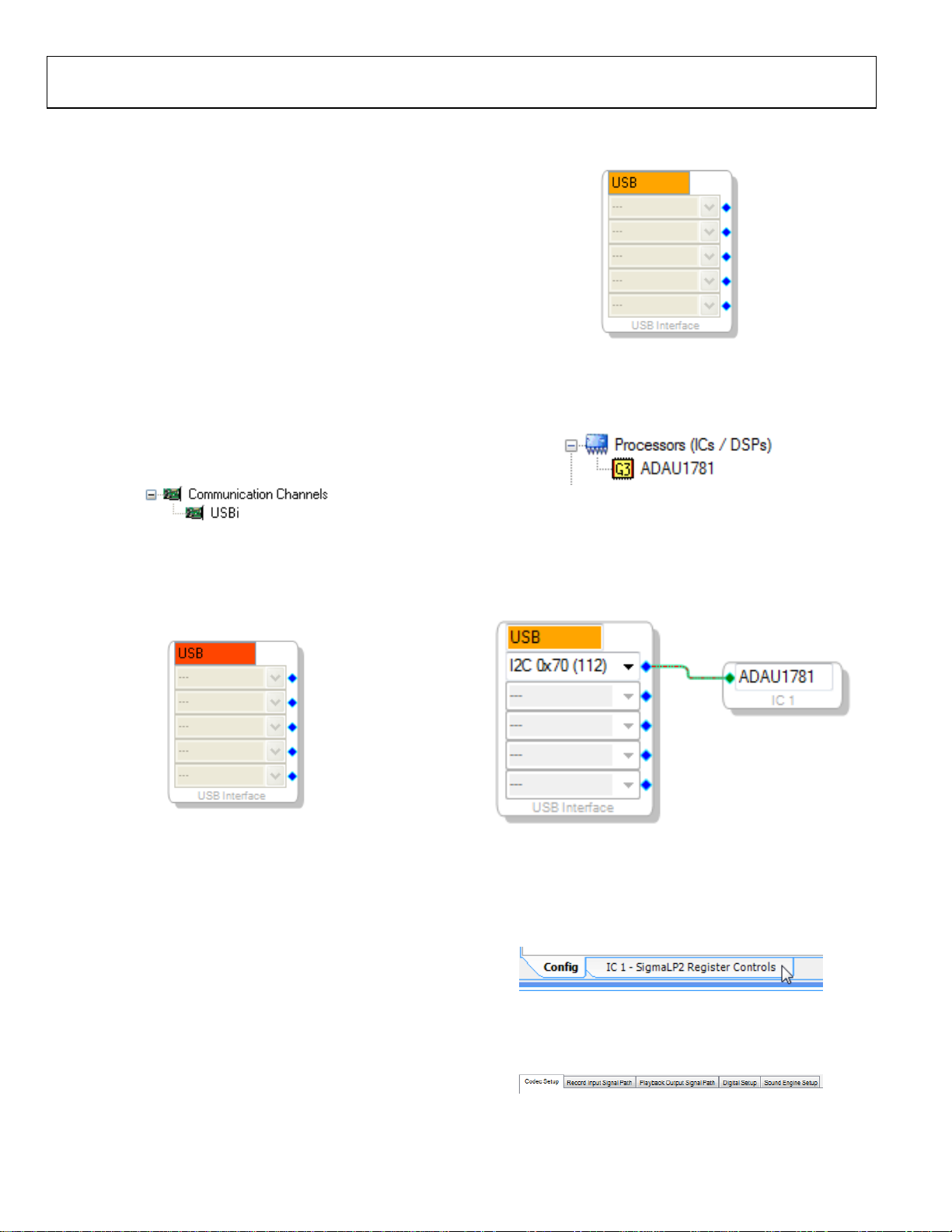
To use the USBi in conjunction with SigmaStudio, first select it
in the Communication Channels subsection of the toolbox on the
left side of the Hardware Configuration tab, and add it to the project
space by clicking and dragging it to the right (see Figure 10).
08314-010
Figure 10. Adding the USBi Communication Channel
If SigmaStudio cannot detect the USBi on the USB port of the
computer, then the background of the USB label will be red
(see Figure 11). This may happen when the USBi is not connected
or when the drivers are incorrectly installed.
If SigmaStudio detects the USBi on the USB port of the computer,
the background of the USB label changes to orange (see Figure 12).
08314-012
Figure 12. USBi Detected by SigmaStudio
To add an ADAU1781 to the project, select it from the
Processors (ICs / DSPs) list and drag it to the project space
(see Figure 13).
08314-013
Figure 13. Adding an ADAU1781
To use the USB interface to communicate with the target IC,
connect it by clicking and dragging a wire between the blue pin
of the USBi and the green pin of the IC (see Figure 14). The
corresponding drop-down box of the USBi automatically fills
with the default mode and channel for that IC.
08314-011
Figure 11. USBi Not Detected by SigmaStudio
CONFIGURING THE REGISTERS
To access the graphical register control window, click the IC 1 –
SigmaLP2 Register Controls tab near the bottom of the
window (see Figure 15).
Within the register control view, there are several tabs at the top
for easy navigation. Start with the Codec Setup tab (see Figure 16).
Rev. 0 | Page 6 of 24
Figure 14. Connecting the USB Interface to an ADAU1781 IC
Figure 15. Register Control Tab
Figure 16. Codec Setup Register Tab
08314-014
08314-015
08314-016
Evaluation Board User Guide UG-177
9
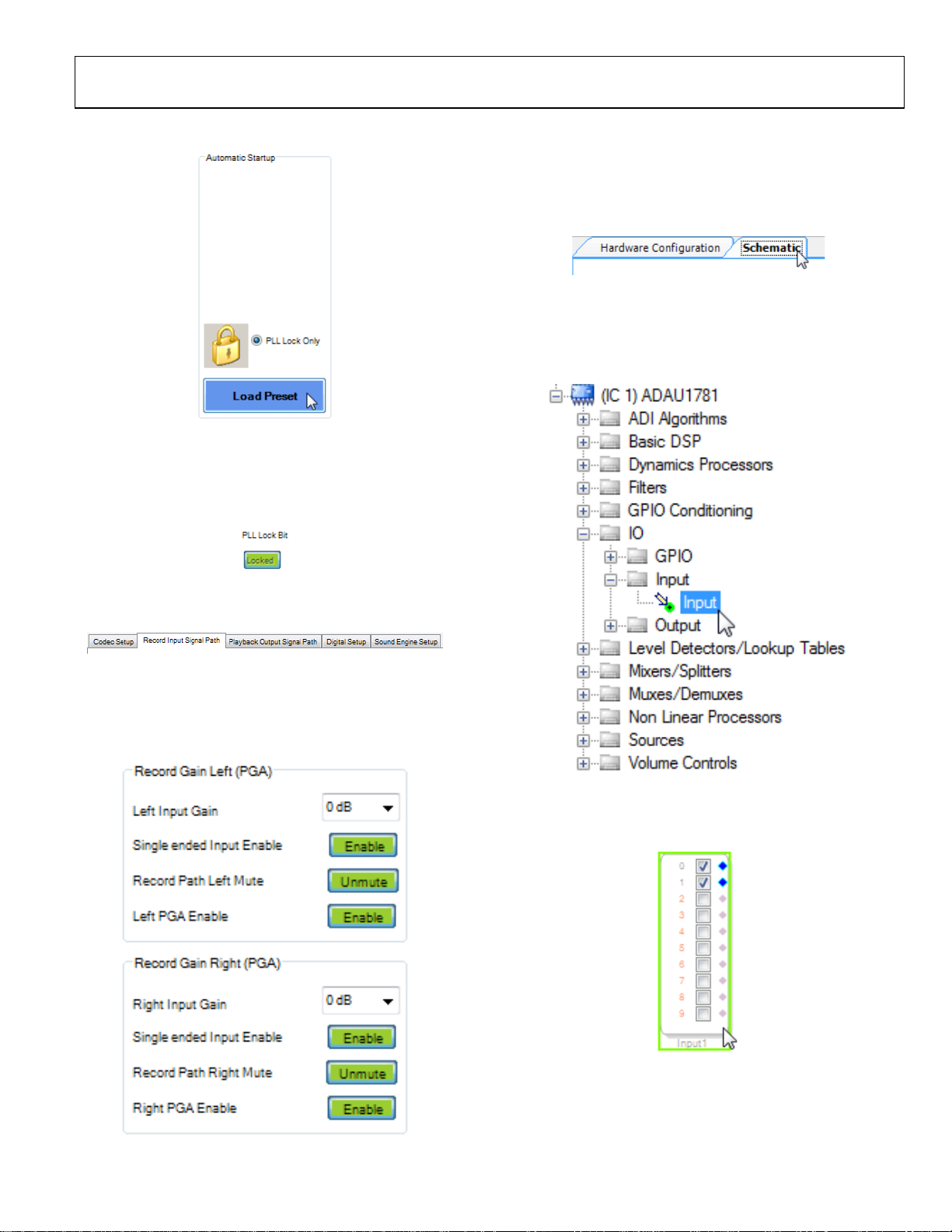
In the Automatic Startup section, click Load Preset (see Figure 17).
08314-017
Figure 17. Load Preset Button
If the board is connected and powered and the USBi drivers are
installed correctly, the PLL Lock Bit indicator to the left of the
Load Preset button should change to green to indicate that it is
Locked (see Figure 18).
The rest of the register settings can remain at their default values.
CREATING A BASIC SIGNAL FLOW
To acc es s the Schematic tab, where a signal processing flow
can be created, click the Schematic tab at the top of the screen
(see Figure 21).
8314-021
Figure 21. Schematic Tab
The left side of the schematic view includes the Tree Tool box,
which contains all of the algorithms that can run in the
SigmaDSP. Select the Input cell from within the IO > Input
folder (see Figure 22).
08314-018
Figure 18. PLL Lock Indicator
Click on the Record Input Signal Path tab (see Figure 19).
Figure 19. Record Input Signal Path
In the Record Gain Left (PGA) and Record Gain Right (PGA)
sections, the Single ended Input Enable controls are disabled by
default. Click each button once to enable the single-ended input
(see Figure 20).
08314-01
08314-022
Figure 22. Input Cell Selection
Click and drag the Input cell into the blank schematic space to
the right of the Tree Toolb ox (see Figure 23).
8314-023
Figure 23. Input Cell
8314-020
Figure 20. Record Path Controls
Rev. 0 | Page 7 of 24
UG-177 Evaluation Board User Guide
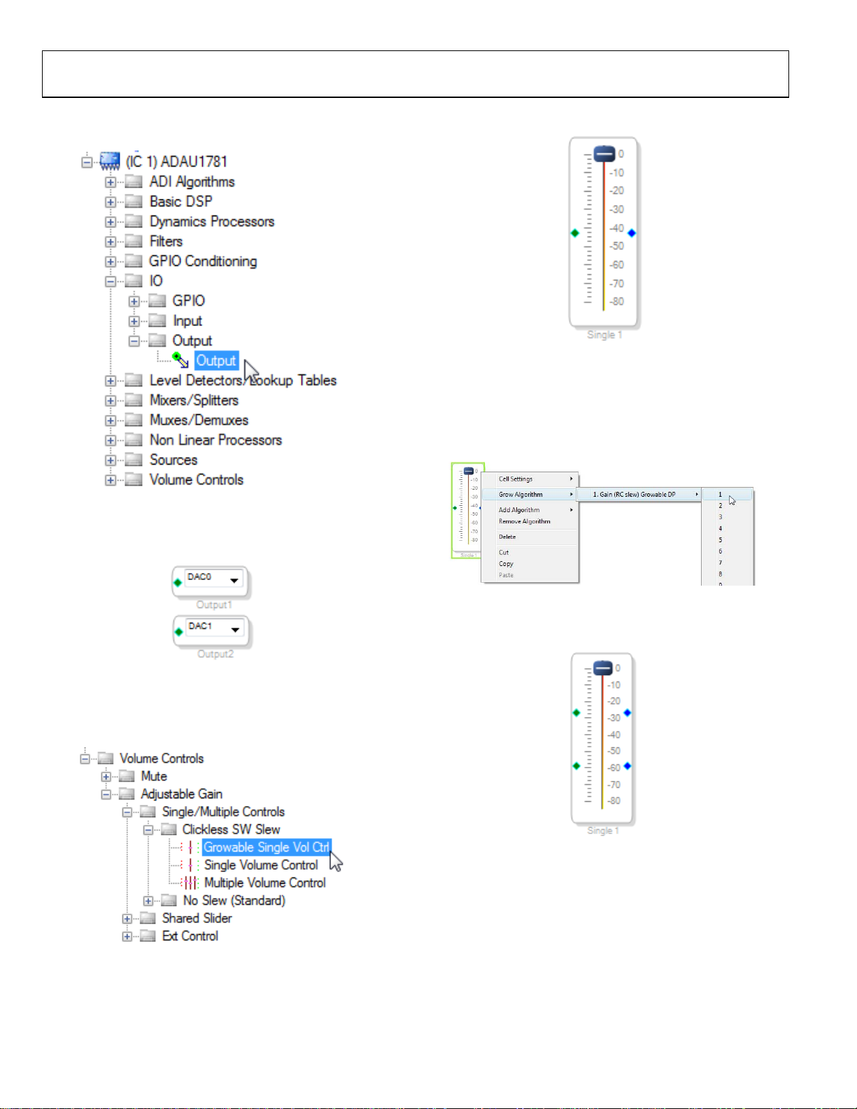
Navigate to the IO > Output folder and select the Output cell
(see Figure 24).
8314-024
Figure 24. Output Cell Selection
Click and drag an output cell to the schematic. Do this again to
create two outputs (see Figure 25).
Click and drag this cell to the schematic (see Figure 27).
Figure 27. Volume Control Cell
08314-027
By default, this cell only has one input channel and one output
channel, as indicated by the green input and right output dots.
To add a channel, right-click in the blank white part of the cell
and select Grow Algorithm > 1. Gain (RC slew) Growable DP > 1
from the menu (see Figure 28).
08314-025
Figure 25. Output Cells
Navigate to the Volume Controls > Adjustable Gain > Single/
Multiple Controls/Clickless SW Slew folder and select the
Growable Single Vol Ctrl cell (see Figure 26).
8314-026
Figure 26. Volume Control Cell Selection
Figure 28. Growing the Volume Control
The cell should now have two inputs and two outputs (see
Figure 29).
08314-029
Figure 29. Stereo Volume Control Cell
8314-028
Rev. 0 | Page 8 of 24

Evaluation Board User Guide UG-177
Navigate to the Filters > Second Order > Single Precision >
Optimized > 2 Ch folder and select the Medium Size Eq cell
(see Figure 30).
08314-030
Figure 30. EQ Cell Selection
Click and drag the cell to the schematic (see Figure 31).
The EQ should now have five bands (see Figure 33).
08314-033
Figure 33. Five-Band Stereo EQ Cell
To change the properties of a filter. Click its corresponding blue
filter icon once (see Figure 34).
8314-034
Figure 34. Filter Properties Button
Configure each filter as required. As an example, create a low
shelf at 50 Hz, peaking filters at 200 Hz, 500 Hz, and 2000 Hz,
and a high shelf at 10 kHz (see Figure 35).
8314-031
Figure 31. Single-Band Stereo EQ Cell
By default, the EQ only has one band. To increase the number
of bands, right click in the blank white part of the cell and select
Grow Algorithm > 1. 2 Channel - Single Precision, Optimized > 4
to increase the EQ to 5 bands (see Figure 32).
Figure 32. Growing the EQ Cell
Rev. 0 | Page 9 of 24
08314-035
Figure 35. Configured Five-Band EQ Cell
08314-032

UG-177 Evaluation Board User Guide
Connect the cells together by left-clicking a blue output dot and
clicking and dragging to the green output dot of the next cell.
Continue until the signal flow is completed from input to
output for each channel (see Figure 36).
Figure 36. Completed Signal Flow
The basic signal flow is now complete with stereo I/O, a fiveband equalizer, and a clickless volume control.
08314-036
DOWNLOADING THE PROGRAM TO THE DSP
To compile and download the code to the DSP, click LinkCompile-Download once in the main toolbar of SigmaStudio
(see Figure 37). Alternately, press the F7 key.
08314-037
Figure 37. Link-Compile-Download Button
The signal flow should now be running on the evaluation board,
and audio should pass from input to output. The controls for
filters and volume can be changed in real time by clicking and
dragging them with the mouse.
Rev. 0 | Page 10 of 24

Evaluation Board User Guide UG-177
USING THE EVALUATION BOARD
POWER
Power can be supplied via the USB bus by connecting the
EVAL-ADUSB2EBZ (USBi) to Header J2, by a battery connected
to J15, or by a tip-positive 3.8 V dc to 6 V dc power supply on
Connector J16. In the case of power over the USB bus, connect
Jumper J1. The on-board regulator generates the 3.3 V dc supply
for the on-board circuitry. LED D1 lights up when power is
supplied to the board. To connect the output of the regulator
to the ADAU1781, connect the J10 and J11 jumpers. Optionally,
J9 can be connected if the speaker outputs are used.
MASTER CLOCK
The master clock to the ADAU1781 can be supplied either by
an on-board active 12.288 MHz oscillator or over the serial port
connectors. Setting the MCKI source selector switch to the OSC
position connects the active oscillator to the master clock input
pin of the ADAU1781. Setting this switch to the I
connects the master clock input of the ADAU1781 to Pin 3 on
Serial Audio Interface Header J4, which is labeled MCKI.
2
S position
INPUTS AND OUTPUTS
The board has multiple audio input and output options, including
digital and analog. The analog beep channel is always enabled.
The input select switch, S4, chooses among the remaining audio
input options: stereo line input, digital microphones, and analog
microphones.
Stereo Line Input
The stereo input jack, J19, accepts a standard stereo TRS 1/8-inch
mini-plug with two channels of audio.
Digital Microphones
Digital microphones can be connected to Header J12.
Analog Microphones
Two ADMP401 MEMS analog microphones in a single-ended
configuration are mounted on the underside of the board. External
analog microphones, in both differential and single-ended input
configurations, can be connected to the input jacks, J20 and J21.
If plugs are connected into the J20 and J21 jacks, the on-board
MEMS microphones are automatically disconnected. A bias
should be applied to external differential microphones by
connecting the J13 and J14 jumpers.
Beep Input
The analog beep input accepts a mono TS 1/8-inch mini-plug
with one channel of audio.
Headphone Output
The headphone output connects to any standard 1/8-inch miniplug stereo headphones. The output power varies depending on
the impedance of the headphones.
Speaker Outputs
To use the speaker output, SVDD Power Jumper J9 must be
connected. The speaker output of the ADAU1781 can drive an
external speaker or an on-board speaker. In the case of an external
speaker, it should be connected to the Speaker Output Connector J8
and the J5 and J6 jumpers should be disconnected. To use the
on-board speaker, disconnect J8 and connect J5 and J6.
GPIO
The GPIO jumper header J7 allows the GPIO circuitry, consisting
of switches and LEDs, to be connected to the GPIO pins of
the ADAU1781. If the GPIO circuitry is connected, then the
corresponding pins cannot be used for the serial audio interface.
SERIAL AUDIO INTERFACE
Serial audio signals in I2S or TDM format can be connected to
the Serial Audio Interface Header J4. This header also includes
master clock input and output connection pins.
COMMUNICATIONS HEADER
The Communications Header J1 connects to the EVALADUSB2EBZ. More information about the USBi can be found
in the AN-1006 application note.
2
The ADAU1781 uses I
An SPI can be used by moving several resistors on the bottom
side of the board. To use SPI mode, move Resistor R35 to the
R36 pads, move Resistor R37 to the R38 pads, move Resistor
R39 to the R41 pads, and move Resistor R43 to the R42 pads.
C communications protocol by default.
POWER-DOWN
The Power-Down Header J3, labeled \PDN on the silkscreen
of the board, provides access to the power-down pin on the
ADAU1781. On this 3-pin header, a 2-pin jumper can be used
to connect the power-down pin to either the USBi or to ground.
Rev. 0 | Page 11 of 24

UG-177 Evaluation Board User Guide
MICBIAS
EVALUATION BOARD SCHEMATICS AND ARTWORK
J18
RING
SLEEVE
Speaker Out
SP1
+
1-2
J5
J6
8OHM_SPEAKER_PROJUNL_1508MS
47uF
C40
C4
+
TP5
J9
3V3DD
J11
TP9
AVDD
TP7
3V3DD
J10
IOVDD
TP6
+
10uF
C39
0.10uF
10uF
C7
C5
+
0.10uF
+
C310uF
C6
0.10uF
DVDD_OUT
0.10uF
C2
J8
2
1
SPRING_2TERM_LEVER_TH
R16
C11
10k0
100pF
10k0
TP11
19
4
5
12
32
C31
0.10uF
MICBIAS
Input
Select
Switch
TIP
Stereo Single-Ended Output
R57
10k0
R53
10k0
C19
220uF
+
R19
10R0
1
O
AD8397ARDZ
U2-A
C8
+
2-3
R14
22
20
SPP
SPN
AVDD2
AVDD
DVDDOUT
IOVDD
MIC_BIAS
3
S4-A
124
C18
220uF
+
10R0
R18
7
Stereo HP Amplifier
O
U2-B
100pF
26
AOUTL
RMIC/RMICN/MICD228RMICP29LMICP30LMIC/L MICN/MICD1
27
AD8397ARDZ
+
R15
10k0
6-5
10k0
R13
BCLK
LRCLK
ADC_SDATA
TP10
25
AOUTR
U1
ADAU1381B_QFN
DAC_SDATA
49R9
49R9
GPIO
R9 49R9
R11
R10
16
7
13
15
GPIO
BCLK
LRCLK
DAC_SDATA14ADC_SDATA
SDA/COUT10ADDR0/CDATA
SCL/CCLK
ADDR1/CLATCH
PDN
BEEP
2
PDN
7
9
31
568
8
11
17
SCL/CCLK
SDA/COUT
ADDR0/CDATA
ADDR1/CLATCH
S4-B
MCKI18MCKO
08314-038
3V3DD
L1
12
C36
0.10uF
1
12.288MHz
VDD
OE
GND
2
4
U4
3
C14
10uF
EXT_MCLK
OUTPUT
COMPANY:
+
R45
C9
0.10uF
R48
1
CM
AGND2
23
AGND
3
DGND
6
THERM_PAD
33
49R9
R12
MCKO
49R9
49R9
C38
2.2pF
6
123
4
S3
5
DPDT_SLIDE_VERT_EG2207
R52
MICD1
Stereo Digital Mic Input
C25
10uF
C29
R32
49k9
R31
0R00
J14
R34
2k00
C30
0.10uF
STX-3150-5C
Differential Input 1
C24
OPEN
J21
10uF
C28
OPEN
C20
R30
49k9
R26
0R00
M2
1
GND
3
5
GND
OUTPUT
2
VDD
GND
4
Analog Mic 1
3V3DD
ADMP401A_MEMS_MIC
C49
0.10uF
10uF
C21
OPEN
R24
49k9
R23
1k00
TIP
RING
SLEEVE
J19
Stereo Single-Ended Input
10k0
C16
10uF
C17
OPEN
R22
49k9
R21
1k00
MICBIAS
C23
10uF
C27
R29
R28
0R00
J13
R33
2k00
C12
0.10uF
STX-3150-5C
C22
10uF
C26
OPEN
49k9
J20
OPEN
R27
49k9
R25
0R00
M1
1
GND
3
5
GND
OUTPUT
2
VDD
GND
Analog Mic 2
3V3DD
4
C47
0.10uF
C15
10uF
49k9
R20
TIPJ17
RING
SLEEVE
ADMP401A_MEMS_MIC
BEEP input
Differential Input 2
Figure 38. Evaluation Board Schematic—SigmaDSP, Analog I/O, and Master Clock Generation
Rev. 0 | Page 12 of 24

Evaluation Board User Guide UG-177
8314-039
Figure 39. Evaluation Board Schematic—Digital Microphone Interface
08314-040
Figure 40. Evaluation Board Schematic—Serial Audio Data Interface
08314-041
Figure 41. Evaluation Board Schematic—Power Supply
Rev. 0 | Page 13 of 24

UG-177 Evaluation Board User Guide
08314-042
Figure 42. Evaluation Board Schematic—GPIO Interface
8314-043
Figure 43. Evaluation Board Schematic—Communications Interface
Rev. 0 | Page 14 of 24

Evaluation Board User Guide UG-177
Figure 44. Evaluation Board Layout—Top Assembly
Rev. 0 | Page 15 of 24
8314-044

UG-177 Evaluation Board User Guide
Figure 45. Evaluation Board Layout—Top Copper
Rev. 0 | Page 16 of 24
08314-045

Evaluation Board User Guide UG-177
Figure 46. Evaluation Board Layout—Power Plane
Rev. 0 | Page 17 of 24
08314-046

UG-177 Evaluation Board User Guide
Figure 47. Evaluation Board Layout—Ground Plane
Rev. 0 | Page 18 of 24
08314-047

Evaluation Board User Guide UG-177
Figure 48. Evaluation Board Layout—Bottom Copper
Rev. 0 | Page 19 of 24
08314-048

UG-177 Evaluation Board User Guide
08314-049
Figure 49. Evaluation Board Layout—Bottom Assembly
Rev. 0 | Page 20 of 24

Evaluation Board User Guide UG-177
ORDERING INFORMATION
BILL OF MATERIALS
Table 1.
Qty. Designator Description Value Manufacturer Part Number
19
C1, C2, C4 to C6,
C9, C12, C30, C31,
C33, C35 to C37,
C41 to C44,
C47, C49
7
C3, C7, C14, C32,
C34, C39, C45
2 C8, C11
7
C10, C17, C21,
C26 to C29
3 C13, C46, C48
7
C15, C16, C20,
C22 to C25
2 C18, C19
1 C38
1 C40 Tantalum capacitor, 105°C SMD 47 μF Kemet T520B476M010ATE035
1 C50
16
R1, R2, R13 to R17,
R39, R43, R46, R47,
R52 to R55, R57
4 R3, R4, R7, R8
11
R5, R6, R9 to R12,
R45, R48, R50,
R51, R56
2 R18, R19
7
R20, R22, R24, R27,
R29, R30, R32
2 R21, R23
6
R25, R26, R28, R31,
R35, R37
2 R33, R34
7
R36, R38, R40 to
R42, R44, R49
1 SP1
1 U1
1 U2
1 U3
Multilayer ceramic, 16 V,
X7R (0402)
SMD tantalum capacitor,
0805, 6.3 V
Multilayer ceramic, 50 V,
NP0 (0402)
Do not insert Open Do not insert Do not insert
Multilayer ceramic, 16 V,
X7R (0603)
Multilayer ceramic, 10 V,
X7R (0805)
SMD tantalum capacitor,
SMD, 6.3 V
Multilayer ceramic, 50 V,
NP0 (0402)
Multilayer ceramic, 25 V,
NP0 (0603)
Chip resistor, 1%, 63 mW,
thick film, 0402
Chip resistor, 1%, 63 mW,
thick film, 0402
Chip resistor, 1%, 63 mW,
thick film, 0402
Chip resistor, 1%, 125 mW,
thick film, 0805
Chip resistor, 1%, 63 mW,
thick film, 0402
Chip resistor, 1%, 0.1 W,
thick film, 0402
Chip resistor, 0.1 W,
thick film, 0402
Chip resistor, 1%, 0.1 W,
thick film, 0402
Do not insert Open Do not insert Do not insert
Speaker, 8 Ω, 0.5 W, 87 dB,
15 mm, SMD
4 ADC, 4 DAC with PLL,
24-bit codec
Rail-to-rail, high output
current amplifier
High accuracy low dropout
3.3 V dc voltage regulator
0.10 μF Panasonic EC ECJ-0EX1C104K
10 μF Rohm Semiconductor TCP0J106M8R
100 pF Murata ENA GCM1555C1H101JZ13D
1.0 μF Taiyo Yuden EMK107BJ105KA-TR
10 μF Murata ENA GRM21BR71A106KE51L
220 μF Nichicon F930J227MNC
2.2 pF Johanson Tech. 500R07S2R2BV4T
10 nF TDK Corp. C1608C0G1E103J
10 kΩ Rohm Semiconductor MCR01MZPF1002
301 Ω Rohm Semiconductor MCR01MZPF3010
49.9 Ω Rohm Semiconductor MCR01MZPF49R9
10 Ω Panasonic EC ERJ-6ENF10R0V
49.9 kΩ Vishay/Dale CRCW040249K9FKED
1 kΩ Panasonic EC ERJ-2RKF1001X
0 Ω Panasonic EC ERJ-2GE0R00X
2 kΩ Panasonic EC ERJ-2RKF2001X
8 Ω PC mount Projects Unlimited SMS-1508MS-R
ADAU1781 Analog Devices ADAU1781
AD8397ARDZ Analog Devices, Inc. AD8397ARDZ
ADP3339AKCZ-3.3-R7 Analog Devices ADP3339AKCZ-3.3-R7
Rev. 0 | Page 21 of 24

UG-177 Evaluation Board User Guide
Qty. Designator Description Value Manufacturer Part Number
1 U4
2 U5, U6
1 U7
2 M1, M2
2 S1, S2
1 S3 DPDT slide switch vertical DPDT slide E-Switch EG2207
1 S4
1 L1 Chip ferrite bead 600 Ω at 100 MHz TDK Corp. MMZ1005S601C
8
J1, J5, J6, J9 to J11,
J13, J14
1 J2
1 J3 3-position SIP header 3-pin jumper
1 J4 Header, 12-way, unshrouded 2 × 6
1 J7 Header, 10-way, unshrouded 2 × 5
1 J8
1 J12 12-way socket unshrouded 2 × 6
1 J15 2-pin header R/A, 100 mil gold 22-12-2-24 Molex 22-12-2024
1 J16 Power supply connector RAPC722X Switchcraft, Inc. RAPC722X
3 J17 to J19 Sterero mini-jack SJ-3523-SMT CUI Inc. SJ-3523-SMT
2 J20, J21
2 D1, D4
1 D2
1 D3
3 D5 to D7
13 TP1 to TP13 Mini-test point, white, 0.1" OD 5002 Keystone Electronics 5002
12.288 fixed SMD oscillator,
1.8 V dc to 3.3 V dc
Translator 1-bit, unidirect,
SC70-5
Adjustable low dropout
voltage regulator
Omnidirectional microphone
with bottom port and
analog output
Tact switch long stroke
(normally open)
Switch slide, DP3T,
PC mount, L = 4 mm
2-pin header unshrouded
jumper, 0.10", use shunt
Tyco 881545-2
10-way shroud polarized
header
2-position spring terminal
block
Sterero mini-jack with tip
and ring normal
Red diffused, 6.0 millicandela,
635 nm, 1206
Green diffused, 10 millicandela,
565 nm, 1206
Yellow diffused, 4.0 millicandela,
585 nm, 1206
Schottky, 30 V, 0.5 A,
SOD123 diode
12.288 MHz Abracon Corp. AP3S-12.288MHz-F-J-B
FXLP34P5X Fairchild Semiconductor FXLP34P5X
ADP1711AUJZ-1.8-R7 Analog Devices ADP1711AUJZ-1.8-R7
ADMP401-1 Analog Devices ADMP401-1
70 gf Omron Electronics B3M-6009
2P3T slide E-Switch EG2305
2-pin jumper
2 × 5 3M N2510-6002RB
14-30 AWG spring clamp On-Shore Tech. OSTHT020080
STX-3150-5C Kycon STX-3150-5C
Red diffused Lumex Opto SML-LX1206IW-TR
Green diffused Lumex Opto SML-LX1206GW-TR
Yellow diffused CML Innovative Tech CMD15-21VYD/TR8
Schottky ON Semiconductor MBR0530T1G
Sullins Connector
Solutions
Sullins Connector
Solutions
Sullins Connector
Solutions
Sullins Connector
Solutions
Sullins Connector
Solutions
PBC02SAAN or
cut PBC36SAAN
PBC03SAAN or
cut PBC36SAAN
PBC06DAAN
PBC05DAAN
PPPC062LFBN-RC
RELATED LINKS
Resource Description
ADAU1781 Product Page, SigmaDSP Low-noise Stereo Audio Codec for Portable Applications
ADMP401 Product Page, Omnidirectional Microphone with Bottom Port and Analog Output
AN-1006 Application Note, Using the EVAL-ADUSB2EBZ
Rev. 0 | Page 22 of 24

Evaluation Board User Guide UG-177
NOTES
Rev. 0 | Page 23 of 24

UG-177 Evaluation Board User Guide
NOTES
I2C refers to a communications protocol originally developed by Philips Semiconductors (now NXP Semiconductors).
ESD Caution
ESD (electrostatic discharge) sensitive device. Charged devices and circuit boards can discharge without detection. Although this product features patented or proprietary protection
circuitry, damage may occur on devices subjected to high energy ESD. Therefore, proper ESD precautions should be taken to avoid performance degradation or loss of functionality.
Legal Terms and Conditions
By using the evaluation board discussed herein (together with any tools, components documentation or support materials, the “Evaluation Board”), you are agreeing to be bound by the terms and conditions
set forth below (“Agreement”) unless you have purchased the Evaluation Board, in which case the Analog Devices Standard Terms and Conditions of Sale shall govern. Do not use the Evaluation Board until you
have read and agreed to the Agreement. Your use of the Evaluation Board shall signify your acceptance of the Agreement. This Agreement is made by and between you (“Customer”) and Analog Devices, Inc.
(“ADI”), with its principal place of business at One Technology Way, Norwood, MA 02062, USA. Subject to the terms and conditions of the Agreement, ADI hereby grants to Customer a free, limited, personal,
temporary, non-exclusive, non-sublicensable, non-transferable license to use the Evaluation Board FOR EVALUATION PURPOSES ONLY. Customer understands and agrees that the Evaluation Board is provided
for the sole and exclusive purpose referenced above, and agrees not to use the Evaluation Board for any other purpose. Furthermore, the license granted is expressly made subject to the following additional
limitations: Customer shall not (i) rent, lease, display, sell, transfer, assign, sublicense, or distribute the Evaluation Board; and (ii) permit any Third Party to access the Evaluation Board. As used herein, the term
“Third Party” includes any entity other than ADI, Customer, their employees, affiliates and in-house consultants. The Evaluation Board is NOT sold to Customer; all rights not expressly granted herein, including
ownership of the Evaluation Board, are reserved by ADI. CONFIDENTIALITY. This Agreement and the Evaluation Board shall all be considered the confidential and proprietary information of ADI. Customer may
not disclose or transfer any portion of the Evaluation Board to any other party for any reason. Upon discontinuation of use of the Evaluation Board or termination of this Agreement, Customer agrees to
promptly return the Evaluation Board to ADI. ADDITIONAL RESTRICTIONS. Customer may not disassemble, decompile or reverse engineer chips on the Evaluation Board. Customer shall inform ADI of any
occurred damages or any modifications or alterations it makes to the Evaluation Board, including but not limited to soldering or any other activity that affects the material content of the Evaluation Board.
Modifications to the Evaluation Board must comply with applicable law, including but not limited to the RoHS Directive. TERMINATION. ADI may terminate this Agreement at any time upon giving written notice
to Customer. Customer agrees to return to ADI the Evaluation Board at that time. LIMITATION OF LIABILITY. THE EVALUATION BOARD PROVIDED HEREUNDER IS PROVIDED “AS IS” AND ADI MAKES NO
WARRANTIES OR REPRESENTATIONS OF ANY KIND WITH RESPECT TO IT. ADI SPECIFICALLY DISCLAIMS ANY REPRESENTATIONS, ENDORSEMENTS, GUARANTEES, OR WARRANTIES, EXPRESS OR IMPLIED, RELATED
TO THE EVALUATION BOARD INCLUDING, BUT NOT LIMITED TO, THE IMPLIED WARRANTY OF MERCHANTABILITY, TITLE, FITNESS FOR A PARTICULAR PURPOSE OR NONINFRINGEMENT OF INTELLECTUAL
PROPERTY RIGHTS. IN NO EVENT WILL ADI AND ITS LICENSORS BE LIABLE FOR ANY INCIDENTAL, SPECIAL, INDIRECT, OR CONSEQUENTIAL DAMAGES RESULTING FROM CUSTOMER’S POSSESSION OR USE OF
THE EVALUATION BOARD, INCLUDING BUT NOT LIMITED TO LOST PROFITS, DELAY COSTS, LABOR COSTS OR LOSS OF GOODWILL. ADI’S TOTAL LIABILITY FROM ANY AND ALL CAUSES SHALL BE LIMITED TO THE
AMOUNT OF ONE HUNDRED US DOLLARS ($100.00). EXPORT. Customer agrees that it will not directly or indirectly export the Evaluation Board to another country, and that it will comply with all applicable
United States federal laws and regulations relating to exports. GOVERNING LAW. This Agreement shall be governed by and construed in accordance with the substantive laws of the Commonwealth of
Massachusetts (excluding conflict of law rules). Any legal action regarding this Agreement will be heard in the state or federal courts having jurisdiction in Suffolk County, Massachusetts, and Customer hereby
submits to the pers onal jurisdiction and venu e of such courts. The United Nations Conventi on on Contracts for the Internation al Sale of Goods shall not apply to this Agreement and is expressly disclaimed.
©2010 Analog Devices, Inc. All rights reserved. Trademarks and
registered trademarks are the property of their respective owners.
UG08314-0-7/10(0)
Rev. 0 | Page 24 of 24
 Loading...