Evaluation Board User Guide
UG-107
One Technology Way • P. O . Box 9106 • Norwood, MA 02062-9106, U.S.A. • Tel : 781.329.4700 • Fax : 781.461.3113 • www.analog.com
Evaluation Board for Dual High Speed Selectable Gain Differential Amplifiers
(24-Lead, 4 mm × 4 mm LFCSP)
FEATURES
Enables quick breadboarding/prototyping
Selectable gain of 1, 2, or 3
Edge-mounted SMA connector provisions
Easy connection to test equipment and other circuits
Two independent circuits enhance flexibility
GENERAL DESCRIPTION
The EB-D24CP44SG-2Z is designed to aid in the evaluation
of dual high speed, selectable gain differential amplifiers. It
has the flexibility to choose between the gain of 1, 2, or 3.
The EB-D24CP44SG-2Z is a bare board (that is, there are
no components soldered to the board) that enables users to
quickly prototype a variety of differential amplifier circuits,
which minimizes risk and reduces time to market. The
EB-D24CP44SG-2Z evaluation board supports any of
Analog Devices, Inc., dual high speed differential amplifiers
in 4 mm × 4 mm lead frame chip scale packages (LFCSP).
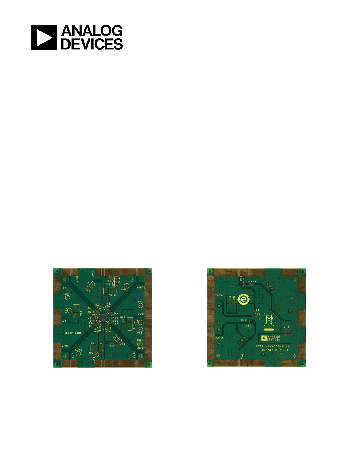
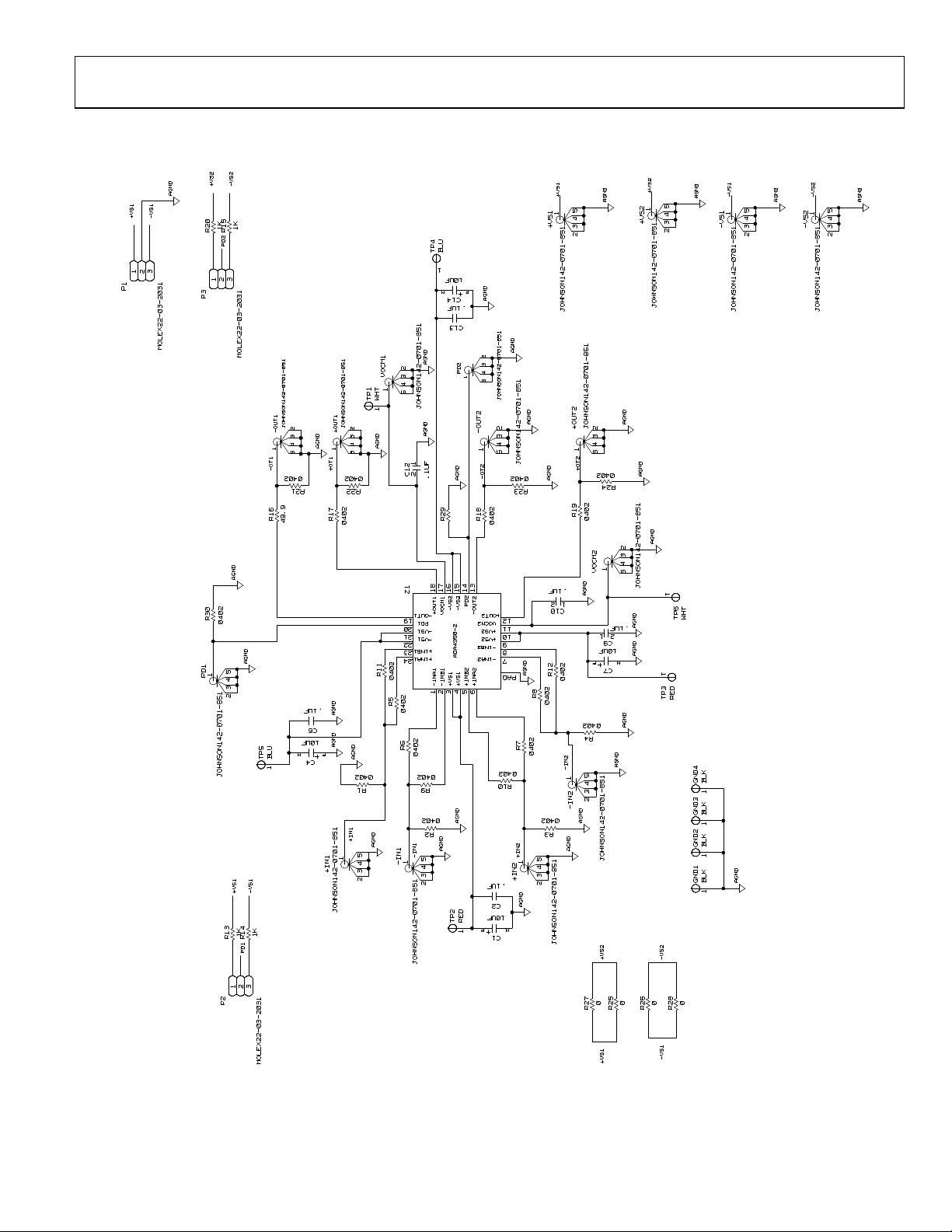
Figure 1 and Figure 2 show the component side and circuit side
of the evaluation board. Figure 3 shows the evaluation board
schematic.
The 4-layer evaluation board accepts edge-mounted SMA connectors on both inputs and outputs, which allows efficient and
quick connection to test equipment or other circuitry.
The board ground plane, component placement, and power
supply bypassing have been optimized for maximum circuit
flexibility and performance. The evaluation board uses a variety
of SMT component case sizes: 0402, 0508, 0603, and 7343.
Figure 4 and Figure 6 show the evaluation board assembly
drawings. The metal layout pattern for connecting the board
to the op amp and to the supporting circuitry is shown in
Figure 5 and Figure 7.
NOTES
1. THE EVALUATION BOARD SILKSCREEN PART NUMBER
LABELING ON Y OUR BOARD MAY BE DIFFERENT FROM
WHAT IS SHOWN HERE.
Figure 1. Component Side of PCB Figure 2. Circuit Side of PCB
PLEASE SEE THE LAST PAGE FOR AN IMPORTANT
WARNING AND LEGAL TERMS AND CONDITIONS.
DIGITAL PICTURES OF THE EVALUATION BOARD
NOTES
1. THE EVALUATION BOARD SILKSCREEN PART NUMBER
LABELING ON YOUR BOARD MAY BE DIFFERENT FRO M
08894-001
Rev. 0 | Page 1 of 8
WHAT IS SHOWN HERE.
08894-007

UG-107 Evaluation Board User Guide
TABLE OF CONTENTS
Features .............................................................................................. 1
General Description ......................................................................... 1
Digital Pictures of the Evaluation Board ....................................... 1
REVISION HISTORY
4/10—Revision 0: Initial Version
Revision History ................................................................................2
Evaluation Board Schematic ............................................................3
Assembly Drawing and Board Layout ............................................4
Rev. 0 | Page 2 of 8

Evaluation Board User Guide UG-107
EVALUATION BOARD SCHEMATIC
-VS2
+VS2
AGND
+VS1
-VS1
1
3
2
P1
MOLEX22-03-2031
1K
1K
R20
R15
PD2
1
3
2
P3
MOLEX22-03-2031
TP1
*
0402
R21
NP
JOHNSON142-0701-851
+OUT1
AGND
1
5432
+OT1
*
0402
R22
R17
040
*
.1UF
C6
10UF
AGND AGND
AGND
C4
04
R1
+IN1
5432
1
JOHNSON142-0701-851
-OUT1
1
5432
-OT1
R16
49.9
AGND
R30
040
*
AGND
5432
1
PD1
TP5
BLU
JOHNSON142-0701-851
1
+IN1
-VS1
+VS1
JOHNSON142-0701-851
1K
1K
R13
R14
PD1
1
3
2
P2
08894-002
*
JOHNSON142-0701-851
+VS2+VS1
AGND
1
*
0402
R24
2
C9
10UF
NP
C7
AGND
R25
5432
0
AGND
AGND
AGND
AGND
+VS2
5432
1
+VS2
JOHNSON142-0701-851
AGND
AGND
JOHNSON142-0701-851
1
TP6
AGND
-VS1
5432
1
-VS1
JOHNSON142-0701-851
AGND
-VS2
1
AGND
5432
-VS2
JOHNSON142-0701-851
WHT
USER-DEFINED VALUES
*
1
TP3
RED
GND4
BLK
1
GND3
1
GND2
BLK
1
GND1
BLK BLK
AGND
1
-VS2
0
0
R28
R26
+VS1
5432
1
+VS1
TP4
BLU
1
10UF
NP
C14
AGND
WHT
1
AGND
VOCM1
1
AGND
5432
JOHNSON142-0701-851
AGND
1
C12
2
.1UF
.1UF
C13
AGND
PD2
1
5432
JOHNSON142-0701-851
-OUT2
1
5432
-OT2
AGND
R18
R29
040
*
JOHNSON142-0701-851
AGND
JOHNSON142-0701-851
*
0402
R23
JOHNSON142-0701-851
+OUT2
1
5432
+OT2
AGND
R19
040
*
VOCM2
R7
*
+IN2
.1UF
AGND
2
1
C10
1
AGND
R12
040
*
R8
040
*
0402
040
*
5432
1
AGND
R4
-IN2
5432
1
-IN2
*
04
AGND
R3
AGND
JOHNSON142-0701-851
Z1
19
20
21
22
23
24
R11
040
*
40
R5
0
*
R6
040
*
*
2
2
AGND
-IN1
1
-IN1
PD2
-VS2
-VS2
VOCM1
-OUT2
+OUT1
-OUT1
PD1
-VS1
-VS1
+1NB1
+1NA1
+VS1
-1NB1
-1NA1
1
3
2
*
0402
R9
*
04
R2
AGND
5432
+OUT2
12
VOCM2
11
+VS2
10
+VS2
9
-1NB2
ADA4950-2
AGND
TP2
8
-1NA2
7
+1NB2
+VS1
RED
1
PAD
+1NA2
654
0402
2
R10
+IN2
.1UF
C2
10UF
NP
C1
14
13
15
16
18
17
JOHNSON142-0701-851
0
R27
MOLEX22-03-2031
-VS1
Figure 3. Dual Differential Amplifier Universal Evaluation Board Schematic
Rev. 0 | Page 3 of 8

UG-107 Evaluation Board User Guide
ASSEMBLY DRAWING AND BOARD LAYOUT
Figure 4. Board Assembly Drawing, Component Side
Figure 5. Board Layout Pattern, Component Side
08894-003
Figure 6. Board Assembly Drawing, Circuit Side
08894-004
Figure 7. Board Layout Pattern, Circuit Side
08894-005
08894-006
Rev. 0 | Page 4 of 8

Evaluation Board User Guide UG-107
NOTES
Rev. 0 | Page 5 of 8

UG-107 Evaluation Board User Guide
NOTES
Rev. 0 | Page 6 of 8

Evaluation Board User Guide UG-107
NOTES
Rev. 0 | Page 7 of 8

UG-107 Evaluation Board User Guide
NOTES
ESD Caution
ESD (electrostatic discharge) sensitive device. Charged devices and circuit boards can discharge without detection. Although this product features patented or proprietary protection
circuitry, damage may occur on devices subjected to high energy ESD. Therefore, proper ESD precautions should be taken to avoid performance degradation or loss of functionality.
Legal Terms and Conditions
By using the evaluation board discussed herein (together with any tools, components documentation or support materials, the “Evaluation Board”), you are agreeing to be bound by the terms and conditions
set forth below (“Agreement”) unless you have purchased the Evaluation Board, in which case the Analog Devices Standard Terms and Conditions of Sale shall govern. Do not use the Evaluation Board until you
have read and agreed to the Agreement. Your use of the Evaluation Board shall signify your acceptance of the Agreement. This Agreement is made by and between you (“Customer”) and Analog Devices, Inc.
(“ADI”), with its principal place of business at One Technology Way, Norwood, MA 02062, USA. Subject to the terms and conditions of the Agreement, ADI hereby grants to Customer a free, limited, personal,
temporary, non-exclusive, non-sublicensable, non-transferable license to use the Evaluation Board FOR EVALUATION PURPOSES ONLY. Customer understands and agrees that the Evaluation Board is provided
for the sole and exclusive purpose referenced above, and agrees not to use the Evaluation Board for any other purpose. Furthermore, the license granted is expressly made subject to the following additional
limitations: Customer shall not (i) rent, lease, display, sell, transfer, assign, sublicense, or distribute the Evaluation Board; and (ii) permit any Third Party to access the Evaluation Board. As used herein, the term
“Third Party” includes any entity other than ADI, Customer, their employees, affiliates and in-house consultants. The Evaluation Board is NOT sold to Customer; all rights not expressly granted herein, including
ownership of the Evaluation Board, are reserved by ADI. CONFIDENTIALITY. This Agreement and the Evaluation Board shall all be considered the confidential and proprietary information of ADI. Customer may
not disclose or transfer any portion of the Evaluation Board to any other party for any reason. Upon discontinuation of use of the Evaluation Board or termination of this Agreement, Customer agrees to
promptly return the Evaluation Board to ADI. ADDITIONAL RESTRICTIONS. Customer may not disassemble, decompile or reverse engineer chips on the Evaluation Board. Customer shall inform ADI of any
occurred damages or any modifications or alterations it makes to the Evaluation Board, including but not limited to soldering or any other activity that affects the material content of the Evaluation Board.
Modifications to the Evaluation Board must comply with applicable law, including but not limited to the RoHS Directive. TERMINATION. ADI may terminate this Agreement at any time upon giving written notice
to Customer. Customer agrees to return to ADI the Evaluation Board at that time. LIMITATION OF LIABILITY. THE EVALUATION BOARD PROVIDED HEREUNDER IS PROVIDED “AS IS” AND ADI MAKES NO
WARRANTIES OR REPRESENTATIONS OF ANY KIND WITH RESPECT TO IT. ADI SPECIFICALLY DISCLAIMS ANY REPRESENTATIONS, ENDORSEMENTS, GUARANTEES, OR WARRANTIES, EXPRESS OR IMPLIED, RELATED
TO THE EVALUATION BOARD INCLUDING, BUT NOT LIMITED TO, THE IMPLIED WARRANTY OF MERCHANTABILITY, TITLE, FITNESS FOR A PARTICULAR PURPOSE OR NONINFRINGEMENT OF INTELLECTUAL
PROPERTY RIGHTS. IN NO EVENT WILL ADI AND ITS LICENSORS BE LIABLE FOR ANY INCIDENTAL, SPECIAL, INDIRECT, OR CONSEQUENTIAL DAMAGES RESULTING FROM CUSTOMER’S POSSESSION OR USE OF
THE EVALUATION BOARD, INCLUDING BUT NOT LIMITED TO LOST PROFITS, DELAY COSTS, LABOR COSTS OR LOSS OF GOODWILL. ADI’S TOTAL LIABILITY FROM ANY AND ALL CAUSES SHALL BE LIMITED TO THE
AMOUNT OF ONE HUNDRED US DOLLARS ($100.00). EXPORT. Customer agrees that it will not directly or indirectly export the Evaluation Board to another country, and that it will comply with all applicable
United States federal laws and regulations relating to exports. GOVERNING LAW. This Agreement shall be governed by and construed in accordance with the substantive laws of the Commonwealth of
Massachusetts (excluding conflict of law rules). Any legal action regarding this Agreement will be heard in the state or federal courts having jurisdiction in Suffolk County, Massachusetts, and Customer hereby
submits to the pers onal jurisdiction and venu e of such courts. The United Nations Conventi on on Contracts for the Internation al Sale of Goods shall not apply to this Agreement and is expressly disclaimed.
©2010 Analog Devices, Inc. All rights reserved. Trademarks and
registered trademarks are the property of their respective owners.
UG08894-0-4/10(0)
Rev. 0 | Page 8 of 8
 Loading...