Evaluation Board User Guide
UG-093
One Technology Way • P. O . Box 9106 • Norwood, MA 02062-9106, U.S.A. • Tel : 781.329.4700 • Fax : 781.461.3113 • www.analog.com
Evaluation Board for the Dual, Continuous Time Sigma-Delta Modulator
EVALUATION BOARD DESCRIPTION
The AD9267 evaluation board serves two purposes: as an
evaluation platform for the 16-bit, dual, continuous time sigmadelta (Σ-Δ) modulator and as a direct conversion demonstration
platform. Table 1 lists the product features of all the Analog
Devices, Inc., components in the demonstrator.
The AD9267 is a dual continuous time Σ-Δ modulator with
−88 dBc of dynamic range over 10 MHz real or 20 MHz
complex bandwidth. The combination of high dynamic range,
wide bandwidth, and characteristics unique to the continuous
time Σ-Δ modulator architecture makes the AD9267 an ideal
solution for wireless communication systems.
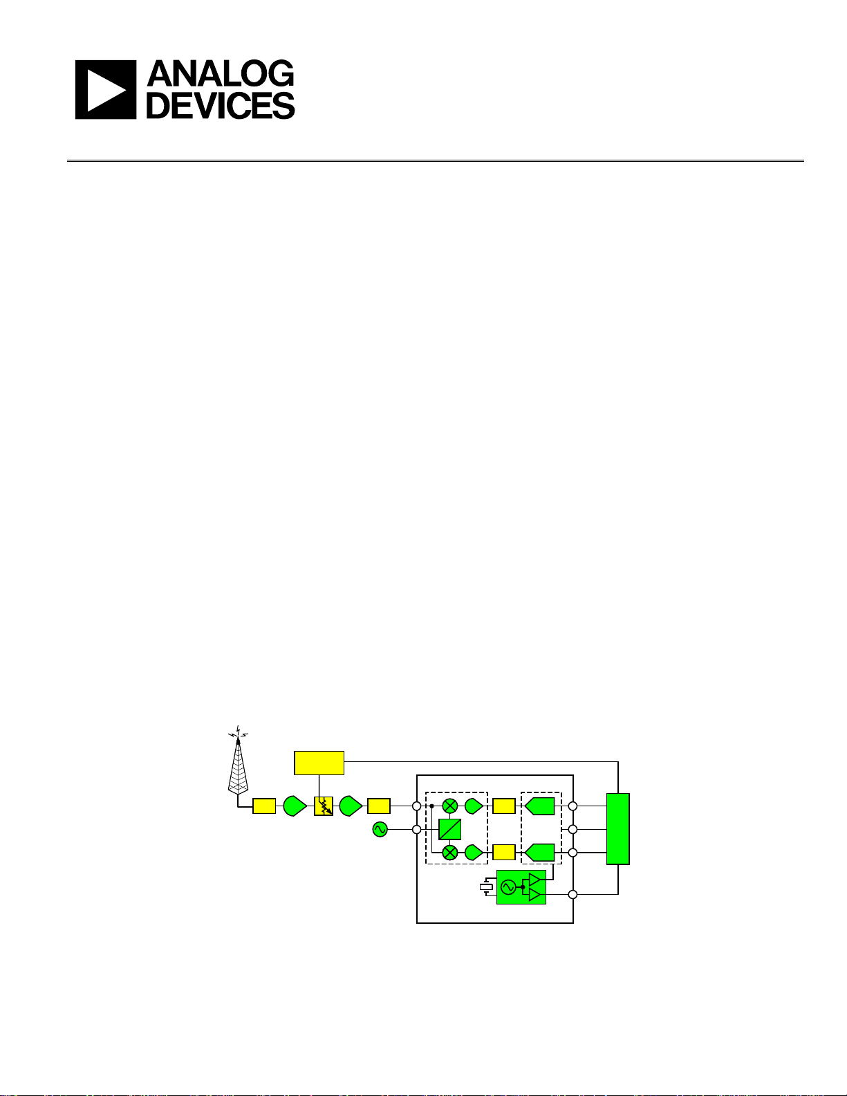
Direct conversion architectures, as shown in Figure 1, use a single
frequency translation step to convert the RF channel directly
to baseband without any intermediate frequency stages. The
frequency translation in this direct conversion demonstrator is
accomplished by the ADL5382, which is a quadrature demodulator. The ADL5382 covers the frequency range between 700 MHz
and 2.7 GHz.
The AD9267 has passive inputs, therefore allowing the ADL5382
to directly drive the modulator. The AD9267 does not require a
filter preceding the converter because the continuous time Σ-Δ
architecture possesses inherent antialiasing capabilities. Therefore,
minimal or no filtering is required between the demodulator
and the AD9267. A prototype area for a fourth-order filter is
provided in which additional filtering can be tested.
To achieve optimal performance from the AD9267, a low jitter
differential clock is necessary, and the AD9516 family of parts
offers superior clock performance. The AD9516-0 and a crystal
oscillator footprint are included on the evaluation board. In
addition to providing a clock option to the modulator, the many
outputs from the AD9516 can be used to drive other external
capture devices. AD9516 is used throughout to refer to all the
members of the AD9516 family. However, the use of AD9516-0
refers to that specific device.
The ADR130B offers the option of using an external 0.5 V band
gap reference voltage for the AD9267. The ADP3339 provides a
quiet and reliable voltage source to each of the Analog Devices
components.
In addition to offering system-level evaluation of the direct conversion architecture, the evaluation board offers the flexibility
of isolating the AD9267 from the surrounding components,
enabling a detailed evaluation of only the AD9267. The modulator
inputs can be disconnected from the ADL5382 and be driven
with an external source. The analog inputs of the AD9267 can
be driven from either a differential transformer or the ADA4937-2,
which is a very low noise, high linearity differential amplifier.
Complementing the AD9267 evaluation board are additional
hardware and software to capture and process digital data from
the output of the modulator. The AD9267 can only be evaluated
using the HSC-ADC-EVALCZ high speed ADC data capture card
in conjunction with the VisualAnalog™ data capture and analysis
software. The SPIController™ software is used to read and write
to the AD9267.
BPF
PLEASE SEE THE LAST PAGE FOR AN IMPORTANT
WARNING AND LEGAL TERMS AND CONDITIONS.
GAIN
CONTROL
ADL5523 ADL5523
BPF
ADF4360-x
Figure 1. Direct Conversion Receiver Block Diagram
Rev. 0 | Page 1 of 24
RF
LO
ADL5382
90°
0°
122.88MHz
AD9267
LPF
LPF
AD9516-0
ADC
ADC
DA
DCO
DB
DDC
8877-001
 Loading...