

Evaluation Board User Guide
One Technology Way • P. O . Box 9106 • Norwood, MA 02062-9106, U.S.A. • Tel : 781.329.4700 • Fax : 781.461.3113 • www.analog.com
UG-074
Evaluating the AD9265/AD9255 Analog-to-Digital Converters
FEATURES
Full featured evaluation board for the AD9265/AD9255
SPI interface for setup and control
External, on-board oscillator or AD9517 clocking options
Balun/transformer or amplifier input drive options
LDO regulator or switching power supply options
VisualAnalog® and SPI controller software interfaces
EQUIPMENT NEEDED
Analog signal source and antialiasing filter
Sample clock source (if not using the on-board oscillator)
2 switching power supplies (6.0 V, 2.5 A) provided, CUI, Inc.,
EPS060250UH-PHP-SZ
PC running Windows® XP or Windows Vista
USB 2.0 port recommended (USB 1.1 compatible)
AD9265 or AD9255 evaluation board
HSC-ADC-EVALCZ FPGA-based data capture kit
SOFTWARE NEEDED
VisualAnalog
SPI controller
EVALUATION BOARDS
DOCUMENTS NEEDED
AD9265 or AD9255 data sheet
HSC-ADC-EVALCZ data sheet
AN-905 Application Note, VisualAnalog Converter Evaluation
Tool Version 1.0 User Manual
AN-878 Application Note, High Speed ADC SPI Control Software
AN-877 Application Note, Interfacing to High Speed ADCs via SPI
AN-835 Application Note, Understanding High Speed ADC
Tes ti ng an d Ev al uati on
GENERAL DESCRIPTION
This user guide describes the AD9265 and AD9255 evaluation
board, which provides all of the support circuitry required to
operate the AD9265 or AD9255 in its various modes and
configurations. The application software used to interface with
the devices is also described.
The AD9265 and AD9255 data sheets provide additional
information and should be consulted when using the evaluation
board. All documents and software tools are available at
www.analog.com/fifo. For additional information or questions,
send an email to highspeed.converters@analog.com.
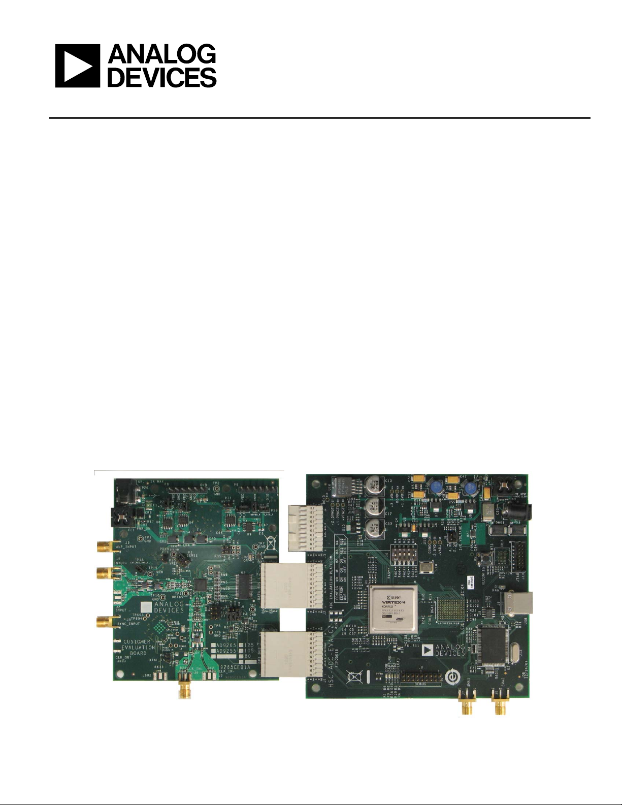
Figure 1. AD9265 and AD9255 Evaluation Board and HSC-ADC-EVALCZ Data Capture Board
Please see the last page for an important warning and disclaimers. Rev. 0 | Page 1 of 28
08699-001

UG-074 Evaluation Board User Guide
TABLE OF CONTENTS
Features .............................................................................................. 1
Equipment Needed ........................................................................... 1
Software Needed ............................................................................... 1
Documents Needed .......................................................................... 1
General Description ......................................................................... 1
Evaluation Boards ............................................................................. 1
Revision History ............................................................................... 2
Evaluation Board Hardware ............................................................ 3
Power Supplies .............................................................................. 3
REVISION HISTORY
1/11—Revision 0: Initial Version
Input Signals...................................................................................3
Output Signals ...............................................................................3
Default Operation and Jumper Selection Settings ....................5
Evaluation Board Software Quick Start Procedures .....................7
Configuring the Board .................................................................7
Using the Software for Testing .....................................................7
Evaluation Board Schematics and Artwork ................................ 11
Ordering Information .................................................................... 24
Bill of Materials ........................................................................... 24
Rev. 0 | Page 2 of 28

Evaluation Board User Guide UG-074
EVALUATION BOARD HARDWARE
The AD9265 and AD9255 evaluation board provides all of the
support circuitry required to operate these parts in their various
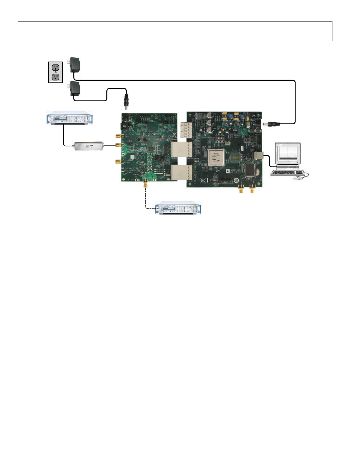
modes and configurations. Figure 2 shows the typical bench
characterization setup used to evaluate the ac performance of
the AD9265 or AD9255. It is critical that the signal sources used
for the analog input and clock have very low phase noise (<1 ps
rms jitter) to realize the optimum performance of the signal
chain. Proper filtering of the analog input signal to remove
harmonics and lower the integrated or broadband noise at the
input is necessary to achieve the specified noise performance.
See the Evaluation Board Software Quick Start Procedures section
to get started, and see Figure 15 to Figure 28 for the complete
schematics and layout diagrams. These diagrams demonstrate
the routing and grounding techniques that should be applied at
the system level when designing application boards using these
converters.
POWER SUPPLIES
This evaluation board comes with a wall-mountable switching
power supply that provides a 6 V, 2 A maximum output. Connect
the supply to the rated 100 V ac to the 240 V ac wall outlet at
47 Hz to 63 Hz. The output from the supply is provided through
a 2.1 mm inner diameter jack that connects to the printed circuit
board (PCB) at P26. The 6 V supply is fused and conditioned
on the PCB before connecting to the low dropout linear regulators
(default configuration) that supply the proper bias to each of the
various sections on the board.
The evaluation board can be powered in a nondefault condition
using external bench power supplies. To do this, the P27, P28,
P31, P30, P32, and P29 jumpers can be removed to disconnect
the outputs from the on-board LDOs. This enables the user to
bias each section of the board individually. Use P8 and P9 to
connect a different supply for each section. A 1.8 V supply is
needed with a 1 A current capability for AVDD, SVDD, and
DRVDD; however, it is recommended that separate supplies be
used for both analog and digital domains. An additional supply
is also required to supply 1.8 V for digital support circuitry on
the board, 3V_DIG. This should also have a 1 A current capability
and can be combined with DRVDD with little or no degradation in
performance.
Two additional supplies, 5V_AVDD and 3V_AVDD, are used to
bias the optional input path amplifiers. If used, these supplies
should each have a 1 A current capability. P18 is also necessary if
an amp that requires a negative supply voltage is being used.
A second optional power supply configuration allows the
replacement of the LDOs that supply the AVDD and DRVDD
rails of the ADC with the ADP2108 step-down dc-to-dc converter.
Using this switching controller in place of the LDO regulators
to power the AVDD and DRVDD supplies of the ADC allows
customers to evaluate the performance of the ADC when
powered by a more efficient regulator.
INPUT SIGNALS
When connecting the clock and analog source, use clean signal
generators with low phase noise, such as the Rohde & Schwarz
SMA100A, HP 8644B signal generators, or an equivalent. Use a
1 m shielded, RG-58, 50 Ω coaxial cable for connecting to the
evaluation board. Enter the desired frequency and amplitude (see
the Specifications section in the data sheet of the respective part).
When connecting the analog input source, use of a multipole,
narrow-band, band-pass filter with 50 Ω terminations is
recommended. Analog Devices, Inc., uses TTE and K&L
Microwave, Inc., band-pass filters. The filters should be
connected directly to the evaluation board.
If an external clock source is used, it should also be supplied
with a clean signal generator as previously specified. Typically,
most Analog Devices evaluation boards can accept ~2.8 V p-p or
13 dBm sine wave input for the clock.
OUTPUT SIGNALS
The default setup uses the Analog Devices high speed converter
evaluation platform (HSC-ADC-EVALCZ) for data capture. The
CMOS output signals are buffered through U2 and are routed
through P2 to the FPGA on the data capture board.
Rev. 0 | Page 3 of 28
UG-074 Evaluation Board User Guide
WALL OUTLET
100V AC TO 240V AC
47Hz TO 63Hz
SIGNAL
SYNTHESIZER
SWITCHING
POWER
SUPPLY
SWITCHING
POWER
SUPPLY
ANALOG INPUT
6V DC
2A MAX
SIGNAL
SYNTHESIZER
6V DC
2A MAX
PC
RUNNING ADC
ANALYZER
OR VISUAL ANALOG
USER SOFTWARE
OPTIONAL CLOCK SOURCE
08699-002
Figure 2. Evaluation Board Connection
Rev. 0 | Page 4 of 28
Evaluation Board User Guide UG-074
2
p
DEFAULT OPERATION AND JUMPER SELECTION SETTINGS
This section explains the default and optional settings or modes
allowed on the AD9265/AD9255 Rev. A evaluation board.
Power Circuitry
Connect the switching power supply that is supplied in the
evaluation kit between P26 and a rated 100 V ac to 240 V ac
wall outlet at 47 Hz to 63 Hz.
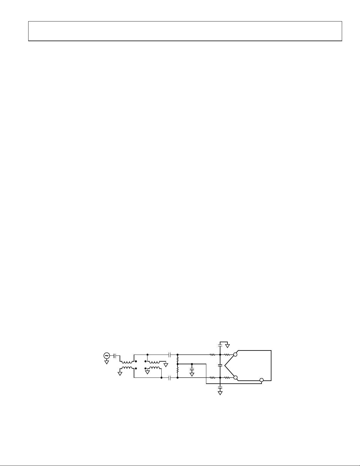
Analog Input
The inputs on the evaluation board are set up for a double baluncoupled analog input with a 50 Ω impedance. For the AD9265/
AD9255, the default analog input configuration supports analog
input frequencies of up to ~250 MHz (see Figure 3). This input
network is optimized to support a wide frequency band. See the
AD9265 and AD9255 data sheets for additional information on
the recommended networks for different input frequency ranges.
Optionally, the analog input on the board can be configured to
use the ADL5562, which is a 3.3 GHz ultralow distortion RF/IF
differential amplifier. The ADL5562 component is included on
the evaluation board at U1. However, the path into and out of the
ADL5562 can be configured in many different ways depending
on the application; therefore, the parts in the input and output
path are left unpopulated. Users should see the ADL5562 data
sheet for additional information on this part and for configuring
the inputs and outputs. The ADL5562 is normally held in powerdown mode and can be enabled by adding a jumper on P19.
The ADL5562 can also be substituted with the ADA4937-1 or
the ADA4938-1 to allow evaluation of these parts with the
ADC.
VREF
VREF is set by default to 1.0 V with SENSE connected to AGND
through a jumper connecting Pin 2 and Pin 3 on Header P5.
This causes the ADC to operate with the internal reference in
the 2.0 V p-p differential full-scale range. The reference voltage
can be changed to 0.5 V for a 1.0 V p-p full-scale range by
moving the SENSE pin jumper connection on P5 from Pin 2
and Pin 3 to Pin 1 and Pin 2 (this connects the SENSE pin to
the VREF pin).
V p-
0.1µF
S
SP
A
0.1µF
P
0.1µF
To use the programmable reference mode, a resistor divider can
be set up by installing R50 and R51. The jumper on P5 should
be removed for this mode of operation. See the data sheet of the
part for additional information on using the programmable
reference mode.
RBIAS
RBIAS has a default setting of 10 kΩ (R68) to ground and is
used to set the ADC core bias current. Note that using a resistor
value other than a 10 kΩ, 1% resistor for RBIAS may degrade
the performance of the device.
Clock Circuitry
The AD9265/AD9255 board is set by default to use an external
clock generator. An external clock source capable of driving a
50 Ω terminated input should be connected to J6. This board is
shipped from Valpey Fisher with a low phase noise oscillator
installed. The oscillator frequency is set to match the rated speed of
the part: 125 MHz, 105 MHz, or 80 MHz for the AD9265/AD9255.
To enable the oscillator, install P6, and to connect it into the
clock path, add a 0 Ω resistor at C70. R25 should also be removed
to remove the 50 Ω termination from the output of the oscillator.
A differential LVPECL clock driver output can also be used to
clock the ADC input using the AD9517-4 (U601). To place the
AD9517-4 into the clock path, populate R28 and R29 with 0 Ω
resistors and remove R30 and R31 to disconnect the default clock
path inputs. In addition, populate R85A and R86A with 0 Ω
resistors and remove R85 and R86 to disconnect the default
clock path outputs and insert the AD9517-4 OUT0 LVPECL. The
AD9517-4 must be configured through the SPI controller software
to set up the PLL and other operation modes. Consult the
AD9517-4 data sheet for more information about these and
other options.
PDWN
To enable the power-down feature, add a shorting jumper across
P7 at Pin 1 and Pin 2 to connect the PDWN pin to DRVDD.
OEB
To disable the outputs using the OEB pin, add a shorting jumper
across P3 at Pin 1 and Pin 2 to connect the OEB pin to DRVDD.
10pF
10Ω
10Ω
33Ω
33Ω
0.1µF
10pF
10Ω 10Ω
VIN+
VIN–
ADC
VCM
10pF
Figure 3. Default Analog Input Configuration of the AD9265/AD9255
08699-003
Rev. 0 | Page 5 of 28

UG-074 Evaluation Board User Guide
Non-SPI Mode
For users who want to operate the device under test (DUT) without
using SPI, remove the shorting jumpers on P4. This disconnects
the CSB, SCLK/DFS, and SDIO/DCS pins from the SPI control
bus and connects CSB to SVDD, allowing the DUT to operate in
non-SPI mode. In this mode, the SCLK/DFS and SDIO/DCS pins
take on their alternate functions to select the data format and
enable/disable the DCS. With the SDIO/DCS jumper removed,
DCS is disabled; to enable DCS, add a shorting jumper on P4
between Pin 2 and Pin 3. With the SCLK/DFS jumper removed,
the data format is set to offset binary. To set the data format to twos
complement, a jumper should be added on P4 between Pin 5
and Pin 6.
Switching Power Supply
Optionally, the ADC on the board can be configured to use the
ADP2108 dual switching power supply to provide power to the
DRVDD and AVDD rails of the ADC. To configure the board
to operate from the ADP2108, the following changes must be
incorporated (see the Evaluation Board Schematics and Artwork
and Bill of Materials sections for specific recommendations for
part values):
1. Install L2 and L3.
2. Install C77, C79, C80, and C81.
3. Install E2, E3, and E11.
4. Remove P31 and E5.
Making these changes enables the switching converter to power
the ADC. Using the switching converter as the ADC power source
is more efficient than using the default LDOs.
Rev. 0 | Page 6 of 28
Evaluation Board User Guide UG-074
EVALUATION BOARD SOFTWARE QUICK START PROCEDURES
This section provides quick start procedures for using the AD9265
and AD9255 evaluation board. Both the default and optional
settings are described.
CONFIGURING THE BOARD
Before using the software for testing, configure the evaluation
board as follows:
1. Connect the evaluation board to the data capture board,
as shown in Figure 1 and Figure 2.
2. Connect one 6 V, 2.5 A switching power supply (such as
the CUI, Inc., EPS060250UH-PHP-SZ supplied) to the
AD9265 or AD9255 board.
3. Connect one 6 V, 2.5 A switching power supply (such
as the CUI EPS060250UH-PHP-SZ supplied) to the
HSC-ADC-EVALCZ board.
4. Connect the HSC-ADC-EVALCZ board (at J6) to the PC
with a USB cable.
5. On the ADC evaluation board, confirm that three jumpers
are installed on P4, one between Pin 1 and Pin 2, one between
Pin 4 and Pin 5, and one between Pin 8 and Pin 9, to connect
the SPI bus to the DUT.
6. Make sure a low jitter sample clock is applied at J6.
7. On the ADC evaluation board, use a clean signal generator
with low phase noise to provide an input signal. Use a 1 m,
shielded, RG-58, 50 Ω coaxial cable to connect the signal
generator. For best results, use a narrow-band, band-pass
filter with 50 Ω terminations and an appropriate center
frequency. (Analog Devices uses TTE, Allen Avionics, and
K&L Microwave band-pass filters.)
USING THE SOFTWARE FOR TESTING
Setting Up the ADC Data Capture
After configuring the board, set up the ADC data capture using
the following steps:
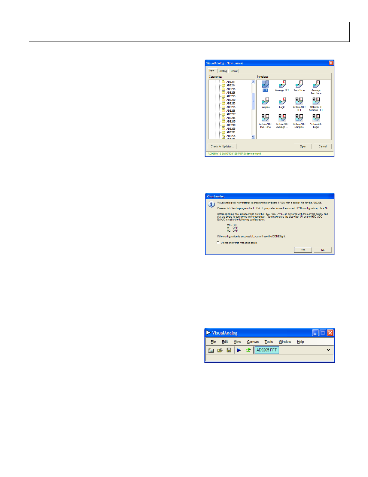
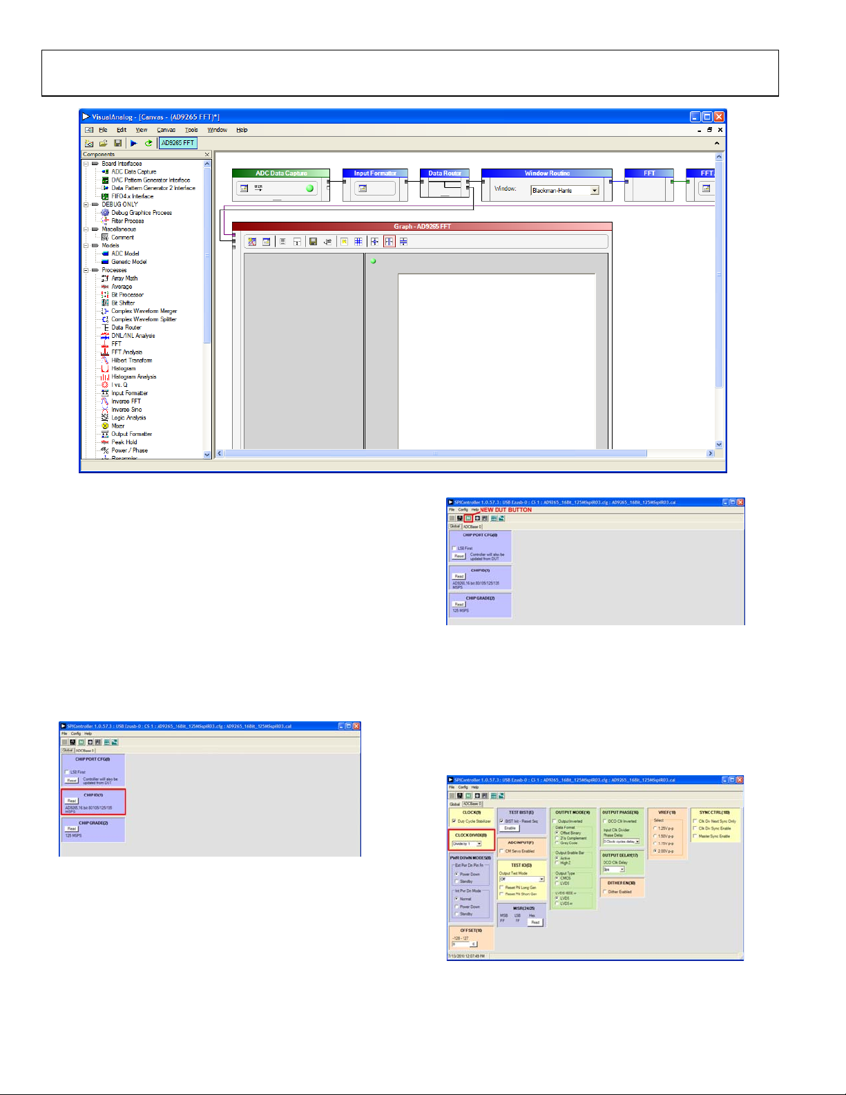
1. Open VisualAnalog on the connected PC. The appropriate
part type should be listed in the status bar of the
VisualAnalog – New Canvas window. Select the template
that corresponds to the type of testing to be performed
(see Figure 4 where the AD9265 is shown as an example).
Figure 4. VisualAnalog – New Canvas Window
2. After the template is selected, a message appears asking if
the default configuration can be used to program the FPGA
(see Figure 5). Click Yes and the window closes.
Figure 5. VisualAnalog Default Configuration Message
3. To change features to settings other than the default settings,
click the Expand Display button, located on the bottom
right corner of the window, to see what is shown in Figure 7.
Detailed instructions for changing the features and capture
settings can be found in the AN-905 Application Note,
VisualAnalog Converter Evaluation Tool Version 1.0 User
Manual. After the changes are made to the capture settings,
click Collapse Display (see Figure 7).
08699-004
08699-005
08699-006
Figure 6. VisualAnalog Window Toolbar, Collapsed Display
Rev. 0 | Page 7 of 28
UG-074 Evaluation Board User Guide
08699-007
Figure 7. VisualAnalog, Main Window
Setting Up the SPI Controller Software
After the ADC data capture board setup is complete, set up the
SPIController software using the following procedure:
1. Open the SPIController software by going to the Start menu
or by double-clicking the SPIController software desktop
icon. If prompted for a configuration file, select the appropriate
one. If not, check the title bar of the window to determine
which configuration is loaded. If necessary, choose Cfg
Open from the File menu and select the appropriate file
based on your part type. Note that the CHIP ID(1) field
should be filled to indicate whether the correct
SPIController configuration file is loaded (see Figure 8).
Figure 8. SPIController, CHIP ID(1) Box
2. Click the New DUT button in the SPIController window
(see Figure 9).
08699-009
Figure 9. SPIController, New DUT Button
3. In the ADCBase 0 tab of the SPIController window, find the
CLOCK DIVIDE(B) box (see Figure 10). If using the clock
divider, use the drop-down box to select the correct clock
divide ratio, if necessary. See the appropriate part data sheet;
the AN-878 Application Note, High Speed ADC SPI Control
Software; and the AN-877 Application Note, Interfacing to
High Speed ADCs via SPI, for additional information.
08699-008
Rev. 0 | Page 8 of 28
Figure 10. SPIController, CLOCK DIVIDE(B) Box
08699-010
Evaluation Board User Guide UG-074
4. Note that other settings can be changed on the ADCBase 0
tab (see Figure 10). See the appropriate part data sheet; the
AN-878 Application Note, High Speed ADC SPI Control
Software; and the AN-877 Application Note, Interfacing to
High Speed ADCs via SPI, for additional information on the
available settings.
08699-011
Figure 11. SPIController, Example ADCBase 0 Page
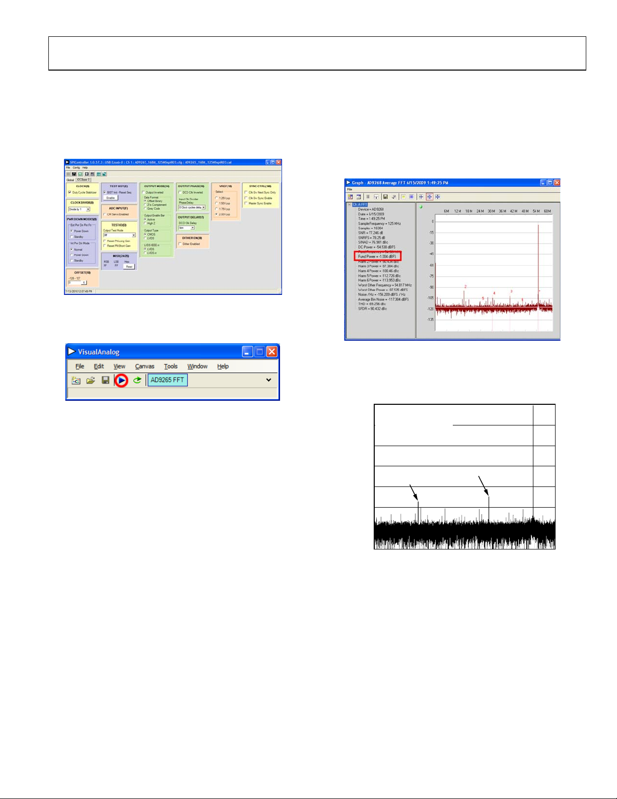
5. Click the Run button in the VisualAnalog toolbar
(see Figure 12).
08699-012
Figure 12. Run Button (Encircled in Red) in VisualAnalog Toolbar, Collapsed
Display
Adjusting the Amplitude of the Input Signal
The next step is to adjust the amplitude of the input signal
as follows:
1. Adjust the amplitude of the input signal so that the
fundamental is at the desired level. (Examine the Fund Power
reading in the left panel of the Graph - AD9265 Average FFT
window, see Figure 13.)
Figure 13. Graph Window of VisualAnalog
2. Click the disk icon within the Graph window to save the
performance plot data as a .csv formatted file. See Figure 14
for an example.
0
125MSPS
70.1MHz @ –1dBFS
–20
SNR = 76.5dB (77.5dBFS)
SFDR = 88.0dBc
–40
08699-013
–60
SECOND HARMONIC
–80
AMPLITUDE (dBFS)
–100
–120
–140
0 102030405060
Figure 14. Typical FFT, AD9265/AD9255
THIRD HARMONIC
FREQUENCY (MHz)
08699-014
Rev. 0 | Page 9 of 28

UG-074 Evaluation Board User Guide
Troubleshooting Tips
If the FFT plot appears abnormal, do the following:
• If you see a normal noise floor when you disconnect the
signal generator from the analog input, be sure you are not
overdriving the ADC. Reduce the input level, if necessary.
• In VisualAnalog (see Figure 7), click the Settings button
in the Input Formatter block. Check that Number Format
is set to the correct encoding (offset binary by default).
Repeat for the other channel.
If the FFT appears normal but the performance is poor, check
the following:
• Make sure an appropriate filter is used on the analog input.
• Make sure the signal generators for the clock and the
analog input are clean (low phase noise).
• Change the analog input frequency slightly if noncoherent
sampling is being used.
• Make sure the SPI config file matches the product being
evaluated.
If the FFT window remains blank after clicking Run, do the
following:
• Make sure the evaluation board is securely connected to
the HSC-ADC-EVALCZ board.
• Make sure the FPGA has been programmed by verifying
that the DONE LED is illuminated on the HSC-ADC-
EVALCZ board. If this LED is not illuminated, make sure
the U4 switch on the board is in the correct position for
USB CONFIG.
• Make sure the correct FPGA program was installed by
selecting the Settings button in the ADC Data Capture
block in VisualAnalog (see Figure 7). Then select the
FPGA tab and verify that the proper FPGA bin file is
selected for the part.
If VisualAnalog indicates that the FIFO Capture timed out
(via a pop-up window), do the following:
1. Make sure all power and USB connections are secure.
2. Probe the DCO signal at P25 (Pin 2) on the evaluation
board and confirm that a clock signal is present at the
ADC sampling rate.
Rev. 0 | Page 10 of 28

Evaluation Board User Guide UG-074
EVALUATION BOARD SCHEMATICS AND ARTWORK
08699-015
Figure 15. Board Power Input and Supply Circuits
Rev. 0 | Page 11 of 28

UG-074 Evaluation Board User Guide
08699-016
Figure 16. DUT and Related Circuits
Rev. 0 | Page 12 of 28

Evaluation Board User Guide UG-074
08699-017
SPI CIRCUITRY
Figure 17. SPI Interface Circuit
Rev. 0 | Page 13 of 28

UG-074 Evaluation Board User Guide
08699-018
Figure 18. Analog Input Circuits
Rev. 0 | Page 14 of 28

Evaluation Board User Guide UG-074
CLK+
C22
0.1UF
CLKOUT+
R85A
DNI
0
0
R85
CLK-
DNI
100
R73
C23
0.1UF
CLKOUT-
R86A
0
DNI
0
R86
08699-019
2
3
CR1
1
HSMS-2812BLK
DNI
R93
24.9
GND
0
CLKIN+
R30
R28
0
DNI
DNI
DNI
100
R72
T5
DNI
SEC
R17
DNI
24.9
GND
0
R31
R29
TP5
1
0.1UF
GND
C6
PRI
CLKIN-
0
DNI
TP6
BLK
GND
1
WHT
MABA-007159-000000
0.1UF
T9
1
SEC
BALUN CLOC K CIRCUITR Y
XTAL_IN
C70
DNI
0.1UF
125MHZ
Y1
3
3V_CLK
C16
OUT
GND
VCC
4
GND
2
TRISTATE CTRL
0.1UF
1
GND
1.00K
R7
1
2
5
43
PRI
MABA-007159-000000
C18
0.1UF
XTAL_IN
GND
R25
49.9
5432
1
J6
P6
642
T1
DNI
3
0
R48
GND
C30
GND
1
J7
DNI
C27
ADT1-1WT+
GND
1
DNI
0.1UF
GND
R12
49.9
DNI
5
43
2
CLOC K INPU T
SW-102-08-G-S
Figure 19. Default Clock Path Input Circuits
Rev. 0 | Page 15 of 28

UG-074 Evaluation Board User Guide
GND
1
J603
DNI
5432
57.6
DNI
AC
CR60 1
SML-LXT0805IW-TR
GND
CLKOUT+
CLKOUT-
C66 0
T601
200
C604
0.1U F
4
6
U60 3
3V_CLK
5
VCC
C619
0.1U F
GND
NC7WZ16P6X
Y2
Y1
A1
1
0
R629 R630
TP60 1
1
WHT
GND
2
GND
A2
3
GND
4.12K
R610
TP60 3
1
WHT
TP60 2
1
WHT
1
44
U601
3
VCP
RSET
45
43
37
36
31
30
VS
25
3V_CLK
24
10
40
21
VS_LVPECL
REF_SE L
6
1.00 K
R604
3V_CL K
C603
0.1U F
R61 4
GND
5.11K
R611
CP
46
2
LD
CPRSE T
REFMO N
REFIN_N_REF2
REFIN_REF 1
48
47
C602
394142
4
5
CP
OUT1
OUT0
OUT0_ N
STATU S
CLK
LF
BYPAS S
8
9
12
11
LF
9517_CLK
BYPASS_LDO
3V_CLK
0.1U F
R61 6
200
OUT1_ N
CLK_ N
C621
R60 7R606R60 5
200
GND
PECL_OUT1
PECL_OUT1_N
OUT3
OUT2
OUT3_ N
OUT2_ N
0.1U F
GND
1.00 K
1.00 K
1.00 K
OUT6_OUT6A
OUT5_OUT5A
OUT4_OUT4A
OUT5_N_OUT5B
OUT4_N_OUT4B
RESET_ N
SYNC_ N
PD_N
7
17
18
3V_CLK
AD9517_PWDNBUF
C623
PECL_OUT1
WHT
1
TP60 4
100
R64 0
FIFO_SDO
15
28292627333235342322201938
AD9517-4BCPZ
SDO
OUT7_OUT7A
OUT7_N_OUT7B
OUT6_N_OUT6B
PAD
PAD
SDIO
SCLK
CS_N
16
13
14
FIFO_SD I
FIFO_SCLK
1.00 K
R609
0
R60 8
AD9517_CSB
GND
R651
DNI
0.1U F
DNI
43
0.1U F
GND
GND
1
SEC
PRI
5
MABA-007159-000000
DNI
DNI
TP60 5
C620
J602
1
9517_CLK
DNI
1
200
R638
WHT
C624
0.1U F
DNI
GND
DNI
0.1U F
R633
5432
200
R639
PECL_OUT1_N
DNI
57.6
GND
GND
DNI
GND
C614
C615
0.1U F
3V_CLK
C60 8
0
R627
C61 0
C60 9
0.1U F
0.1U F
LF
C617
C616
0.1U F
0.1U F
C611
0.1U F
0.1U F
C61 2
1500PF
C607
100
R626
R625
200
1800PF
.033UF
C606
C605
0
R623
08699-020
GNDGND
C618
0.1U F
0.1U F
C61 3
0.1U F
0.1U F
.22U F
C622
GND
C601
0.1UF
CP
BYPASS_LDO
PECL/CML/LVD S CL K CIRCUITR Y
LKIN+
LKIN-
CHARGE PUMP FILTER
Figure 20. Optional AD9517 Clock Input Circuit
Rev. 0 | Page 16 of 28

Evaluation Board User Guide UG-074
GND
08699-021
0.1UF0.1UF0.1UF0.1UF
D0_O
D2_O
D1_O
DCO_O
5
3
C10 C29 C31C11
2
U2
O2O1O0
7
22
35
VCC
50
V_DIG
I1
495152
54
55
D8_O
D9_O
D7_O
D6_O
D5_O
D4_O
D3_O
10
986
D10_O
141312
15
O9O8O7O6O5O4O3
O11
O10
I11
I10
I9I8I7I6I5I0I4I3I2
4344454748
404142
OR_O
D15_O
D14_O
D13_O
D12_O
D11_O
191716
O12
I12
272624
232120
O19
O18
O17
O16
O15
O14
O13
I19
I18
I17
I16
I15
I14
I13
30313334363738
74VCX162827MTDX
53
46
39
GND
32
25
GND
18
11
4
OE1_N
OE4_N
OE3_N
OE2_N
1
282956
GND
CR2
AC
GND
SML-LXT0805IW-TR
GND
GND
10K
10K
R27
R26
BLK
TP7
C32
OUTPUT BUFFERS
22
R71
8
63
22
R49
22
RN4
RN4
1
72
54
22
RN4
22
RN4
8
63
22
22
RN10
1
RN10
72
54
22
22
RN10
RN10
8
63
22
222222
RN5
RN5
1
54
72
22
RN5
RN5
8
63
22
22
RN9
RN9
1
72
54
22
RN9
22
RN9
OTR LED CIRCUIT
GND
249
R55
4
6
U7
3V_AVDD
5
VCC
0.1UF
GND
NC7WZ16P6X
Y2
Y1
A1
1
0
R53
GND
2
GND
A2
3
GND
10K
R40
OR_O
1
D9
DCO
1
2
DNI
D3
D2
D1
D0
D8
D11
D6D4D7
D5
D10
D15
OR
D14
D12
D13
P25
2
DNI
P15
Figure 21. Output Buffer Circuits
Rev. 0 | Page 17 of 28

UG-074 Evaluation Board User Guide
P1
DG1
DG2
P1
BG2
BG1
P1
D2
D1
PLUG HEADER
DG3
DG1 0
GNDGND
6469169-16469169-1 6469169-1
DG9
DG8
DG7
DG6
DG5
DG4
PLUG HEADER
BG3
BG1 0
BG9
BG8
BG7
BG6
BG5
BG4
PLUG HEADER
D9D8D7D6D5D4D3
D10
P2
DG6
DG5
DG4
DG3
DG2
DG1
P2
BG1
BG6
BG5
BG4
BG3
BG2
P2
D2
D1
08699-022
PLUG HEADER
6469169-1
DG9
DG8
DG7
DG1 0
GND
PLUG HEADER
6469169-1
BG9
BG8
BG7
BG1 0
GND
PLUG HEADER
6469169-1
D9D8D7D6D5D4D3
D10
P1
B2
B1
P1
C2
C1
P1
A1
PLUG HEADER
6469169-1
B9B8B7B6B5B4B3
B10
FIFO_SDO
FIFO_FPGA_SCLK
FIFO_FPGA_SDI
FIFO_SCLK
FIFO_SD I
PLUG HEADER
6469169-1
C9C8C7C6C5C4C3
C10
P2
B2
B1
P2
C2
C1
D2_O
D0_O
PLUG HEADER
6469169-1
A2
A9A8A7A6A5A4A3
A10
AD9517_CSB
FIFO_CSB
FIFO_FPGA_SDO
FIFO_FPGA_CSB
P2
A2
A1
D1_O
PLUG HEADER
6469169-16469169-1
B9B8B7B6B5B4B3
B10
PLUG HEADER
6469169-1
C9C8C7C6C5C4C3
C10
D4_O
D6_O
OR_O
D14_ O
D12_ O
D10_ O
D8_O
PLUG HEADER
A9A8A7A6A5A4A3
A10
D3_O
D5_O
DCO_ O
D7_O
D9_O
D11_ O
D13_ O
D15_ O
Figure 22. Capture Board Connector
Rev. 0 | Page 18 of 28

Evaluation Board User Guide UG-074
Figure 23. Top Side
08699-023
Rev. 0 | Page 19 of 28

UG-074 Evaluation Board User Guide
Figure 24. Ground Plane (Layer 2)
08699-024
Rev. 0 | Page 20 of 28

Evaluation Board User Guide UG-074
Figure 25. Power Plane (Layer 3)
08699-025
Rev. 0 | Page 21 of 28

UG-074 Evaluation Board User Guide
Figure 26. Power Plane (Layer 4)
8699-026
Figure 27. Ground Plane (Layer 5)
Rev. 0 | Page 22 of 28
08699-027

Evaluation Board User Guide UG-074
08699-028
Figure 28. Bottom Side
Rev. 0 | Page 23 of 28

UG-074 Evaluation Board User Guide
ORDERING INFORMATION
BILL OF MATERIALS
Table 1. AD9265/AD9255 BOM
Item No. Qty Reference Designator Description Manufacturer/Part No.
1 1 Not applicable Printed circuit board
2 3 C2, C4, C15
3 46
4 3 C39, C41, C74
5 8
6 1 C605
7 1 C606
8 1 C607
9 1 C622
10 9
11 2 C72, C73 Capacitor, 0603, X5R, 10 μF Panasonic/ECJ-1VB0J106M
12 3 C75, C82, C83
13 1 CR1
14 2 CR2, CR601 LED, red, surface mount Lumex/SML-LXT0805IW-TR
15 4 CR3, CR4, CR5, CR6
16 1 CR7
17 1 DUT Analog-to-digital converter
18 9
19 1 F1
20 1 FL1
21 4 J1, J3, J6, J9
22 2 JP5, JP8 3-pin solder jumper, JPRSLD03 Not applicable
23 2 P1, P2
C3, C5, C8, C10, C11, C12,
C14, C16, C18, C22, C23,
C27, C29, C31, C32, C33,
C34, C38, C40, C42, C43,
C45, C46, C47, C48, C60,
C61, C66, C71, C78, C96,
C601, C602, C608, C609,
C610, C611, C612, C613,
C614, C615, C616, C617,
C618, C619, C621
C53, C54, C62, C64, C65,
C67, C68, C69
C7, C9, C55, C56, C57,
C58, C59, C63, C84
E1, E4, E5, E6, E7, E8, E9,
E10, E12
Ceramic capacitor, multilayer,
NP0, 0402, 10 pF
Ceramic capacitor, 0402, 0.1 μF Panasonic/ECJ-0EX1C104K
Ceramic capacitor, mono,
0402, 1 μF
Capacitor, 0603, X5R, 4.7 μF Panasonic/ECJ-1VB0J475M
Ceramic capacitor, multilayer,
X7R, 0402, 1800 pF
Ceramic capacitor, 0.033 μF,
C0402
Ceramic capacitor, 0402,
1500 pF
Ceramic capacitor, 0.22 μF,
C0402
Ceramic capacitor,
monolithic, 10 μF, C0805
Ceramic capacitor, multilayer,
X7R, 0402, 0.01 μF
Diode Schottky, dual series,
SOT23
Diode, recovery rectifier,
DO214AA3
LED, green, surface mount,
LED0603
Inductor ferrite bead,
100 MHz, L0805
Fuse polyswitch, PTC device
1812, 1.1 A,
FTYCOMINISMDC110F
Filter noise suppression, LC
combined type
Conn-PCB, SMA ST, edge
mount, CNSAMTECSMA-JPXST-EM1-MKT
Conn PCB,60-pin RA connector,
CNTYCO1469169-1
Phycomp (Yageo)/CC0402JRNP09BN100
Murata/GRM155R60J105KE19D
Panasonic/ECJ-0EB1E182K
Panasonic/0402YD333KAT2A
Panasonic/ECJ-0EB1H152K
Panasonic/ECJ-0EB0J224K
Murata/GRM21BR61C106KE15L
Panasonic/ECJ-0EB1E103K
Avago/HSMS-2812BLK
Micro Commercial Components Corp/S2A-TP
Panasonic/LNJ308G8TRA
Analog Devices/AD9265BCPZ-80, AD9265BCPZ-105,
AD9265BCPZ-125, AD9255BCPZ-80, AD9255BCPZ-105, or
AD9255BCPZ-125 per build instructions
Panasonic/EXC-ML20A390U
Tyco Electronics/MINISMDC110F-2
Murata/BNX016-01
Samtec/SMA-J-P-X-ST-EM1
Tyco/6469169-1
Rev. 0 | Page 24 of 28

Evaluation Board User Guide UG-074
Item No. Qty Reference Designator Description Manufacturer/Part No.
24 1 P26
25 13
26 1 P4
27 3 P5, P10, P30
28 2 P8, P9
29 22
30 4 R13, R14, R15, R16 Resistor film, SMD, 0402, 33 Ω Panasonic/ERJ-2GEJ330X
31 15
32 4 R3, R8, R22, R23
33 2 R25, R33
34 2 R49, R71
35 2 R55, R67
36 1 R610
37 1 R611
38 4 R614, R616, R625, R630
39 2 R626, R640 Resistor, film, SMD 0402, 100 Ω Venkel/CR0402-16W-1000FPT
40 3 R64, R65, R66
41 9
42 1 R74
43 1 R75
44 4 RN4, RN5, RN9, RN10
45 3 T2, T3, T9 XFMR RF 1:1, ETC1 M/A-COM/MABA-007159-000000
46 1 U1
47 1 U2
48 1 U3
49 1 U4
50 3 U5, U7, U603
P3, P6, P7, P11, P12, P14, P18,
P19, P27, P28, P29, P31, P32
R1, R6, R10, R11, R30, R31,
R46, R47, R48, R52, R53, R77,
R79, R81, R83, R85, R86,
R608, R623, R627, R629, JP4
R26, R27, R35, R36, R37, R38,
R39, R40, R43, R57, R58, R59,
R68, R69, R70
R7, R61, R62, R63, R604,
R605, R606, R607, R609
Conn-PCB power jack surface
mount, CN-2MM-PWR-JACK
Conn-PCB header, 2-position,
CNSAMTEC1X2H330LD36
Conn-PCB header,
ST male, 9-position,
CNSAMTEC3X3H338LD36
Conn-PCB Berg header,
ST male, 3-position,
CNBERG1X3H205LD36
Conn-PCB header, 6-position,
CNWIELAND5313625
Resistor film, SMD, 0402, 0 Ω Panasonic/ERJ-2GE0R00X
Resistor, precision, thick film
chip, R0402, 10 kΩ
Resistor, precision, thick film
chip, R0402, 10 Ω
Resistor, precision, thick film
chip, R0603, 49.9 Ω
Resistor, precision, thick film
chip, R0402, 22 Ω
Resistor, precision, thick film
chip, R0603, 249 Ω
Resistor, precision, thick film
chip, R0402, 4.12 kΩ
Resistor, precision, thick film
chip, R0402, 5.11 kΩ
Resistor, precision, thick film
chip, R0402, 200 Ω
Resistor, precision, thick film
chip, R0402, 100 kΩ
Resistor, precision, thick film
chip, R0402, 1.00 kΩ
Resistor, precision, thick film
chip, R0402, 147 kΩ
Resistor, precision, thick film
chip, R0402, 28 kΩ
Resistor network, 8-pin/4
resistor surface mount,
RESNET742-4, 22 Ω
IC, 2.6 GHz, ultralow distortion,
differential IF/RF amplifier,
QFN16_3X3_PAD1_5X1_5
IC-TTL low volt 20-bit buffer,
TSSOP56
IC TinyLogic UHS dual buffer,
SC70
IC, low dropout CMOS, lin reg,
SO8NB-PAD3_1X2_41
IC TinyLogic UHS dual buffer,
SC70
CUI/PJ-002AH-SMT
Samtec/TSW-102-08-G-S
Samtec/TSW-103-08-G-T
Samtec/TSW-103-08-G-S
Wieland/Z5.531.3625.0
Panasonic/ERJ-2RKF1002X
Panasonic/ERJ-2RKF10R0X
Panasonic/ERJ-3EKF49R9V
Panasonic/ERJ-2RKF22R0X
Panasonic/ERJ-3EKF2490V
Panasonic/ERJ-2RKF4121X
Panasonic/ERJ-2RKF5111X
Panasonic/ERJ-2RKF2000X
Panasonic/ERJ-2RKF1003X
Panasonic/ERJ-2RKF1001X
Panasonic/ERJ-2RKF1473X
Panasonic/ERJ-2RKF2802X
CTS/742C083220JCT
Analog Devices/ADL5562_PRELIM
Fairchild/74VCX162827MTDX
Fairchild/NC7WZ07P6X
Analog Devices/ADP1706ARDZ-3.3-R7
Fairchild/NC7WZ16P6X
Rev. 0 | Page 25 of 28

UG-074 Evaluation Board User Guide
Item No. Qty Reference Designator Description Manufacturer/Part No.
51 1 U6
52 1 U601
53 1 U8
54 2 U9, U10
551 C1
561 C13
571 C49, C50 Ceramic capacitor, 1000 pF Panasonic/ECU-E1E102KBQ
581
591 C77, C79, C80, C81 Capacitor, 0603, X5R, 10 μF Panasonic/ECJ-1VB0J106M
601 E2, E3, E11
611 J2, J7, J602, J603
621 L1, L5, L6 Chip inductor, 15 nH, L7144 Coilcraft/0603CS-15NXGLU
631 L2, L3
641 L8, L9 Chip inductor, 36 nH, L7144 Coilcraft/0603CS-36NXGLU
651 P15, P16, P17, P25
661 R4, R12, R94, R95
671 R17, R18, R19, R93
681 R20, R21
691
701 R44, R45, R638, R639
711 R5, R72, R73 Resistor, film, SMD, 0402, 100 Ω Venkel/CR0402-16W-1000FT
721 R50, R51 Do not install (TBD_R0402)
731 R54, R56 Resistor, film, SMD, 0603, 0 Ω Multicomp/MC0603WG00000T5E-TC
741 R633, R651
751 R76
C6, C25, C30, C51, C52, C70,
C97, C603, C604, C620,
C623, C624, C660
R28, R29, R32, R34, R41, R42,
R78, R80, R82, R84, R85A,
R86A, R96, JP1, JP25
IC compact, 600 mA, 3 MHz,
step-down dc-to-dc
converter, 5-lead TSOT
IC, 12-output clock gen
with int 1.6 GHz VCO,
QFN48_7X7_PAD5_1X5_1
IC, low dropout CMOS, lin reg,
SO8NB-PAD3_1X2_41
IC, low dropout CMOS, lin reg,
SO8NB-PAD3_1X2_41
Capacitor, chip, mono,
ceramic, C0G, 0402, 2.2 pF
Capacitor, chip, mono,
ceramic, C0G, 0402, 100 pF
Ceramic capacitor, 0402, 0.1 μF Panasonic/ECJ-0EX1C104K
Inductor ferrite bead,
100 MHz, L0805
Conn-PCB, SMA ST edge
mount, CNSAMTECSMA-JPXST-EM1-MKT
Inductor, SMT power, 2.2 μH,
LSMSQ79H57
Conn-PCB header, 2-position,
CNSAMTEC1X2H330LD36
Resistor, precision, thick film
chip, R0603, 49.9 Ω
Resistor, precision, thick film
chip, R0402, 24.9 Ω
Resistor, precision, thick film
chip, R0402, 1.00 kΩ
Resistor, film, SMD, 0402, 0 Ω Panasonic/ERJ-2GE0R00X
Resistor, precision, thick film
chip, R0402, 200 Ω
Resistor, precision, thick film
chip, R0402, 57.6 Ω
Resistor, precision, thick film
chip, R0402, 100 kΩ
Analog Devices/ADP2108AUJZ-1.8-R7
Analog Devices/AD9517-4BCPZ
Analog Devices/ADP1708ARDZ-R7
Analog Devices/ADP1706ARDZ-1.8-R7
Murata/GJM1555C1H2R2WB01
Murata/GRM1555C1H101JD01D
Panasonic/EXC-ML20A390U
Samtec/SMA-J-P-X-ST-EM1
Coilcraft/EPL2014-222MLB
Samtec/TSW-102-08-G-S
Panasonic/ERJ-3EKF49R9V
Panasonic/ERJ-2RKF24R9X
Panasonic/ERJ-2RKF1001X
Panasonic/ERJ-2RKF2000X
Panasonic/ERJ-2RKF57R6X
Panasonic/ERJ-2RKF1003X
Rev. 0 | Page 26 of 28

Evaluation Board User Guide UG-074
Item No. Qty Reference Designator Description Manufacturer/Part No.
761 T1 XFMR RF, MINICD542 Mini-Circuits/ADT1-1WT+
771 T4, T5, T601 XFMR RF 1:1, ETC1 M/A-COM/MABA-007159-000000
781 T6 XFMR RF, MINICD542 Mini-Circuits/ADT1-1WT+
791
TP1, TP2, TP3, TP6, TP7,
TP10, TP11
801
TP4, TP5, TP9, TP19, TP601,
TP602, TP603, TP604, TP605
811 Y1
1
Do not insert.
Conn-PCB, test point black,
CNLOOPTP
Conn-PCB, test point white,
CNLOOPTP
IC clock OSC ACMOS/LSTTL
compatible, 125 MHz,
XTALCB3LV_H90
Components Corp/TP-104-01-00
Components Corp/TP-104-01-09
Valpey Fisher/VFAC3HL-125MHZ
Rev. 0 | Page 27 of 28

UG-074 Evaluation Board User Guide
NOTES
ESD Caution
ESD (electrostatic discharge) sensitive device. Charged devices and circuit boards can discharge without detection. Although this product features patented or proprietary protection
circuitry, damage may occur on devices subjected to high energy ESD. Therefore, proper ESD precautions should be taken to avoid performance degradation or loss of functionality.
Legal Terms and Conditions
By using the evaluation board discussed herein (together with any tools, components documentation or support materials, the “Evaluation Board”), you are agreeing to be bound by the terms and conditions
set forth below (“Agreement”) unless you have purchased the Evaluation Board, in which case the Analog Devices Standard Terms and Conditions of Sale shall govern. Do not use the Evaluation Board until you
have read and agreed to the Agreement. Your use of the Evaluation Board shall signify your acceptance of the Agreement. This Agreement is made by and between you (“Customer”) and Analog Devices, Inc.
(“ADI”), with its principal place of business at One Technology Way, Norwood, MA 02062, USA. Subject to the terms and conditions of the Agreement, ADI hereby grants to Customer a free, limited, personal,
temporary, non-exclusive, non-sublicensable, non-transferable license to use the Evaluation Board FOR EVALUATION PURPOSES ONLY. Customer understands and agrees that the Evaluation Board is provided
for the sole and exclusive purpose referenced above, and agrees not to use the Evaluation Board for any other purpose. Furthermore, the license granted is expressly made subject to the following additional
limitations: Customer shall not (i) rent, lease, display, sell, transfer, assign, sublicense, or distribute the Evaluation Board; and (ii) permit any Third Party to access the Evaluation Board. As used herein, the term
“Third Party” includes any entity other than ADI, Customer, their employees, affiliates and in-house consultants. The Evaluation Board is NOT sold to Customer; all rights not expressly granted herein, including
ownership of the Evaluation Board, are reserved by ADI. CONFIDENTIALITY. This Agreement and the Evaluation Board shall all be considered the confidential and proprietary information of ADI. Customer may
not disclose or transfer any portion of the Evaluation Board to any other party for any reason. Upon discontinuation of use of the Evaluation Board or termination of this Agreement, Customer agrees to
promptly return the Evaluation Board to ADI. ADDITIONAL RESTRICTIONS. Customer may not disassemble, decompile or reverse engineer chips on the Evaluation Board. Customer shall inform ADI of any
occurred damages or any modifications or alterations it makes to the Evaluation Board, including but not limited to soldering or any other activity that affects the material content of the Evaluation Board.
Modifications to the Evaluation Board must comply with applicable law, including but not limited to the RoHS Directive. TERMINATION. ADI may terminate this Agreement at any time upon giving written notice
to Customer. Customer agrees to return to ADI the Evaluation Board at that time. LIMITATION OF LIABILITY. THE EVALUATION BOARD PROVIDED HEREUNDER IS PROVIDED “AS IS” AND ADI MAKES NO
WARRANTIES OR REPRESENTATIONS OF ANY KIND WITH RESPECT TO IT. ADI SPECIFICALLY DISCLAIMS ANY REPRESENTATIONS, ENDORSEMENTS, GUARANTEES, OR WARRANTIES, EXPRESS OR IMPLIED, RELATED
TO THE EVALUATION BOARD INCLUDING, BUT NOT LIMITED TO, THE IMPLIED WARRANTY OF MERCHANTABILITY, TITLE, FITNESS FOR A PARTICULAR PURPOSE OR NONINFRINGEMENT OF INTELLECTUAL
PROPERTY RIGHTS. IN NO EVENT WILL ADI AND ITS LICENSORS BE LIABLE FOR ANY INCIDENTAL, SPECIAL, INDIRECT, OR CONSEQUENTIAL DAMAGES RESULTING FROM CUSTOMER’S POSSESSION OR USE OF
THE EVALUATION BOARD, INCLUDING BUT NOT LIMITED TO LOST PROFITS, DELAY COSTS, LABOR COSTS OR LOSS OF GOODWILL. ADI’S TOTAL LIABILITY FROM ANY AND ALL CAUSES SHALL BE LIMITED TO THE
AMOUNT OF ONE HUNDRED US DOLLARS ($100.00). EXPORT. Customer agrees that it will not directly or indirectly export the Evaluation Board to another country, and that it will comply with all applicable
United States federal laws and regulations relating to exports. GOVERNING LAW. This Agreement shall be governed by and construed in accordance with the substantive laws of the Commonwealth of
Massachusetts (excluding conflict of law rules). Any legal action regarding this Agreement will be heard in the state or federal courts having jurisdiction in Suffolk County, Massachusetts, and Customer hereby
submits to the pers onal jurisdiction and venu e of such courts. The United Nations Conventi on on Contracts for the Internation al Sale of Goods shall not apply to this Agreement and is expressly disclaimed.
©2011 Analog Devices, Inc. All rights reserved. Trademarks and
registered trademarks are the property of their respective owners.
UG08699-0-1/11(0)
Rev. 0 | Page 28 of 28
 Loading...