

Evaluation Board User Guide
UG-018
One Technology Way • P. O . Box 9106 • Norwood, MA 02062-9106, U.S.A. • Tel : 781.329.4700 • Fax : 781.461.3113 • www.analog.com
Evaluation Board for Dual High Speed Differential Amplifiers
FEATURES
Enables quick breadboarding/prototyping
User-defined circuit configuration
Edge-mounted SMA connector provisions
Easy connection to test equipment and other circuits
Two independent circuits enhance flexibility
GENERAL DESCRIPTION
The EB-D24CP44-2Z is designed, to aid in the evaluation of
dual high speed differential amplifiers. The EB-D24CP44-2Z
is a bare board (that is, there are no components soldered to
the board) that enables users to quickly prototype a variety of
differential amplifier circuits, which minimizes risk and
reduces time to market. The EB-D24CP44-2Z evaluation
board supports any of Analog Devices, Inc., dual high speed
differential amplifiers in 4 mm × 4 mm lead frame chip scale
packages (LFCSP).
Figure 1 shows the component side and circuit side of the
evaluation board. Figure 2 shows the evaluation board
schematic.
The 4-layer evaluation board accepts edge-mounted SMA connectors on both inputs and outputs, which allows efficient and
quick connection to test equipment or other circuitry.
The board ground plane, component placement, and power
supply bypassing have been optimized for maximum circuit
flexibility and performance. The evaluation board uses a variety
of SMT component case sizes: 0402, 0508, 0805, and 7343.
Figure 3 and Figure 5 show the evaluation board assembly
drawings. The metal layout pattern for connecting the board to
the op amp and to the supporting circuitry is shown in Figure 4
and Figure 6.
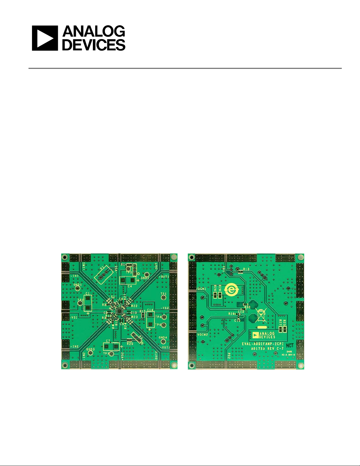
DIGITAL PICTURE OF THE EVALUATION BOARD
COMPONENT SIDE
NOTES
1. THE EVALUATION BOARD SIL KSCREEN PART NUMBER LABELING ON YOUR BO ARD MAY BE DIFF ERENT FROM WHAT IS SHOWN HERE.
Figure 1. Component and Circuit Side of PCB
CIRCUIT SIDE
08142-006
See the last page for an important warning and disclaimers. Rev. A | Page 1 of 1

UG-018 Evaluation Board User Guide
TABLE OF CONTENTS
Features .............................................................................................. 1
General Description ......................................................................... 1
Digital Picture of the Evaluation Board ......................................... 1
Revision History ............................................................................... 2
REVISION HISTORY
2/10—Rev. 0 to Rev. A
Changes to General Description and Figure 1 ............................. 1
7/09—Revision 0: Initial Version
Evaluation Board Schematic ............................................................3
Assembly Drawing and Board Layout ............................................4
ESD Caution...................................................................................4
Rev. A | Page 2 of 2

Evaluation Board User Guide UG-018
EVALUATION BOARD SCHEMATIC
2
2
S
S
V
V
–
+
*
D
1
N
S
G
V
A
+
1
2
1
1
P
P
I
0
3
N
R
D
)
5
P
(T
1
S
V
–
A
M
S
1
IS
/D
1
D
P
+
F
4
µ
C
0
1
1
S
V
+
*
*
4
3
1
1
R
R
1
D
P
1
2
2
2
P
P
*
5
0
1
S
V
–
3
1
P
1
T
U
O
–
A
M
S
1
T
U
O
–
*
6
1
R
D
N
G
A
6
C
D
N
G
A
1
S
V
–
3
2
P
1
R
R2
2
D
P
2
3
1
3
3
3
P
P
P
I
D
1
N
N
D
R2
G
A
F
µ
D
.1
N
0
G
A
*
1
0
1
0
2
R
*
5
R
*
1
R
1
IN
+
D
N
G
A
A
M
S
1
IN
+
Figure 2. Dual Differential Amplifier Universal Evaluation Board Schematic
1
-0
0
2
4
1
8
0
)
4
P
(T
2
S
V
–
1
T
U
O
+
A
M
S
I
D
2
N
2
N
D
R
1
T
O
+
*
7
1
R
1
9
1
1
0
2
1
1
2
1
2
2
1
3
2
1
4
2
G
A
1
1
P
M
T
C
VO
A
M
S
1
M
C
O
V
T
U
O
/D
IS
S
V
–
S
V
–
B
F
–
IN
+
*
6
R
1
IN
–
A
M
S
1
IN
–
D
N
G
A
F
µ
2
1
.1
C
0
7
8
1
1
1
1
T
M
U
C
O
O
–
+
V
1
D
P
1
1
B
IN
F
–
+
1
2
*
9
R
*
2
R
D
N
G
A
)
2
P
(T
1
S
+V
+
4
F
1
µ
C
0
1
3
F
1
µ
C
.1
0
D
N
G
A
I
9
2
N
R
D
5
6
1
1
2
2
S
S
V
V
–
–
1
Z
1
1
S
S
V
V
+
+
3
4
*
7
R
A
M
S
F
µ
.1
2
0
C
F
µ
0
1
1
C
+
D
N
G
A
D
N
G
A
2
IS
2
T
/D
U
2
D
O
–
P
A
A
M
M
S
S
I
3
N
2
2
D
R
T
U
O
–
*
8
1
R
4
3
1
1
2
2
T
D
U
P
O
–
2
T
U
O
M
2
C
O
2
S
V
2
S
V
2
B
F
IN
2
B
F
–
5
2
IN
+
2
IN
+
2
2
IN
+
6
*
0
1
R
*
3
R
D
N
G
A
D
N
G
A
2
T
U
O
+
A
M
S
D
2
N
T
G
U
A
O
+
*
9
1
R
+
2
1
0
1
V
C
1
1
9
+
C
0
1
+
9
+
8
*
2
1
–
R
7
*
8
R
*
4
R
D
N
G
A
A
M
S
D
I
4
N
N
2
G
D
R
A
2
M
C
O
V
A
M
S
D
F
N
µ
G
.1
A
0
D
F
N
µ
G
.1
A
0
F
µ
7
0
1
C
+
7
2
R
2
IN
–
2
IN
–
D
N
G
A
2
S
V
+
5
2
0Ω0
R
1
S
V
+
4
D
N
G
3
D
N
G
2
D
N
G
1
D
N
G
2
)
M
6
P
C
O
(T
V
)
2
3
S
P
V
+
(T
2
S
V
–
8
6
Ω
Ω
2
R
Ω
2
0
0
R
1
S
V
–
E
L
U
L
L
A
A
T
S
V
D
IN
E
T
IN
O
F
N
E
O
-D
D
D
N
R
G
E
I =
A
S
N
U
*
D
Rev. A | Page 3 of 3

UG-018 Evaluation Board User Guide
ASSEMBLY DRAWING AND BOARD LAYOUT
Figure 3. Board Assembly Drawing, Component Side
Figure 4. Board Layout Pattern, Component Side
ESD CAUTION
8142-002
08142-003
Figure 5. Board Assembly Drawing, Circuit Side
08142-004
8142-005
Figure 6. Board Layout Pattern, Circuit Side
Evaluation boards are only intended for device evaluation and not for production purposes. Evaluation boards are supplied “as is” and without warranties of any kind, express,
implied, or statutory including, but not limited to, any implied warranty of merchantability or fitness for a particular purpose. No license is granted by implication or otherwise under
any patents or other intellectual property by application or use of evaluation boards. Information furnished by Analog Devices is believed to be accurate and reliable. However, no
responsibility is assumed by Analog Devices for its use, nor for any infringements of patents or other rights of third parties that may result from its use. Analog Devices reserves the
right to change devices or specifications at any time without notice. Trademarks and registered trademarks are the property of their respective owners. Evaluation boards are not
authorized to be used in life support devices or systems.
©2010 Analog Devices, Inc. All rights reserved. Trademarks and
registered trademarks are the property of their respective owners.
UG08142-0-2/10(
A)
Rev. A | Page 4 of 4
 Loading...