Evaluation Board User Guide
UG-017
One Technology Way • P. O. Box 9106 • Norwood, MA 02062-9106, U.S.A. • Tel: 781.329.4700 • Fax: 781.461.3113 • www.analog.com
Evaluation Board for Dual High Speed Op Amps
Offered in 16-Lead 3 mm × 3 mm LFCSP
FEATURES
Enables quick breadboarding/prototyping
User-defined circuit configuration
Edge-mounted SMA connector provisions
Easy connection to test equipment and other circuits
RoHS compliant
GENERAL DESCRIPTION
The Analog Devices, Inc., 16-lead LFCSP evaluation board
is designed to help users evaluate dual high speed op amps
offered in 16-lead, 3 mm × 3 mm LFCSP packages. The
evaluation board is a bare board (that is, there are no components or amplifier soldered to the board; these must be
ordered separately) that enables users to quickly prototype a
variety of dual op amp circuits, which minimizes risk and
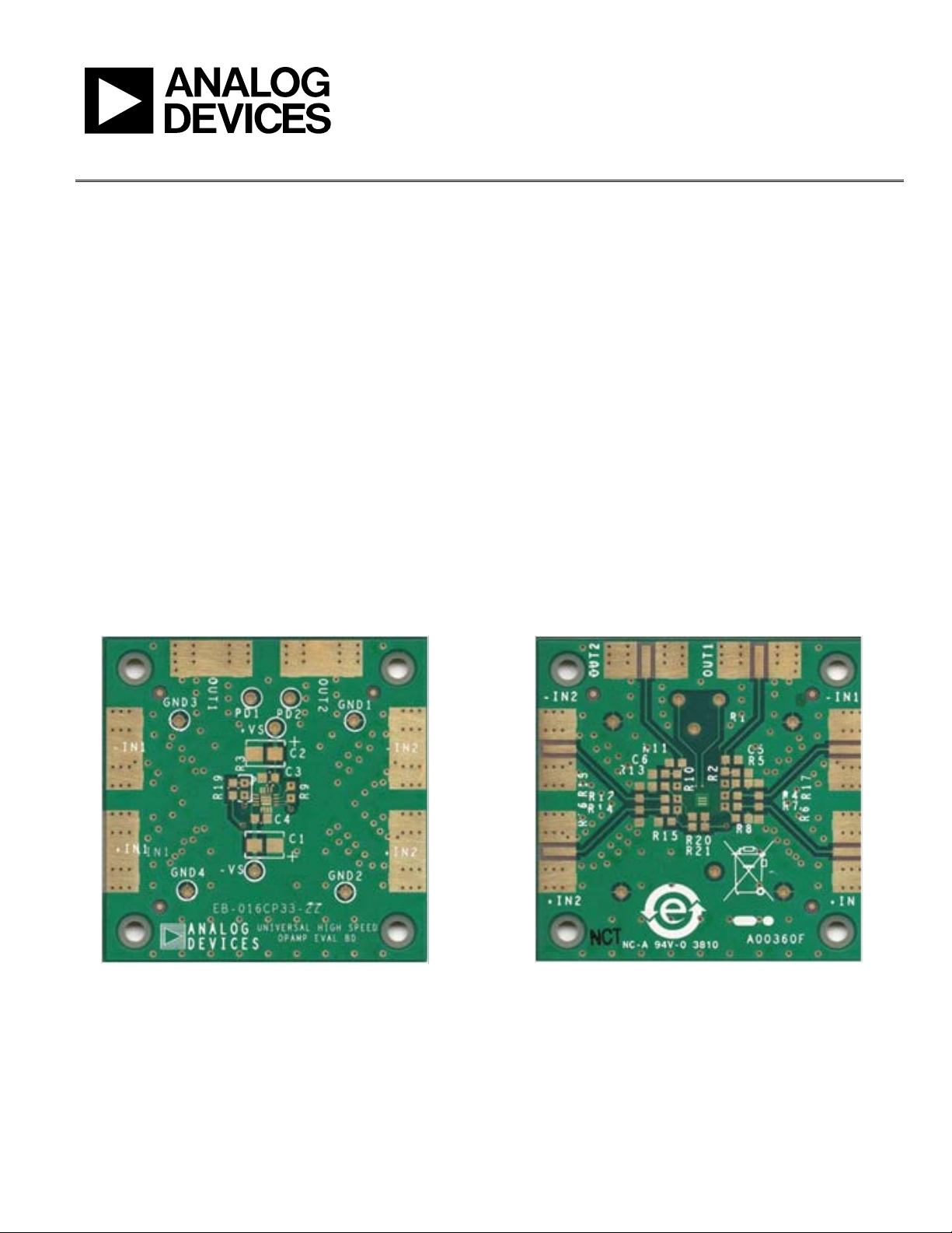
reduces time to market. Figure 1 and Figure 2 show the bare
evaluation board component and circuit sides.
The evaluation board is a 2-layer PCB that accepts SMA edge
mounted connectors on the inputs and outputs for efficient
connection to test equipment or other circuitry. The ground
plane, component placement, and supply bypassing are
designed to minimize parasitic inductances and capacitances.
The evaluation board components are primarily SMT 0805
case size, with the exception of the electrolytic bypass capacitors (C1 and C2), which are 3528 case size.
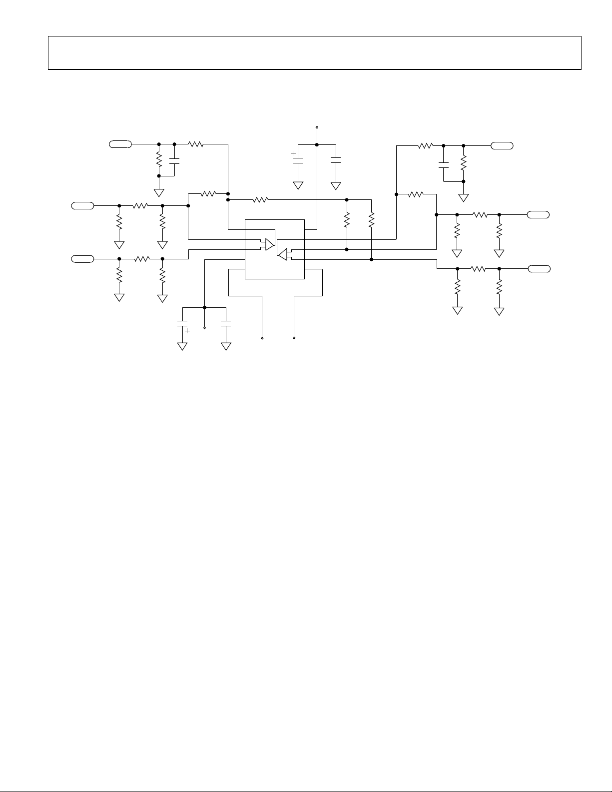
Figure 3 shows the evaluation board schematic. The evaluation
board assembly drawings and layout patterns are shown in
Figure 4 through Figure 7.
EVALUATION BOARD COMPONENT AND CIRCUIT SIDES
NOTES
1. THE EVALUATION BOARD SILKSCRE E N P ART NUMBER LABELING
ON YOUR BOARD M AY BE DIFFERENT FROM WHAT IS SHOWN HERE .
Figure 1. Component Side of Evaluation Board
NOTES
1. THE EVALUATION BOARD SILKSCRE E N P ART NUMBER LABELING
08145-101
ON YOUR BOARD M AY BE DIFFERENT FROM WHAT IS SHOWN HERE .
Figure 2. Circuit Side of Evaluation Board
08145-102
PLEASE SEE THE LAST PAGE FOR AN IMPORTANT
WARNING AND LEGAL TERMS AND CONDITIONS.
Rev. A | Page 1 of 8

UG-017 Evaluation Board User Guide
TABLE OF CONTENTS
Features .............................................................................................. 1
General Description ......................................................................... 1
Evaluation Board Component and Circuit Sides ......................... 1
Revision History ............................................................................... 2
REVISION HISTORY
6/11—Rev. 0 to Rev. A
Changes to Features and General Descriptions Sections ............ 1
Changes to Figure 1 .......................................................................... 1
Added Figure 2 .................................................................................. 1
Changes to Evaluation Board Schematic, Assembly Drawings,
and Layout Patterns ............................................................................ 3
Added Ordering Information Section .......................................... 6
2/10—Revision 0: Initial Version
Evaluation Board Schematics, Assembly Drawings and Layout
Patterns ...............................................................................................3
Ordering Information .......................................................................6
Bill of Materials ..............................................................................6
Rev. A | Page 2 of 8

Evaluation Board User Guide UG-017
14 13
16LFCSP3X3_B
AGND
AGND
AGND
AGND
AGND AGND
AGND AGND
AGND AGND
AGND
AGND
AGND
AGND
+IN2
–IN2
+IN1
–IN1
C5*
C6*
R2*
C3*
PD2/DIS2
PD1/DIS1
R15*
R3*
R12*
R14*
R13*
R9*
R10*
R8*
–VS
C4*
OUT2
+VS
1
2
3
4 9
10
11
12
Z1
R16*
R11*
R7*
R5*
R4*
R6*
*USER-DEFI NED VAL UE
R1*
10UF
C2
10UF
C1
OUT1
+VS
R17*
R18*
R19*
R20* R21*
08145-001
EVALUATION BOARD SCHEMATICS, ASSEMBLY DRAWINGS AND LAYOUT PATTERNS
Figure 3. Evaluation Board Schematic
Rev. A | Page 3 of 8

UG-017 Evaluation Board User Guide
08145-104
08145-105
Figure 4. Assembly Drawing, Component Side
Figure 5. Assembly Drawing, Circuit Si de
Rev. A | Page 4 of 8

Evaluation Board User Guide UG-017
08145-107
08145-106
Figure 6. Layout Pattern, Component Side
Figure 7. Layout Pattern, Circuit Side
Rev. A | Page 5 of 8

UG-017 Evaluation Board User Guide
ORDERING INFORMATION
BILL OF MATERIALS
Table 1.
Quantity Reference Designator Description Package
8 +VS, −VS, GND1, GND2, GND3, GND4, PD1, PD2 Test point TP
2 C1, C2 10 µF capacitor 3528
4 C3, C4, C5, C6 Capacitor, user defined C0805
1 DUT DEV, QFN16_3x3 16-lead LFCSP
6 +IN1, +IN2, −IN1, −IN2, OUT1, OUT2 SMA/SMT SMA/SMT
21 R1 to R21 Resistor, user defined R0805
Rev. A | Page 6 of 8

Evaluation Board User Guide UG-017
NOTES
Rev. A | Page 7 of 8

UG-017 Evaluation Board User Guide
signify your acceptance of the Agreement. This Agreement is made by and between you (“Customer”) and Analog Devices, Inc.
neer chips on the Evaluation Board. Customer shall inform ADI of any
ut not limited to the RoHS Directive. TERMINATION. ADI may terminate this Agreement at any time upon giving written notice
NOTES
ESD Caution
ESD (electrostatic discharge) sensitive device. Charged devices and circuit boards can discharge without detection. Although this product features patented or proprietary protection
circuitry, damage may occur on devices subjected to high e nergy ESD. Therefore, proper ESD precaution s should be taken to avoid per forma nce degra dation or loss of functionality.
Legal Terms and Conditions
By using the evaluation board discussed herein (together with any tools, components documentation or support materials, the “Evaluation Board”), you are agreeing to be bound by the terms a nd conditions
set forth below ( “Agreement ”) unless you have purchased the Evaluation Board, in which case the Analog Devices Standard Terms and Conditions of Sale shall govern. Do not u se the Evaluation Board until you
have read and agreed to the Agreement. Your use of the Evaluation Board shall
(“ADI”), with its principal place of business at One Technology Way, Norwood, MA 02062, USA. S ubject to the terms and conditions of the Agreement, ADI hereby grants to Customer a free, limited, personal,
temporary, non-exclusive, non-sublicensable, non-transferable license to use the Evaluation Board FOR EVALUATION PURPOSES ONLY. Customer understands and agrees that the Evaluation Board is provided
for the sole and exclusive purpose referenced above, and agrees not to use the Evaluation Board for any other purpose. Further more, the license granted is expressly made subject to the following additional
limitations: Customer shall not (i) rent, lease, display, sell, transfer, assign, sublicense, or distribute the Evaluation Board; and (ii) permit any Third Party to access the Evaluation Board. As used herein, the term
“Third Party ” includes any entity other than ADI, Customer, their employees, affiliates and in-house consultants. The Evaluation Board is NOT sold to Customer; all rights not expressly granted herein, including
ownership of the Evaluation Board, are reserved by ADI. CONFIDENTIALIT Y. This Agreement and the Evaluation Board shall all be considered the confidential and proprietary information of ADI. Customer may
not disclose or transfer any portion of the Evaluation Board to any other party for any reason. Upon discontinuation of use of the Evaluation Board or termination of this Agreement, Customer agrees to
promptly return the Evaluation Board to ADI. ADDITIONAL RESTRICTIONS. Customer may not disassemble, decompile or reverse engi
occurred damages or any modifications or alterations it makes to the Evaluation Board, including but not limited to soldering or any other activity that affects the material content of the Evaluation Board.
Modifications to the Evaluation Board must comply with applicable law, inclu ding b
to Customer. Customer agrees to return to ADI the Evaluation Board at that time. LIMITATION OF LIABILITY. THE EVALUATION BOARD PROVIDED HEREUNDER IS PROVIDED “AS IS” AND ADI MAKES NO
WARRANTIES OR REPRES ENTATIONS OF ANY KIND WITH RESPECT TO IT. ADI SPECIFICAL LY DISC LAIMS ANY REPRESENTATIONS, ENDORSEMENTS, GUA RANTEES, OR WARRANT IES, EXPRESS OR IMPLIED, RELATED
TO THE EVALUATION BOARD INCLUDING, BUT NOT LIMITED TO, THE IMPLIED WARRANTY OF MERCHANTABILITY, TITLE, FITNESS FOR A PARTICULAR PURPOSE OR NONINFRINGEMENT OF INTELLECTUAL
PROPERTY RIGHTS. IN NO EVENT WILL ADI AND ITS LICENSORS BE LIABLE FOR ANY INCIDENTAL, SPECIAL, INDIRECT, OR CONSEQUENTIAL DAMAGES RESULTING FROM CUSTOMER’S POSSESSION OR USE OF
THE EVALUAT ION BOARD, INCLUDING BUT NOT LIMI TED TO LOST PROFITS, DE LAY COSTS, LABOR COSTS OR LOSS OF GOODWI LL. ADI’S TOTAL LIA BILITY FROM AN Y AND ALL CAUSES S HALL BE LIMITE D TO THE
AMOUNT OF ONE HUNDRED US DOLLARS ($100.00). EXPORT. Customer agrees that it will not directly or indirec tly export the Evaluation Board to another country, and that it will comply with all applicable
United States federal laws and regulations relating to exports. GOVERNING LAW. This Agreement shall be governed by and construed in accordance with the substantive laws of the Commonwealth of
Massachusetts (excluding conflict of law rules). Any legal action regarding this Ag re ement will be heard in the state or federal courts having jurisdiction in Suffolk County, Massachusetts, and Customer hereby
submits to the personal jurisdiction and venue of such courts. The United Nations Convention on Contracts for the International Sale of Goods shall no t apply to this Agreement and is expressly disclaime d.
©2010–2011 Analog Devices, Inc. All rights reserved. Trademarks and
registered trademarks are the property of their respective owners.
UG08145-0-6/11(A)
Rev. A | Page 8 of 8
 Loading...