

Page 1
Low Power, Programmable
VPTAT
V+
TEMPERATURE
SENSOR &
VOLTAGE
REFERENCE
2.5V
SENSOR
1
2
3
4
8
7
6
5
HYSTERESIS
GENERATOR
WINDOW
COMPARATOR
R1
TMP01
VREF
SET
HIGH
SET
LOW
GND
R2
R3
UNDER
OVER
a
FEATURES
–558C to +1258C (–678F to +2578F) Operation
61.08C Accuracy Over Temperature (typ)
Temperature-Proportional Voltage Output
User Programmable Temperature Trip Points
User Programmable Hysteresis
20 mA Open Collector Trip Point Outputs
TTL/CMOS Compatible
Single-Supply Operation (4.5 V to 13.2 V)
Low Cost 8-Pin DIP and SO Packages
APPLICATIONS
Over/Under Temperature Sensor and Alarm
Board Level Temperature Sensing
Temperature Controllers
Electronic Thermostats
Thermal Protection
HVAC Systems
Industrial Process Control
Remote Sensors
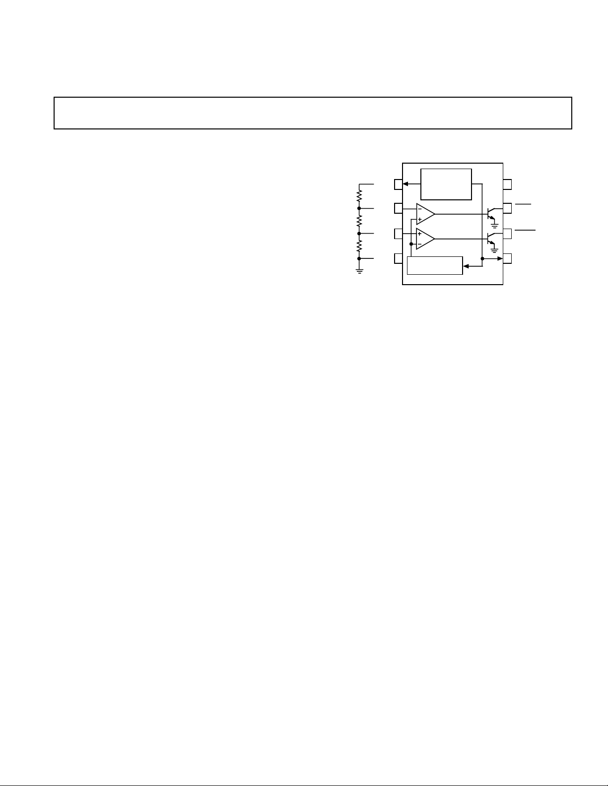
GENERAL DESCRIPTION
The TMP01 is a temperature sensor which generates a voltage
output proportional to absolute temperature and a control signal
from one of two outputs when the device is either above or
below a specific temperature range. Both the high/low temperature trip points and hysteresis (overshoot) band are determined
by user-selected external resistors. For high volume production,
these resistors are available on-board.
The TMP01 consists of a bandgap voltage reference combined
with a pair of matched comparators. The reference provides
both a constant 2.5 V output and a voltage proportional to absolute temperature (VPTAT) which has a precise temperature coefficient of 5 mV/K and is 1.49 V (nominal) at +25°C. The
comparators compare VPTAT with the externally set temperature trip points and generate an open-collector output signal
when one of their respective thresholds has been exceeded.
Temperature Controller
TMP01*
FUNCTIONAL BLOCK DIAGRAM
Hysteresis is also programmed by the external resistor chain and
is determined by the total current drawn out of the 2.5 V reference. This current is mirrored and used to generate a hysteresis
offset voltage of the appropriate polarity after a comparator has
been tripped. The comparators are connected in parallel, which
guarantees that there is no hysteresis overlap and eliminates
erratic transitions between adjacent trip zones.
The TMP01 utilizes proprietary thin-film resistors in conjunction with production laser trimming to maintain a temperature
accuracy of ±1°C (typ) over the rated temperature range, with
excellent linearity. The open-collector outputs are capable of
sinking 20 mA, enabling the TMP01 to drive control relays directly. Operating from a +5 V supply, quiescent current is only
500 µA (max).
The TMP01 is available in the low cost 8-pin epoxy mini-DIP
and SO (small outline) packages, and in die form.
*Protected by U.S. Patent No. 5,195,827.
REV. C
Information furnished by Analog Devices is believed to be accurate and
reliable. However, no responsibility is assumed by Analog Devices for its
use, nor for any infringements of patents or other rights of third parties
which may result from its use. No license is granted by implication or
otherwise under any patent or patent rights of Analog Devices.
© Analog Devices, Inc., 1995
One Technology Way, P.O. Box 9106, Norwood. MA 02062-9106, U.S.A.
Tel: 617/329-4700 Fax: 617/326-8703
Page 2

TMP01EP/FP, TMP01ES/FS–SPECIFICATIONS
Plastic DIP and Surface Mount Packages
(V+ = +5 V, GND = O V, –408C ≤ TA ≤ +858C unless otherwise noted)
Parameter Symbol Conditions Min Typ Max Units
INPUTS SET HIGH, SET LOW
Offset Voltage V
Offset Voltage Drift TCV
Input Bias Current, “E” I
Input Bias Current, “F” I
OUTPUT VPTAT
1
OS
OS
B
B
0.25 mV
3 µV/°C
25 50 nA
25 100 nA
Output Voltage VPTAT TA = +25°C, No Load 1.49 V
Scale Factor TC
Temperature Accuracy, “E” T
Temperature Accuracy, “F” T
VPTAT
= +25°C, No Load –1.5 ±0.5 1.5 °C
A
= +25°C, No Load –3 ±1.0 3 °C
A
Temperature Accuracy, “E” 10°C < T
Temperature Accuracy, “F” 10°C < T
Temperature Accuracy, “E” –40°C < T
Temperature Accuracy, “F” –40°C < T
Temperature Accuracy, “E” –55°C < T
Temperature Accuracy, “F” –55°C < T
< 40°C, No Load ±0.75 °C
A
< 40°C, No Load ±1.5 °C
A
< 85°C, No Load –3.0 ±1 3.0 °C
A
< 85°C, No Load –5.0 ±2 5.0 °C
A
< 125°C, No Load ±1.5 °C
A
< 125°C, No Load ±2.5 °C
A
5 mV/K
Repeatability Error ∆VPTAT Note 4 0.25 Degree
Long Term Drift Error Notes 2 and 6 0.25 0.5 Degree
Power Supply Rejection Ratio PSRR TA = +25°C, 4.5 V ≤ V+ ≤ 13.2 V ±0.02 ±0.1 %/V
OUTPUT VREF
Output Voltage, “E” VREF T
Output Voltage, “F” VREF T
Output Voltage, “E” VREF –40°C < T
Output Voltage, “F” VREF –40°C < T
Output Voltage, “E” VREF –55°C < T
Output Voltage, “F” VREF –55°C < T
Drift TC
VREF
= +25°C, No Load 2.495 2.500 2.505 V
A
= +25°C, No Load 2.490 2.500 2.510 V
A
< 85°C, No Load 2.490 2.500 2.510 V
A
< 85°C, No Load 2.485 2.500 2.515 V
A
< 125°C, No Load 2.5 ± 0.01 V
A
< 125°C, No Load 2.5 ± 0.015 V
A
–10 ppm/°C
Line Regulation 4.5 V ≤ V+ ≤ 13.2 V ±0.01 ±0.05 %/V
Load Regulation 10 µA ≤ I
Output Current, Zero Hysteresis I
Hysteresis Current Scale Factor SF
VREF
HYS
(Note 1) 5.0 µA/°C
≤ 500 µA ±0.1 ±0.25 %/mA
VREF
7 µA
Turn-On Settling Time To Rated Accuracy 25 µs
OPEN-COLLECTOR OUTPUTS OVER, UNDER
I
Output Low Voltage V
Output Low Voltage V
Output Leakage Current I
Fall Time t
OL
OL
OH
HL
= 1.6 mA 0.25 0.4 V
SINK
I
= 20 mA 0.6 V
SINK
V+ = 12 V 1 100 µA
See Test Load 40 ns
POWER SUPPLY
Supply Range V+ 4.5 13.2 V
Supply Current I
Supply Current I
Power Dissipation P
NOTES
1
K = °C + 273.15.
2
Guaranteed but not tested.
3
Does not consider errors caused by heating due to dissipation of output load currents.
4
Maximum deviation between +25°C readings after temperature cycling between –55°C and +125°C.
5
Typical values indicate performance measured at TA = +25°C.
6
Observed in a group sample over an accelerated life test of 500 hours at 150°C.
Specifications subject to change without notice.
SY
SY
DISS
Unloaded, +V = 5 V 400 500 µA
Unloaded, +V = 13.2 V 450 800 µA
+V = 5 V 2.0 2.5 mW
Test Load
V+
1kΩ
20pF
–2–
REV. C
Page 3

TMP01
TO-99 Metal Can Package (V+ = +5 V, GND = O V, –408C ≤ TA ≤ +858C
TMP01FJ–SPECIFICA TIONS
Parameter Symbol Conditions Min Typ Max Units
INPUTS SET HIGH, SET LOW
Offset Voltage V
Offset Voltage Drift TCV
Input Bias Current, “F” I
OUTPUT VPTAT
1
Output Voltage VPTAT TA = +25°C, No Load 1.49 V
Scale Factor TC
Temperature Accuracy, “F” T
Temperature Accuracy, “F” 10°C < T
Temperature Accuracy, “F” –40°C < T
Temperature Accuracy, “F” –55°C < T
Repeatability Error ∆VPTAT Note 4 0.25 Degree
Long Term Drift Error Notes 2 and 6 0.25 0.5 Degree
Power Supply Rejection Ratio PSRR TA = +25°C, 4.5 V ≤ V+ ≤ 13.2 V ±0.02 ±0.1 %/V
OUTPUT VREF
Output Voltage, “F” VREF T
Output Voltage, “F” VREF –40°C < T
Output Voltage, “F” VREF –55°C < T
Drift TC
Line Regulation 4.5 V ≤ V+ ≤ 13.2 V ±0.01 ±0.05 %/V
Load Regulation 10 µA ≤ I
Output Current, Zero Hysteresis I
Hysteresis Current Scale Factor SF
Turn-On Settling Time To Rated Accuracy 25 µs
OPEN-COLLECTOR OUTPUTS OVER, UNDER
Output Low Voltage V
Output Low Voltage V
Output Leakage Current I
Fall Time t
POWER SUPPLY
Supply Range V+ 4.5 13.2 V
Supply Current I
Supply Current I
Power Dissipation P
NOTES
1
K = °C + 273.15.
2
Guaranteed but not tested.
3
Does not consider errors caused by heating due to dissipation of output load currents.
4
Maximum deviation between +25°C readings after temperature cycling between –55°C and +125°C.
5
Typical values indicate performance measured at TA = +25°C.
6
Observed in a group sample over an accelerated life test of 500 hours at 150°C.
Specifications subject to change without notice.
OS
OS
B
VPTAT
VREF
VREF
HYS
OL
OL
OH
HL
SY
SY
DISS
unless otherwise noted)
0.25 mV
3 µV/°C
25 100 nA
5 mV/K
= +25°C, No Load –3 ±1.0 3 °C
A
= +25°C, No Load 2.490 2.500 2.510 V
A
< 40°C, No Load ±1.5 °C
A
< 85°C, No Load –5.0 ±2 5.0 °C
A
< 125°C, No Load ±2.5 °C
A
< 85°C, No Load 2.480 2.500 2.520 V
A
< 125°C, No Load 2.5 ± 0.015 V
A
–10 ppm/°C
≤ 500 µA ±0.1 ±0.25 %/mA
VREF
7 µA
(Note 1) 5.0 µA/°C
I
= 1.6 mA 0.25 0.4 V
SINK
I
= 20 mA 0.6 V
SINK
V+ = 12 V 1 100 µA
See Test Load, Note 2 40 ns
Unloaded, +V = 5 V 400 500 µA
Unloaded, +V = 13.2 V 450 800 µA
+V = 5 V 2.0 2.5 mW
REV. C
–3–
Page 4
TMP01
W AFER TEST LIMITS
(VDD = +5.0 V, GND = 0 V, TA = +258C, unless otherwise noted)
Parameter Symbol Conditions Min Typ Max Units
INPUTS SET HIGH, SET LOW
Input Bias Current I
B
100 nA
OUTPUT VPTAT
Temperature Accuracy TA = +25°C, No Load 1.5 °C
OUTPUT VREF
Nominal Value VREF T
= +25°C, No Load 2.490 2.510 V
A
Line Regulation 4.5 V ≤ V+ ≤ 13.2 V ±0.05 %/V
Load Regulation 10 µA ≤ I
≤ 500 µA ±0.25 %/mA
VREF
OPEN-COLLECTOR OUTPUTS OVER, UNDER
Output Low Voltage V
Output Low Voltage V
Output Leakage Current I
OL
OL
OH
I
= 1.6 mA 0.4 mV
SINK
I
= 20 mA 1.0 V
SINK
100 µA
POWER SUPPLY
Supply Range V+ 4.5 13.2 V
Supply Current I
NOTES
Electrical tests are performed at wafer probe to the limits shown. Due to variations in assembly methods and normal yield loss, yield after packaging is not guaranteed
for standard product dice. Consult factory to negotiate specifications based on dice lot qualification through sample lot assembly and testing.
SY
Unloaded 600 µA
DICE CHARACTERISTICS
Die Size 0.078 × 0.071 inch, 5,538 sq. mils
(1.98 × 1.80 mm, 3.57 sq. mm)
Transistor Count: 105
8
1
7
2 3
6
5
1. VREF
2. SETHIGH
3. SETLOW
4. GND (TWO PLACES)
(CONNECTED TO SUBSTRATE)
5. VPTAT
4
4
6. UNDER
7. OVER
8. V+
For additional DICE ordering information, refer to databook.
–4–
REV. C
Page 5
TMP01
ABSOLUTE MAXIMUM RATINGS
Maximum Supply Voltage . . . . . . . . . . . . . . . . –0.3 V to +15 V
Maximum Input Voltage
(SETHIGH, SETLOW) . . . . . . . . .–0.3 V to [(V+) +0.3 V]
Maximum Output Current (VREF, VPTAT) . . . . . . . . . 2 mA
Maximum Output Current (Open Collector Outputs) . . 50 mA
Maximum Output Voltage (Open Collector Outputs) . . . .15 V
Operating Temperature Range . . . . . . . . . . . .–55°C to +150°C
Dice Junction Temperature . . . . . . . . . . . . . . . . . . . . . +150°C
Storage Temperature Range . . . . . . . . . . . . – 65°C to +150°C
Lead Temperature (Soldering, 60 sec) . . . . . . . . . . . . . +300°C
Package Type θ
8-Pin Plastic DIP (P) 103
8-Lead SOIC (S) 158
8-Lead TO-99 Can (J) 150
NOTES
1
θJA is specified for device in socket (worst case conditions).
2
θJA is specified for device mounted on PCB.
JA
1
2
1
θ
JC
Units
43 °C/W
43 °C/W
18 °C/W
CAUTION
1. Stresses above those listed under “Absolute Maximum Rat-
ings” may cause permanent damage to the device. This is a
stress rating only and functional operation at or above this
specification is not implied. Exposure to the above maximum
rating conditions for extended periods may affect device
reliability.
2. Digital inputs and outputs are protected, however, permanent
damage may occur on unprotected units from high energy
electrostatic fields. Keep units in conductive foam or packaging at all times until ready to use. Use proper antistatic handling procedures.
3. Remove power before inserting or removing units from their
sockets.
ORDERING GUIDE
Temperature Package Package
Model/Grade Range
l
Description Option
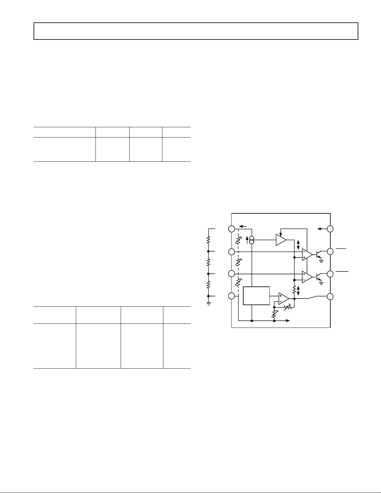
GENERAL DESCRIPTION
The TMP01 is a very linear voltage-output temperature sensor,
with a window comparator that can be programmed by the user
to activate one of two open-collector outputs when a predetermined temperature setpoint voltage has been exceeded. A low
drift voltage reference is available for setpoint programming.
The temperature sensor is basically a very accurately temperature compensated, bandgap-type voltage reference with a buffered output voltage proportional to absolute temperature
(VPTAT), accurately trimmed to a scale factor of 5 mV/K. See
the Applications Information following.
The low drift 2.5 V reference output VREF is easily divided externally with fixed resistors or potentiometers to accurately establish the programmed heat/cool setpoints, independent of
temperature. Alternatively, the setpoint voltages can be supplied
by other ground referenced voltage sources such as userprogrammed DACs or controllers. The high and low setpoint
voltages are compared to the temperature sensor voltage, thus
creating a two-temperature thermostat function. In addition,
the total output current of the reference (I
) determines the
VREF
magnitude of the temperature hysteresis band. The open collector outputs of the comparators can be used to control a wide variety of devices.
HYSTERESIS
VREF
SET
HIGH
SET
LOW
GND
2
3
4
CURRENT
VOLTAGE
REFERENCE
SENSOR
CURRENT
MIRROR
AND
ENABLE
WINDOW
COMPARATOR
1kΩ
I
HYS
HYSTERESIS
VOLTAGE
TEMPERATURE
OUTPUT
TMP01
81
7
6
5
V+
OVER
UNDER
VPTAT
TMP01EP XIND Plastic DIP N-8
TMP01FP XIND Plastic DIP N-8
TMP01ES XIND SOIC SO-8
TMP01FS XIND SOIC SO-8
TMP01FJ
2
XIND TO-99 Can H-08A
TMP01GBC +25°C Die
NOTES
1
XIND = –40°C to +85°C.
2
Consult factory for availability of MIL/883 version in TO-99 can.
REV. C
Figure 1. Detailed Block Diagram
–5–
Page 6

TMP01
Temperature Hysteresis
The temperature hysteresis is the number of degrees beyond the
original setpoint temperature that must be sensed by the TMP01
before the setpoint comparator will be reset and the output disabled. Figure 2 shows the hysteresis profile. The hysteresis is
programmed by the user by setting a specific load on the reference voltage output VREF. This output current I
VREF
is also
called the hysteresis current, which is mirrored internally and
fed to a buffer with an analog switch.
HYSTERESIS
HIGH
T
SETHIGH
OUTPUT
VOLTAGE
OVER, UNDER
LO
HI
HYSTERESIS
LOW
T
SETLOW
HYSTERESIS HIGH =
HYSTERESIS LOW
TEMPERATURE
Figure 2. TMP01 Hysteresis Profile
After a temperature setpoint has been exceeded and a comparator tripped, the buffer output is enabled. The output is a current of the appropriate polarity which generates a hysteresis
offset voltage across an internal 1000 Ω resistor at the comparator input. The comparator output remains “on” until the voltage at the comparator input, now equal to the temperature
sensor voltage VPTAT summed with the hysteresis offset, has
returned to the programmed setpoint voltage. The comparator
then returns LOW, deactivating the open-collector output and
disabling the hysteresis current buffer output. The scale factor
for the programmed hysteresis current is:
I
HYS
= I
= 5 µA/°C + 7 µA
VREF
Thus since VREF = 2.5 V, with a reference load resistance of
357 kΩ or greater (output current 7 µA or less), the temperature
setpoint hysteresis will be zero degrees. See the temperature
programming discussion below. Larger values of load resistance
will only decrease the output current below 7 µA and will have
no effect on the operation of the device. The amount of hysteresis is determined by selecting a value of load resistance for
VREF, as shown below.
Programming the TMP01
In the basic fixed-setpoint application utilizing a simple resistor
ladder voltage divider, the desired temperature setpoints are
programmed in the following sequence:
1. Select the desired hysteresis temperature.
2. Calculate the hysteresis current I
VREF
.
3. Select the desired setpoint temperatures.
4. Calculate the individual resistor divider ladder values needed
to develop the desired comparator setpoint voltages at
SETHIGH and SETLOW.
The hysteresis current is readily calculated, as shown. For
example, for 2 degrees of hysteresis, I
setpoint voltages V
SETHIGH
and V
SETLOW
= 17 µA. Next, the
VREF
are determined using
the VPTAT scale factor of 5 mV/K = 5 mV/(°C + 273.15),
which is 1.49 V for +25°C. We then calculate the divider resistors, based on those setpoints. The equations used to calculate
the resistors are:
V
V
R1 (kΩ) = (V
R2 (kΩ) = (V
R3 (kΩ) = V
SETHIGH
SETLOW
(V
(V
SETHIGH
= (T
SETHIGH
= (T
SETLOW
– V
VREF
= (2.5 V – V
SETHIGH
SETLOW/IVREF
– V
VREF
SETHIGH
– V
SETLOW
V
SETLOW
+ 273.15)(5 mV/°C)
+ 273.15) (5 mV/°C)
)/I
)/I
VREF
VREF
)/I
I
VREF
=
VREF
1
2
3
4
V
VREF
)/I
)/I
/I
– V
VREF
V
VREF
VREF
SETHIGH
SETHIGH
SETLOW
= 2.5V
= R1
SETHIGH
= R2
V
SETLOW
= R3
GND
TMP01
8
7
6
5
V+
OVER
UNDER
VPTAT
Figure 3. TMP01 Setpoint Programming
The total R1 + R2 + R3 is equal to the load resistance needed
to draw the desired hysteresis current from the reference, or
I
.
VREF
The formulas shown above are also helpful in understanding the
calculation of temperature setpoint voltages in circuits other
than the standard two-temperature thermostat. If a setpoint
function is not needed, the appropriate comparator should be
disabled. SETHIGH can be disabled by tying it to V+, SETLOW by tying it to GND. Either output can be left unconnected.
218 248 273 298 323 348 373 398
K
–55 –25
–18
0 25 50 75 100 125
°C
–67 –25 0 32 50 77 100 150 200 212 257
°F
1.09 1.24 1.365 1.49 1.615 1.74 1.865 1.99
VPTAT
Figure 4. Temperature—VPTAT Scale
–6–
REV. C
Page 7

TMP01
Understanding Error Sources
The accuracy of the VPTAT sensor output is well characterized
and specified, however preserving this accuracy in a heating or
cooling control system requires some attention to minimizing
the various potential error sources. The internal sources of
setpoint programming error include the initial tolerances and
temperature drifts of the reference voltage VREF, the setpoint
comparator input offset voltage and bias current, and the hysteresis current scale factor. When evaluating setpoint programming errors, remember that any VREF error contribution at the
comparator inputs is reduced by the resistor divider ratios. The
comparator input bias current (inputs SETHIGH, SETLOW)
drops to less than 1 nA (typ) when the comparator is tripped.
This can account for some setpoint voltage error, equal to the
change in bias current times the effective setpoint divider ladder
resistance to ground.
The thermal mass of the TMP01 package and the degree of
thermal coupling to the surrounding circuitry are the largest
factors in determining the rate of thermal settling, which ultimately determines the rate at which the desired temperature
measurement accuracy may be reached. Thus, one must allow
sufficient time for the device to reach the final temperature.
The typical thermal time constant for the plastic package is
approximately 140 seconds in still air! Therefore, to reach the
final temperature accuracy within 1%, for a temperature change
of 60 degrees, a settling time of 5 time constants, or 12 minutes, is necessary.
The setpoint comparator input offset voltage and zero hysteresis current affect setpoint error. While the 7 µA zero hysteresis
current allows the user to program the TMP01 with moderate
resistor divider values, it does vary somewhat from device to device, causing slight variations in the actual hysteresis obtained
in practice. Comparator input offset directly impacts the programmed setpoint voltage and thus the resulting hysteresis
band, and must be included in error calculations.
External error sources to consider are the accuracy of the programming resistors, grounding error voltages, and the overall
problem of thermal gradients. The accuracy of the external
programming resistors directly impacts the resulting setpoint
accuracy. Thus in fixed-temperature applications the user
should select resistor tolerances appropriate to the desired
programming accuracy. Resistor temperature drift must be
taken into account also. This effect can be minimized by selecting good quality components, and by keeping all components in
close thermal proximity. Applications requiring high measurement accuracy require great attention to detail regarding
thermal gradients. Careful circuit board layout, component
placement, and protection from stray air currents are necessary
to minimize common thermal error sources.
Also, the user should take care to keep the bottom of the
setpoint programming divider ladder as close to GND (Pin 4)
as possible to minimize errors due to IR voltage drops and coupling of external noise sources. In any case, a 0.1 µF capacitor
for power supply bypassing is always recommended at the chip.
Safety Considerations In Heating And Cooling System Design
Designers should anticipate potential system fault conditions
which may result in significant safety hazards which are outside
the control of and cannot be corrected by the TMP01-based
circuit. Governmental and industrial regulations regarding
safety requirements and standards for such designs should be
observed where applicable.
REV. C
550
525
500
475
+125°C
450
425
SUPPLY CURRENT – µA
400
375
350
+85°C
–55°C
+25°C
–40°C
SUPPLY VOLTAGE – Volts
Figure 5. Supply Current vs. Supply Voltage
5.0
4.5
4.0
3.5
MINIMUM SUPPLY VOLTAGE – Volts
3.0
20501510
–75 125–50 1007550250–25
TEMPERATURE – °C
Figure 6. Minimum Supply Voltage vs. Temperature
–7–
Page 8

TMP01
+2.0
+1.5
+1.0
C
°
+0.5
0
–0.5
VPTAT ERROR –
–1.0
–1.5
–3.0
–75 125–50 1007550250–25
TEMPERATURE –
V+ = +5V
°
C
Figure 7. VPTAT Accuracy vs. Temperature
2.508
2.506
2.504
2.502
VREF – Volts
2.500
V+ = +5V
2.510
2.508
CURVES NOT NORMALIZED
2.506
EXTRAPOLATED FROM OPERATING LIFE DATA
2.504
2.502
2.500
2.498
VREF – Volts
2.496
2.494
2.492
2.490
T = HOURS OF OPERATION AT 125°C; V+ = +5V
X + 3σ
X
X – 3σ
10002000 800400 600
Figure 10. VREF Long Term Drift Accelerated by Burn-In
100
80
60
40
PSRR – dB
20
V+ = +5V
I
= 10µA
VREF
2.498
2.496
–75 125–50 1007550250–25
TEMPERATURE – °C
Figure 8. VREF Accuracy vs. Temperature
6.0
VC = +15V
V+ = +5V
5.0
TA = +25°C
4.0
3.0
– Volts
CE
V
2.0
1.0
0
IC – mA
Figure 9. Open-Collector Output (
tion Voltage vs. Output Current
OVER, UNDER
50100 403020
) Satura-
0
–20
100
1k 1M100k10k
FREQUENCY – Hz
Figure 11. VREF Power Supply Rejection vs. Frequency
1.0
0.1
OFFSET VOLTAGE – mV
V+ = +5V
I
= 7.5µA
VREF
0.01
–75 –50 1251007550250–25
TEMPERATURE – °C
Figure 12. Set High, Set Low Input Offset Voltage vs.
Temperature
–8–
REV. C
Page 9

8
7.26.2 7
6.8
6.66.4 87.87.67.4
REFERENCE CURRENT – µA
NUMBER OF DEVICES
10
0
2
1
4
3
5
6
7
8
9
V+ = +5V
T
A
= +25°C
7
6
5
4
3
NUMBER OF DEVICES
2
1
0
–0.32
–0.4 –0.24
OFFSET – mV
V+ = +5V
= +25°C
T
A
I
VREF
0–0.08–0.16 0.160.08
TMP01
= 5µA
APPLICATIONS INFORMATION
Self-Heating Effects
In some applications the user should consider the effects of selfheating due to the power dissipated by the open-collector outputs, which are capable of sinking 20 mA continuously. Under full
load, the TMP01 open-collector output device is dissipating
which in a surface-mount SO package accounts for a temperature increase due to self-heating of
This will of course directly affect the accuracy of the TMP01
and will for example cause the device to switch the heating output “OFF” 2 degrees early. Alternatively, bonding the same
package to a moderate heatsink limits the self-heating effect to
approximately
which is a much more tolerable error in most systems. The
VREF and VPTAT outputs are also capable of delivering sufficient current to contribute heating effects and should not be
ignored.
Buffering the Voltage Reference
As mentioned before, the reference output VREF is used to generate the temperature setpoint programming voltages for the
TMP01 and also is used to determine the hysteresis temperature
band by the reference load current I
buffer amplifier is typically capable of 500 µA output drive into
as much as 50 pF load (max). Exceeding this load will affect the
accuracy of the reference voltage, could cause thermal sensing
errors due to dissipation, and may induce oscillations. Selection
of a low drift buffer functioning as a voltage follower with high
input impedance will ensure optimal reference accuracy, and
will not affect the programmed hysteresis current. Amplifiers
which offer the low drift, low power consumption, and low cost
appropriate to this application include the OP295, and members
of the OP90, OP97, OP177 families, and others as shown in the
following applications circuits.
REV. C
Figure 13. Comparator Input Offset Distribution
P
= 0.6 V × .020A = 12 mW
DISS
∆T = P
∆T = P
× θJA = .012 W × 158°C/W = 1.9°C.
DISS
× θJC = .012 W × 43°C/W = 0.52°C.
DISS
. The on-board output
VREF
Figure 14. Zero Hysteresis Current Distribution
With excellent drift and noise characteristics, VREF offers a
good voltage reference for data acquisition and transducer excitation applications as well. Output drift is typically better than
–10 ppm/°C, with 315 nV/√
Hz (typ) noise spectral density at
1 kHz.
Preserving Accuracy Over Wide Temperature Range
Operation
The TMP01 is unique in offering both a wide-range temperature
sensor and the associated detection circuitry needed to implement a complete thermostatic control function in one monolithic device. While the voltage reference, setpoint comparators,
and output buffer amplifiers have been carefully compensated to
maintain accuracy over the specified temperature range, the user
has an additional task in maintaining the accuracy over wide operating temperature ranges in this application. Since the TMP01
is both sensor and control circuit, in many applications it is possible that the external components used to program and interface the device may be subjected to the same temperature
extremes. Thus it may be necessary to locate components in
close thermal proximity to minimize large temperature differentials, and to account for thermal drift errors where appropriate,
such as resistor matching tempcos, amplifier error drift, and
the like. Circuit design with the TMP01 requires a slightly different perspective regarding the thermal behavior of electronic
components.
Thermal Response Time
The time required for a temperature sensor to settle to a specified accuracy is a function of the thermal mass of the sensor,
and the thermal conductivity between the sensor and the object
being sensed. Thermal mass is often considered equivalent to
capacitance. Thermal conductivity is commonly specified using
the symbol Q, and can be thought of as the reciprocal of thermal
resistance. It is commonly specified in units of degrees per watt
of power transferred across the thermal joint. Thus, the time required for the TMP01 to settle to the desired accuracy is dependent on the package selected, the thermal contact established in
that particular application, and the equivalent power of the heat
source. In most applications, the settling time is probably best
determined empirically.
–9–
Page 10

TMP01
Switching Loads With The Open-Collector Outputs
In many temperature sensing and control applications some type
of switching is required. Whether it be to turn on a heater when
the temperature goes below a minimum value or to turn off a
motor that is overheating, the open-collector outputs Over and
Under can be used. For the majority of applications, the switches
used need to handle large currents on the order of 1 amp and
above. Because the TMP01 is accurately measuring temperature, the open-collector outputs should handle less than 20 mA
of current to minimize self-heating. Clearly, the Over-temp and
Under-temp outputs should not drive the equipment directly.
Instead, an external switching device is required to handle the
large currents. Some examples of these are relays, power
MOSFETs, thyristors, IGBTs, and Darlingtons.
Figure 15 shows a variety of circuits where the TMP01 controls
a switch. The main consideration in these circuits, such as the
relay in Figure 15a, is the current required to activate the
switch.
+12V
TEMPERATURE
VREF
1
R1
2
R2
3
R3
4
SENSOR &
VOLTAGE
REFERENCE
WINDOW
COMPARATOR
HYSTERESIS
GENERATOR
VPTAT
TMP01
8
IN4001
OR EQUIV.
7
6
5
2604-12-311
COTO
MOTOR
SHUTDOWN
Figure 15a. Reed Relay Drive
It is important to check the particular relay you choose to ensure
that the current needed to activate the coil does not exceed the
TMP01’s recommended output current of 20 mA. This is easily
determined by dividing the relay coil voltage by the specified
coil resistance. Keep in mind that the inductance of the relay
will create large voltage spikes that can damage the TMP01 output unless protected by a commutation diode across the coil, as
shown. The relay shown has a contact rating of 10 watts maximum. If a relay capable of handling more power is desired, the
larger contacts will probably require a commensurately larger
coil, with lower coil resistance and thus higher trigger current.
As the contact power handling capability increases, so does the
current needed for the coil. In some cases an external driving
transistor should be used to remove the current load on the
TMP01 as explained in the next section.
Power FETs are popular for handling a variety of high current
DC loads. Figure 15b shows the TMP01 driving a p-channel
MOSFET transistor for a simple heater circuit. When the output transistor turns on, the gate of the MOSFET is pulled down
to approximately 0.6 V, turning it on. For most MOSFETs a
gate-to-source voltage or Vgs on the order of –2 V to –5 V is sufficient to turn the device on. Figure 15c shows a similar circuit
for turning on an n-channel MOSFET, except that now the gate
to source voltage is positive. Because of this reason an external
transistor must be used as an inverter so that the MOSFET will
turn on when the “Under Temp” output pulls down.
TEMPERATURE
1
R1
2
R2
3
R3
4
VREF
SENSOR &
VOLTAGE
REFERENCE
WINDOW
COMPARATOR
HYSTERESIS
GENERATOR
NC = NO CONNECT
VPTAT
TMP01
V+
8
2.4kΩ (12V)
1.2kΩ (6V)
5%
7
NC
6
NC
5
IRFR9024
OR EQUIV.
HEATING
ELEMENT
Figure 15b. Driving a P-Channel MOSFET
TEMPERATURE
R1
R2
R3
VREF
1
2
3
4
NC = NO CONNECT
SENSOR &
VOLTAGE
REFERENCE
WINDOW
COMPARATOR
HYSTERESIS
GENERATOR
VPTAT
TMP01
V+
8
7
NC
6
NC
5
4.7kΩ 4.7kΩ
2N1711
HEATING
ELEMENT
IRF130
Figure 15c. Driving a N-Channel MOSFET
Isolated Gate Bipolar Transistors (IGBT) combine many of the
benefits of power MOSFETs with bipolar transistors, and are
used for a variety of high power applications. Because IGBTs
have a gate similar to MOSFETs, turning on and off the devices
is relatively simple as shown in Figure 15d. The turn on voltage
for the IGBT shown (IRGBC40S) is between 3.0 and 5.5 volts.
This part has a continuous collector current rating of 50 A and a
maximum collector to emitter voltage of 600 V, enabling it to
work in very demanding applications.
TEMPERATURE
R1
R2
R3
VREF
1
2
3
4
NC = NO CONNECT
SENSOR &
VOLTAGE
REFERENCE
WINDOW
COMPARATOR
HYSTERESIS
GENERATOR
VPTAT
TMP01
V+
8
7
NC
6
NC
5
4.7kΩ 4.7kΩ
2N1711
MOTOR
CONTROL
IRGBC40S
Figure 15d. Driving an IGBT
–10–
REV. C
Page 11

TMP01
Q1
Q2
2N1711
V+
R1
R2
R3
4.7kΩ
TEMPERATURE
SENSOR &
VOLTAGE
REFERENCE
1
2
3
4
HYSTERESIS
GENERATOR
WINDOW
COMPARATOR
TMP01
VPTAT
VREF
7
8
5
6
I
C
4.7kΩ
2N1711
The last class of high power devices discussed here are Thyristors, which includes SCRs and Triacs. Triacs are a useful alternative to relays for switching ac line voltages. The 2N6073A
shown in Figure 15e is rated to handle 4A (rms). The
optoisolated MOC3011. Triac shown features excellent electrical isolation from the noisy ac line and complete control over
the high power Triac with only a few additional components.
TEMPERATURE
1
R1
2
R2
3
R3
4
VREF
SENSOR &
VOLTAGE
REFERENCE
WINDOW
COMPARATOR
HYSTERESIS
GENERATOR
NC = NO CONNECT
VPTAT
TMP01
V+ = 5V
8
300Ω
7
NC
1
2
6
5
MOC3011
34
NC
LOAD
150Ω
6
5
2N6073A
AC
Figure 15e. Controlling the 2N6073A Triac
High Current Switching
As mentioned above, internal dissipation due to large loads on
the TMP01 outputs will cause some temperature error due to
self-heating. External transistors remove the load from the
TMP01, so that virtually no power is dissipated in the internal
transistors and no self-heating occurs. Figure 16 shows a few examples using external transistors. The simplest case, using a
single transistor on the output to invert the output signal is
shown in Figure 16a. When the open-collector of the TMP01
turns “ON” and pulls the output down, the external transistor
Q1’s base will be pulled low, turning off the transistor. Another
transistor can be added to reinvert the signal as shown in Figure
16b. Now, when the output of the TMP01 is pulled down, the
first transistor, Q1, turns off and its collector goes high, which
turns Q2 on, pulling its collector low. Thus, the output taken
from the collector of Q2 is identical to the output of the
TMP01. By picking a transistor that can accommodate large
amounts of current, many high power devices can be switched.
TEMPERATURE
VREF
1
R1
2
R2
3
R3
4
SENSOR &
VOLTAGE
REFERENCE
WINDOW
COMPARATOR
HYSTERESIS
GENERATOR
VPTAT
TMP01
V+
8
4.7kΩ
7
6
5
2N1711
Q1
I
C
Figure 16a. An External Resistor Minimizes Self-Heating
Figure 16b. Second Transistor Maintains Polarity of
TMP01 Output
An example of a higher power transistor is a standard Darlington configuration as shown in Figure 16c. The part chosen,
TIP-110, can handle 2A continuous which is more than enough
to control many high power relays. In fact the Darlington itself
can be used as the switch, similar to MOSFETs and IGBTs.
+12V
RELAY
MOTOR
SWITCH
TEMPERATURE
VREF
1
R1
2
R2
3
R3
4
REV. C
SENSOR &
VOLTAGE
REFERENCE
WINDOW
COMPARATOR
HYSTERESIS
GENERATOR
Figure 16c. Darlington Transistor Can Handle Large Currents
VPTAT
V+
8
4.7kΩ
7
6
5
4.7kΩ
2N1711
TIP-110
TMP01
–11–
I
C
Page 12

TMP01
Buffering the Temperature Output Pin
The VPTAT sensor output is a low impedance dc output voltage with a 5 mV/K temperature coefficient, and is useful in a
number of measurement and control applications. In many applications, this voltage needs to be transmitted to a central location for processing. The buffered VPTAT voltage output is
capable of 500 µA drive into 50 pF (max). As mentioned in the
discussion above regarding buffering circuits for the VREF output, it is useful to consider external amplifiers for interfacing
VPTAT to external circuitry to ensure accuracy, and to minimize loading which could create dissipation-induced temperature sensing errors. An excellent general-purpose buffer circuit
using the OP177 is shown in Figure 17 which is capable of driving over 10 mA, and will remain stable under capacitive loads of
up to 0.1 µF. Other interfacing ideas are shown below.
Differential Transmitter
In noisy industrial environments, it is difficult to send an accurate analog signal over a significant distance. However, by sending the signal differentially on a wire pair, these errors can be
significantly reduced. Since the noise will be picked up equally
on both wires, a receiver with high common-mode input rejection can be used to cancel out the noise very effectively at the
8
7
6
5
V+
VPTAT
10kΩ
10kΩ
10kΩ
TEMPERATURE
VREF
1
R1
2
R2
3
R3
4
SENSOR &
VOLTAGE
REFERENCE
WINDOW
COMPARATOR
HYSTERESIS
GENERATOR
VPTAT
TMP01
TEMPERATURE
VREF
1
R1
2
R2
3
R3
4
SENSOR &
VOLTAGE
REFERENCE
WINDOW
COMPARATOR
HYSTERESIS
GENERATOR
VPTAT
TMP01
V+
8
7
6
VPTAT
5
0.1µF
V+
V–
10kΩ
OP177
100Ω
V
OUT
C
L
Figure 17. Buffer VPTAT to Handle Difficult Loads
receiving end. Figure 18 shows two amplifiers being used to
send the signal differentially, and an excellent differential
receiver, the AMP03, which features a common-mode rejection
ratio of 95 dB at dc and very low input and drift errors.
50Ω
1/2
OP297
1/2
OP297
50Ω
V+
V–
AMP03
V
OUT
Figure 18. Send the Signal Differentially for Noise Immunity
–12–
REV. C
Page 13

TMP01
4
3
7
6
8
1
2
5
AD654
VPTAT
V+
R1
R2
R3
TEMPERATURE
SENSOR &
VOLTAGE
REFERENCE
1
2
3
4
HYSTERESIS
GENERATOR
WINDOW
COMPARATOR
TMP01
VPTAT
VREF
7
8
5
6
R1
1.8kΩ
OSC
V+
F
OUT
C
T
0.1µF
5kΩ
V+
R2
500Ω
4 mA-20 mA Current Loop
Another, very common method of transmitting a signal over
long distances is to use a 4 mA-20 mA Loop, as shown in Figure 19. An advantage of using a 4 mA-20 mA loop is that the
accuracy of a current loop is not compromised by voltage drops
across the line. One requirement of 4 mA-20 mA circuits is that
the remote end must receive all of its power from the loop,
meaning that the circuit must consume less than 4 mA. Operating from +5 V, the quiescent current of the TMP01 is 500 µA
max, and the OP90s is 20 µA max, totaling less than 4 mA.
Although not shown, the open collector outputs and temperature setting pins can be connected to do any local control of
switching.
The current is proportional to the voltage on the VPTAT output, and is calibrated to 4 mA at a temperature of –40°C, to
20 mA for +85°C. The main equation governing the operation
of this circuit gives the current as a function of VPTAT:
I
OUT
1
=
R6
VPTAT × R5
R2
VREF × R3
–
R3 + R1
1+
R5
R2
The resulting temperature coefficient of the output current is
128 µA/°C.
243kΩ
100kΩ
VREF
TMP01
4
R2
GNDV+VPTAT
2
OP90
3
R1
R3
39.2kΩ
81
5
7
6
4
+5V TO +13.2V
2N1711
high accuracy. For initial accuracy, a 10 kΩ trim potentiometer
can be included in series with R3, and the value of R3 lowered
to 95 kΩ. The potentiometer should be adjusted to produce an
output current of 12.3 mA at 25°C.
Temperature-to-Frequency Converter
Another common method of transmitting analog information is
to convert a voltage to the frequency domain. This is easily
done with any of the low cost monolithic Voltage-to-Frequency
Converters (VFCs) available, which feature a robust, open-collector digital output. A digital signal is very immune to noise
and voltage drops because the only important information is the
frequency. As long as the conversions between temperature and
frequency are done accurately, the temperature data can be successfully transmitted.
A simple circuit to do this combines the TMP01 with an
AD654 VFC, as shown in Figure 20. The AD654 outputs a
square wave that is proportional to the dc input voltage according to the following equation:
V
F
=
OUT
10(R1+ R2)C
IN
T
By simply connecting the VPTAT output to the input of the
AD654, the 5 mV/°C temperature coefficient gives a sensitivity
of 25 Hz/°C, centered around 7.5 kHz at 25°C. The trimming
resistor R2 is needed to calibrate the absolute accuracy of the
AD654. For more information on that part, please consult the
AD654 data sheet. Finally, the AD650 can be used to accurately convert the frequency back to a dc voltage on the receiving end.
R6
R5
100kΩ
100Ω
4–20mA
R
L
Figure 19. 4-20 mA Current Loop
To determine the resistor values in this circuit, first note that
VREF remains constant over temperature. Thus the ratio of R5
over R2 must give a variation of I
from 4 mA to 20 mA as
OUT
VPTAT varies from 1.165 V at –40°C to 1.79 V at +85°C. The
absolute value of the resistors is not important, only the ratio.
For convenience, 100 kΩ is chosen for R5. Once R2 is calculated, the value of R3 and R1 is determined by substituting
4 mA for I
values are shown in the circuit. The OP90 is chosen for this circuit because of its ability to operate on a single supply and its
REV. C
and 1.165 V for VPTAT and solving. The final
OUT
Figure 20. Temperature-to-Frequency Converter
–13–
Page 14

TMP01
LED
VPTAT
V+
R1
47.5kΩ
R2
4.99kΩ
R3
71.5kΩ
200Ω
TEMPERATURE
SENSOR &
VOLTAGE
REFERENCE
1
2
3
4
HYSTERESIS
GENERATOR
WINDOW
COMPARATOR
TMP01
VPTAT
VREF
7
8
5
6
OP290
8
7
6
5
V+
R1
470kΩ
3
OP290
2
V+
7
4
100kΩ
V+
2
4
1.16V TO 1.7V
6
IL300XC
1
V+
7
4
6
680pF
100Ω
IN4148
2
3
4
I
I
1
2
ISOLATION
BARRIER
6
REF43
2.5V
6
5
3
OP90
2
604kΩ
680pF
TEMPERATURE
VREF
1
R1
2
R2
3
R3
4
SENSOR &
VOLTAGE
REFERENCE
WINDOW
COMPARATOR
HYSTERESIS
GENERATOR
VPTAT
TMP01
Figure 21. Isolation Amplifier
Isolation Amplifier
In many industrial applications the sensor is located in an environment that needs to be electrically isolated from the central
processing area. Figure 21 shows a simple circuit that uses an
8-pin optoisolator (IL300XC) that can operate across a 5,000 V
barrier. IC1 (an OP290 single-supply amplifier) is used to drive
the LED connected between Pins 1 to 2. The feedback actually
comes from the photodiode connected from Pins 3 to 4. The
OP290 drives the LED such that there is enough current generated in the photodiode to exactly equal the current derived from
the VPTAT voltage across the 470 kΩ resistor. On the receiving
end, an OP90 converts the current from the second photodiode
to a voltage through its feedback resistor R2. Note that the other
amplifier in the dual OP290 is used to buffer the 2.5 V reference
voltage of the TMP01 for an accurate, low drift LED bias level
without affecting the programmed hysteresis current. A REF43
(a precision 2.5 V reference) provides an accurate bias level at
the receiving end.
To understand this circuit, it helps to examine the overall equation for the output voltage. First, the current (I1) in the photodiode is set by:
2.5V – VPTAT
I1=
470 kΩ
Note that the IL300XC has a gain of 0.73 (typical) with a min
and max of 0.693 and 0.769 respectively. Since this is less than
1.0, R2 must be larger than R1 to achieve overall unity gain. To
show this the full equation is:
example, at room temperature, VPTAT = 1.49 V, so adjust R2
until V
= 1.49 V as well. Both the REF43 and the OP90
OUT
operate from a single supply, and contribute no significant error
due to drift.
In order to avoid the accuracy trim, and to reduce board space,
complete isolation amplifiers are available, such as the high
accuracy AD202.
Out-of-Range Warning
By connecting the two open collector outputs of the TMP01
together into a “wired-OR” configuration, a temperature “outof-range” warning signal is generated. This can be useful in sensitive equipment calibrated to work over a limited temperature
range. R1, R2, and R3 in Figure 22 are chosen to give a temperature range of 10°C around room temperature (25°C). Thus,
if the temperature in the equipment falls below +15°C or rises
above +35°C, the Undertemp Output or Overtemp Output respectively will go low and turn the LED on. The LED may be
replaced with a simple pull-up resistor to give a logic output for
controlling the instrument, or any of the switching devices discussed above can be used.
2.5 V – VPTAT
470 kΩ
V
= 2.5 V – I2R2= 2.5 V –0.7
OUT
A trim is included for R2 to correct for the initial gain accuracy
of the IL300XC. To perform this trim, simply adjust for an output voltage equal to VPTAT at any particular temperature. For
644 kΩ=VPTAT
–14–
Figure 22. Out-of-Range Warning
REV. C
Page 15

TMP01
Translating 5 mV/K to 10 mV/°C
A useful circuit is shown in Figure 23 that translates the VPTAT
output voltage, which is calibrated in Kelvins, into an output
that can be read directly in degrees Celsius on a voltmeter
display. To accomplish this, an external amplifier is configured
as a differential amplifier. The resistors are scaled so the VREF
voltage will exactly cancel the VPTAT voltage at 0.0°C.
10pF
105kΩ
4.22kΩ
VREF
TMP01
VPTAT
1
5
4.12kΩ
100kΩ
487Ω
100kΩ
2
OP177
+15V
7
–15V
V
(10mV/°C)
6
43
OUT
= 0.0V @ T = 0.0°C)
(V
OUT
Figure 23. Translating 5 mV/K to 10 mV/°C
10pF
90.9kΩ
1.0kΩ
+15V
100kΩ
VREF
TMP01
VPTAT
1
5
6.49kΩ
121Ω
100kΩ
7
2
6
4
3
1/2
OP297
–15V
However, the gain from VPTAT to the output is two, so that
5 mV/K becomes 10 mV/°C. Thus, for a temperature of +80°C,
the output voltage is 800 mV. Circuit errors will be due primarily to the inaccuracies of the resistor values. Using 1% resistors
the observed error was less than 10 mV, or 1°C. The 10 pF
feedback capacitor helps to ensure against oscillations. For better accuracy, a adjustment potentiometer can be added in series
with either 100 kΩ resistor.
Translating VPTAT to the Fahrenheit Scale
A very similar circuit to the one shown in Figure 23 can be used
to translate VPTAT into an output that can be read directly in
degrees Fahrenheit, with a scaling of 10 mV/°F. Only unity gain
or less is available from the first stage differentiating circuit, so
the second amplifier provides a gain of two to complete the conversion to the Fahrenheit scale. Using the circuit in Figure 24, a
temperature of 0.0°F gives an output of 0.00 V. At room temperature (70°F) the output voltage is 700 mV. A –40°C to
+85°C operating range translates into –40°F to +185°F. The
errors are essentially the same as for the circuit in Figure 23.
100kΩ
100kΩ
6
5
7
1/2
V
= 0.0V @ T = 0.0°F
OUT
°
F)
(10mV/
OP297
Figure 24. Translating 5 mV/K to 10 mV/°F
REV. C
–15–
Page 16

TMP01
OUTLINE DIMENSIONS
Dimensions shown in inches and (mm).
8-Pin Epoxy DIP
0.160 (4.06)
0.115 (2.93)
0.2440 (6.20)
0.2284 (5.80)
0.0098 (0.25)
0.0040 (0.10)
0.210
(5.33)
MAX
0.022 (0.558)
0.014 (0.356)
1
0.1968 (5.00)
0.1890 (4.80)
0.0500 (1.27) BSC
8
1
0.430 (10.92)
0.348 (8.84)
0.100
(2.54)
BSC
58
4
0.0192 (0.49)
0.0138 (0.35)
5
0.280 (7.11)
0.240 (6.10)
4
0.070 (1.77)
0.045 (1.15)
0.015
(0.381) TYP
0.130
(3.30)
MIN
SEATING
PLANE
8-Pin SOIC
0.1574 (4.00)
0.1497 (3.80)
0.102 (2.59)
0.094 (2.39)
SEATING
PLANE
0°- 15°
0.0196 (0.50)
0.0099 (0.25)
0.0098 (0.25)
0.0075 (0.19)
0.325 (8.25)
0.300 (7.62)
0.015 (0.381)
0.008 (0.204)
× 45°
0.195 (4.95)
0.115 (2.93)
0.0500 (1.27)
0.0160 (0.41)
C1802b–5–7/95
0°-8°
0.335 (8.51)
0.305 (7.75)
0.370 (9.40)
0.335 (8.51)
0.185 (4.70)
0.165 (4.19)
0.040 (1.02) MAX
0.045 (1.14)
0.010 (0.25)
0.050
(1.27)
MAX
8-Pin TO-99
REFERENCE PLANE
0.750 (19.05)
0.500 (12.70)
0.250 (6.35)
MIN
0.019 (0.48)
0.016 (0.41)
0.021 (0.53)
0.016 (0.41)
BASE & SEATING PLANE
0.230
(5.84)
BSC
–16–
0.115
(2.92)
BSC
0.115
(2.92)
BSC
4
3
2
5
1
0.034 (0.86)
0.027 (0.69)
6
8
BSC
45
0.160 (4.06)
0.110 (2.79)
7
°
0.045 (1.14)
0.027 (0.69)
PRINTED IN U.S.A.
REV. C
 Loading...