


Audio Subsystem with Class-D Speaker
FEATURES
3 single-ended stereo audio inputs with optional
differential mode
Stereo, 1.4 W, filterless Class-D amplifiers with Σ-Δ modulation
Integrated receiver path bypass switch
Configurable, high performance capless headphone output
with true ground Class-G technology
Optional hardware-based headphone level limiter
2
I
C control interface
Volume control
Flexible input/output mixing
Output mode control
EMI emissions control
Automatic level control (ALC)
Adjustable headphone level limiter
Low shutdown current
Short-circuit and thermal protection
Pop-and-click suppression
Available in a 30-ball, 2.5 mm × 3.0 mm WLCSP
APPLICATIONS
Mobile phones
Portable multimedia devices
GENERAL DESCRIPTION
The SSM2804 is an audio subsystem designed specifically for
mobile phones and portable multimedia devices. This highly
flexible subsystem includes three input channels that can be
configured as single-ended stereo or monaural differential for
multimedia audio sources.
and Capless Headphone Driver
SSM2804
Each set of inputs is independently adjustable with the 2-wire
2
I
C interface and features an adjustable gain over a 30 dB range
in steps of 1 dB. Each set of input channels also offers the choice
of variable input impedance PGA mode or fixed input impedance
boost mode. The input signals are then mixed and routed to the
desired set of outputs. This configuration is set using the 2-wire
2
I
C control interface.
The SSM2804 includes three selectable output modes.
The first output mode is a stereo Class-D speaker driver capable
of delivering 2 × 1.4 W of continuous power to an 8 Ω bridge-tied
load (BTL) with 1% THD + N when using a 5 V supply. This
Class-D amplifier incorporates three-level Σ-Δ output modulation
designed to increase battery life and improve EMI performance.
The Class-D amplifier offers an I
with a gain range from +12 dB to −63 dB in 31 steps.
The second output mode is a pair of high performance headphone drivers capable of delivering 20 mW per channel into
stereo 32 Ω single-ended loads with 1% THD + N. The stereo
headphone drivers use a highly efficient, true ground centered
Class-G architecture. The headphone outputs incorporate
2
I
C-adjustable volume control with a gain range from 0 dB
to −75 dB in 32 steps.
The third output mode is an integrated receiver path bypass
switch for passing voice signals from the audio baseband.
The SSM2804 is specified over the industrial temperature range
of −40°C to +85°C. It has built-in thermal shutdown and output
short-circuit protection. The SSM2804 is available in a 30-ball,
2.5 mm × 3.0 mm wafer level chip scale package (WLCSP).
2
C-adjustable volume control
Rev. 0
Information furnished by Analog Devices is believed to be accurate and reliable. However, no
responsibility is assumed by Analog Devices for its use, nor for any infringements of patents or other
rights of third parties that may result from its use. Specifications subject to change without notice. No
license is granted by implication or otherwise under any patent or patent rights of Analog Devices.
Trademarks and registered trademarks are the property of their respective owners.
One Technology Way, P.O. Box 9106, Norwood, MA 02062-9106, U.S.A.
Tel: 781.329.4700 www.analog.com
Fax: 781.461.3113 ©2011 Analog Devices, Inc. All rights reserved.

SSM2804
TABLE OF CONTENTS
Features .............................................................................................. 1
Applications ....................................................................................... 1
General Description ......................................................................... 1
Revision History ............................................................................... 2
Functional Block Diagram .............................................................. 3
Specifications ..................................................................................... 4
I2C Timing Characteristics .......................................................... 6
Absolute Maximum Ratings ............................................................ 7
Thermal Resistance ...................................................................... 7
ESD Caution .................................................................................. 7
Pin Configuration and Function Descriptions ............................. 8
Typical Performance Characteristics ............................................. 9
Theory of Operation ...................................................................... 13
Pop-and-Click Suppression ....................................................... 13
Output Modulation Description .............................................. 13
Hardware-Based Headphone Limiter ...................................... 14
Activating or Deactivating the Emission Limiting Circuitry ... 14
Automatic Level Control (ALC) ............................................... 14
Typical Application Circuits .......................................................... 17
I2C Software Control Interface...................................................... 19
Register Map .................................................................................... 20
Register Map Details ...................................................................... 21
Input Channel Mode Control, Address 0x00 ......................... 21
Channel A Line Input Volume, Address 0x01 ........................ 22
Channel B Line Input Volume, Address 0x02 ........................ 23
Channel C Line Input Volume, Address 0x03 ........................ 24
Class-D Left Loudspeaker Output Volume, Address 0x04 ... 25
Class-D Right Loudspeaker Output Volume, Address 0x05 ... 26
Left Headphone Output Volume, Address 0x06 .................... 27
Right Headphone Output Volume, Address 0x07 ................. 28
Headphone Input Mixer Control, Address 0x08.................... 29
Class-D Input Mixer Control, Address 0x09 .......................... 29
ALC Control 1, Address 0x0A .................................................. 30
ALC Control 2, Address 0x0B .................................................. 31
ALC Control 3, Address 0x0C .................................................. 32
Power-Down Control, Address 0x0D ...................................... 32
Additional Control, Address 0x0E ........................................... 34
Chip Status Register, Address 0x0F.......................................... 35
Software Reset Register, Address 0x10 .................................... 35
Outline Dimensions ....................................................................... 36
Ordering Guide .......................................................................... 36
REVISION HISTORY
7/11—Revision 0: Initial Version
Rev. 0 | Page 2 of 36
SSM2804
A
V
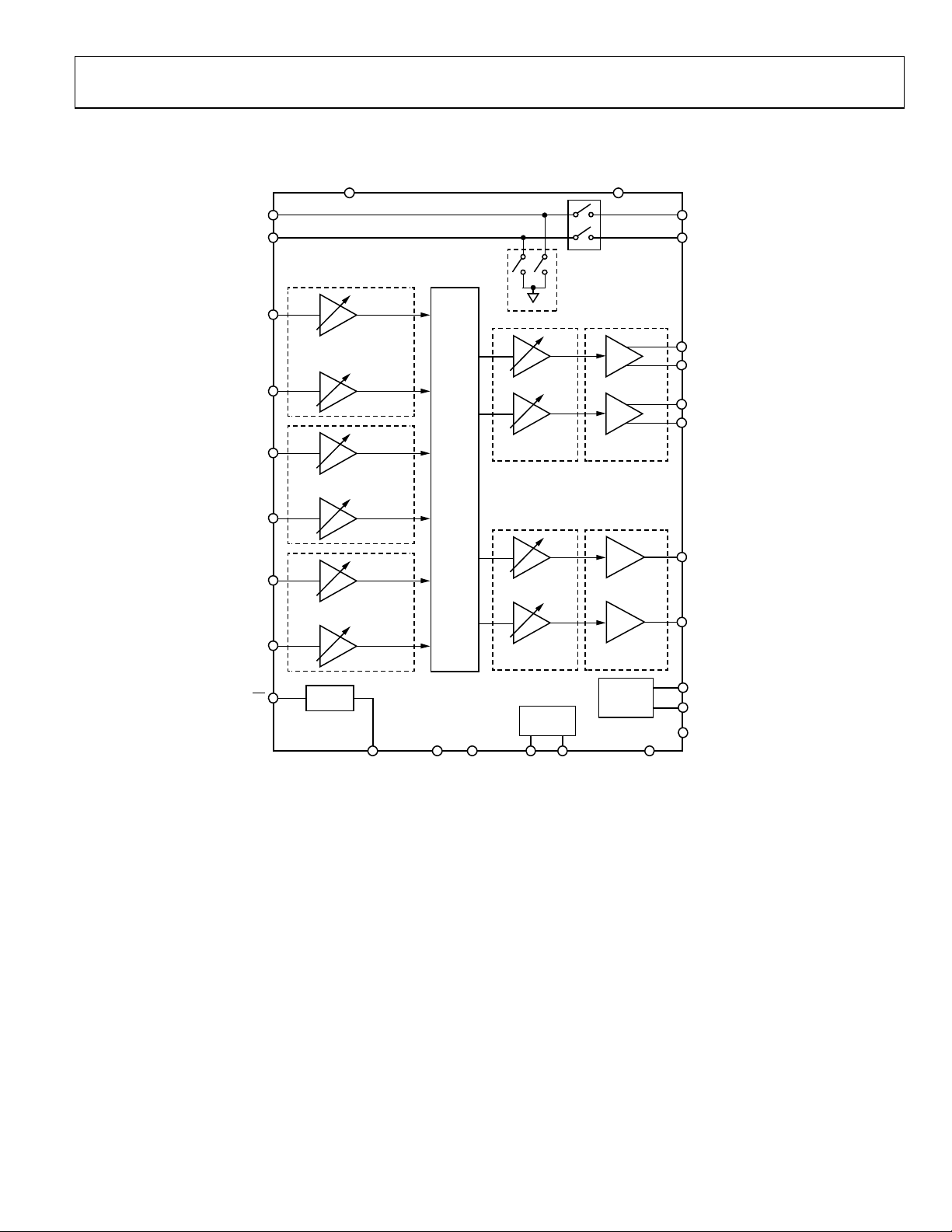
FUNCTIONAL BLOCK DIAGRAM
DD
PVDD
RCV+
RCV–
INA2
INA1
INB2
INB1
INC2
INC1
SD
SSM2804
BOOST = 0dB TO +20dB
PGA = –12dB TO +18dB
BOOST = 0dB TO +20dB
PGA = –12dB TO +18dB
BOOST = 0dB TO +20dB
PGA = –12dB TO +18dB
BIAS
MIX/MUX
+12dB TO –63d B
31 STEPS
0dB TO –75dB
32 STEPS
I2C
CLASS-D
CLASS-G
CLASS-G
SUPPLY
EP+
EP–
LSPK+
LSPK–
RSPK+
RSPK–
HPL
HPR
CF1
CF2
CPVDD
BIAS AGND
PGND SCL SDA CPVSS
09960-001
Figure 1.
Rev. 0 | Page 3 of 36
SSM2804
SPECIFICATIONS
TA = 25°C, AVDD = 3.3 V, PVDD = 3.6 V, gain = 0 dB, unless otherwise noted.
Table 1.
Parameter Min Typ Max Unit Test Conditions/Comments
POWER SUPPLY
Analog Voltage Supply (AVDD) 2.5 3.3 3.6 V
Speaker Voltage Supply (PVDD) 2.7 3.6 5.5 V
Total Quiescent Current (IDD) 3.5 mA HP mode only
6.0 mA Stereo Class-D mode only
9.8 mA HP and Class-D modes
400 µA Receiver path mode
Power-Down Current (ISD) 1 µA
INPUT CHARACTERISTICS
Turn-On Time 10 ms
PGA Mode Operation
Input Impedance 38 54 kΩ Minimum gain setting
4.5 6.5 kΩ Maximum gain setting
Gain Range −12 +18 dB INAx, INBx, INCx inputs, 31 steps
Boost Mode Operation
Input Impedance 20 kΩ
Gain Range 0 20 dB INAx, INBx, INCx inputs, 3 steps
CLASS-D AMPLIFIER
Output Offset Voltage (VOS) 2.3 mV Output muted
12 mV Output unmuted
Output Power (P
) f = 1 kHz, mono operation
OUT
310 mW PVDD = 2.7 V, RL = 8 Ω + 33 µH, THD + N = 1%
700 mW PVDD = 3.6 V, RL = 8 Ω + 33 µH, THD + N = 1%
1.0 W PVDD = 4.2 V, RL = 8 Ω + 33 µH, THD + N = 1%
1.4 W PVDD = 5.0 V, RL = 8 Ω + 33 µH, THD + N = 1%
700 mW PVDD = 2.7 V, RL = 4 Ω + 15 µH, THD + N = 1%
1.5 W PVDD = 3.6 V, RL = 4 Ω + 15 µH, THD + N = 1%
2.0 W PVDD = 4.2 V, RL = 4 Ω + 15 µH, THD + N = 1%
2.9 W PVDD = 5.0 V, RL = 4 Ω + 15 µH, THD + N = 1%
400 mW PVDD = 2.7 V, RL = 8 Ω + 33 µH, THD + N = 10%
860 mW PVDD = 3.6 V, RL = 8 Ω + 33 µH, THD + N = 10%
1.2 W PVDD = 4.2 V, RL = 8 Ω + 33 µH, THD + N = 10%
1.7 W PVDD = 5.0 V, RL = 8 Ω + 33 µH, THD + N = 10%
900 mW PVDD = 2.7 V, RL = 4 Ω + 15 µH, THD + N = 10%
1.8 W PVDD = 3.6 V, RL = 4 Ω + 15 µH, THD + N = 10%
2.5 W PVDD = 4.2 V, RL = 4 Ω + 15 µH, THD + N = 10%
3.6 W PVDD = 5.0 V, RL = 4 Ω + 15 µH, THD + N = 10%
Total Harmonic Distortion Plus Noise
0.01 % R
(THD + N)
Output Noise (Vn) 40 µV 20 Hz to 20 kHz, A-weighted
Signal-to-Noise Ratio (SNR) 94 dB 2.0 V rms output, A-weighted, PVDD = 5 V
Power Supply Rejection Ratio (PSRR) 80 dB 217 Hz, 200 mV p-p ripple
80 dB 1 kHz, 200 mV p-p ripple
Common-Mode Rejection Ratio (CMRR) 55 dB Differential input mode, 1 kHz, 10 mV rms
Efficiency 89 % P
Minimum Load Resistance (R
) 4 Ω
LOAD
Average Switching Frequency (fSW) 400 kHz
Volume Control Gain Range −63 +12 dB
pin low
SD
rising edge from AGND to AVDD
SD
= 8 Ω + 33 µH, P
L
= 700 mW
OUT
= 250 mW
OUT
Rev. 0 | Page 4 of 36
SSM2804
Parameter Min Typ Max Unit Test Conditions/Comments
HEADPHONE OUTPUT
Output Offset Voltage (VOS) 2 mV Headphone only
8 mV INAx, INBx, INCx inputs
Output Power (P
40 mW
Total Harmonic Distortion Plus Noise
(THD + N)
0.02 % RL = 16 Ω, P
Output Noise (Vn) 16 µV 20 Hz to 20 kHz, A-weighted
Signal-to-Noise Ratio (SNR) 96 dB 800 mV rms output, A-weighted
Power Supply Rejection Ratio (PSRR) 95 dB 217 Hz, 200 mV p-p ripple
Crosstalk 90 dB 1 kHz, P
Minimum Load Resistance (R
Maximum Capacitive Load (C
Gain Range −75 0 dB
ESD Protection ±8 kV
RECEIVER PATH (BYPASS SWITCH)
Path Impedance (RON), Receiver Inputs
to Speaker Outputs
Signal Path THD + N 0.1 %
Output Noise 10 µV 20 Hz to 20 kHz, A-weighted
Off Channel Isolation 90 dB 217 Hz, 200 mV p-p ripple
Input Common Mode PVDD/2 V
) 20 mW RL = 32 Ω, THD + N = 1%
OUT
= 16 Ω, THD + N = 1%, 1 µF charge pump
R
L
capacitor
0.012 % R
= 32 Ω, P
L
= 15 mW
OUT
= 10 mW
OUT
85 dB 1 kHz, 200 mV p-p ripple
= 12 mW
OUT
) 16 Ω
LOAD
) 500 pF
LOAD
1.5 Ω RCV+ to EP+ and RCV− to EP−
= 70 mW, RL = 32 Ω or P
P
OUT
= 8 Ω
R
L
= 17.5 mW,
OUT
Table 2. Digital Logic Levels (CMOS Levels)
Parameter Min Typ Max Unit
Input Low Level (VIL) 0.35 V
Input High Level (VIH) 1.35 V
Output Low Level (VOL) 0.1 × AVDD V
Output High Level (VOH) 0.9 × AVDD V
Rev. 0 | Page 5 of 36
SSM2804
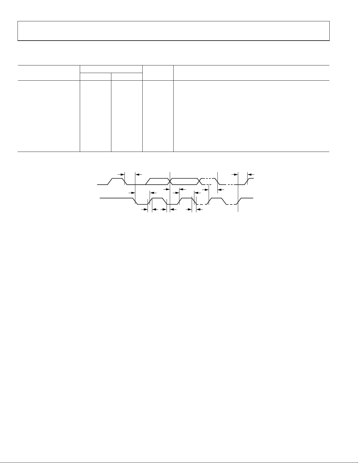
I2C TIMING CHARACTERISTICS
Table 3.
Limit
Parameter
t
600 ns Start condition setup time
SCS
t
600 ns Start condition hold time
SCH
t
MIN
MAX
tPH 600 ns SCL pulse width high
tPL 1.3 s SCL pulse width low
f
0 526 kHz SCL frequency
SCL
tDS 100 ns Data setup time
tDH 900 ns Data hold time
tRT 300 ns SDA and SCL rise time
tFT 300 ns SDA and SCL fall time
t
600 ns Stop condition setup time
HCS
Timing Diagram
SDA
SCL
Unit Description t
t
SCH
t
DS
t
PL
t
RT
Figure 2. I
t
t
DH
2
C Timing
PH
t
t
HCS
t
SCS
FT
09960-002
Rev. 0 | Page 6 of 36
SSM2804
ABSOLUTE MAXIMUM RATINGS
TA = 25°C, unless otherwise noted.
Table 4.
Parameter Rating
Analog Supply Voltage (AVDD) −0.3 V to +3.6 V
Speaker Supply Voltage (PVDD) −0.3 V to +3.6 V
Input Voltage VDD
SD, SCL, SDA, RCV+, RCV−
INA1, INA2, INB1, INB2, INC1, INC2 −0.3 V to AVDD + 0.3 V
ESD (HBM) on Headphone Output 8 kV
Storage Temperature Range −65°C to +150°C
Operating Temperature Range −40°C to +85°C
Junction Temperature Range −65°C to +165°C
Lead Temperature (Soldering, 60 sec) 300°C
Stresses above those listed under Absolute Maximum Ratings
may cause permanent damage to the device. This is a stress
rating only; functional operation of the device at these or any
other conditions above those indicated in the operational
section of this specification is not implied. Exposure to absolute
maximum rating conditions for extended periods may affect
device reliability.
−0.3 V to +6.0 V
THERMAL RESISTANCE
θJA is specified for the worst-case conditions, that is, a device
soldered in a circuit board for surface-mount packages.
Table 5. Thermal Resistance
Package Type PCB θJA θJB Unit
30-Ball, 2.5 mm × 3.0 mm WLCSP 1S0P 162 39 °C/W
2S0P 76 21 °C/W
ESD CAUTION
Rev. 0 | Page 7 of 36
SSM2804
PIN CONFIGURATION AND FUNCTION DESCRIPTIONS
BALL A1
CORNER
1
A
LSPK+
B
LSPK– PGND RSPK– EP– RCV– INA2
234
RSPK+ EP+ RCV+ INA1
PVDD
56
C
D
E
CPVSS SCL SDA INB2 INB1
CF2
AGND CPVDD HPR SD INC2 INC1
CF1 AVDD HPL AGND AVDD BIAS
TOP VIEW
(BALL SIDE DO WN)
Not to Scal e
09960-003
Figure 3. Pin Configuration
Table 6. Pin Function Descriptions
Pin No. Mnemonic Description
A1 LSPK+ Class-D Loudspeaker Output Left +
B1 LSPK− Class-D Loudspeaker Output Left −
C1 CF2 Charge Pump Flyback Capacitor, Terminal 2
D1 AGND Analog Ground
E1 CF1 Charge Pump Flyback Capacitor, Terminal 1
A2 PVDD Speaker Power Supply
B2 PGND Speaker Ground
C2 CPVSS Charge Pump Negative Supply for Class-G
D2 CPVDD Charge Pump Positive Supply for Class-G
E2 AVDD Analog Power Supply
A3 RSPK+ Class-D Loudspeaker Output Right +
B3 RSPK− Class-D Loudspeaker Output Right −
C3 SCL 2-Wire I2C Control Interface Clock Input
D3 HPR Class-G Headphone Output, Right Channel
E3 HPL Class-G Headphone Output, Left Channel
A4 EP+ Integrated Switch Output +
B4 EP− Integrated Switch Output −
C4 SDA 2-Wire I2C Control Interface Data Input/Output
D4
SD
Shutdown Control, Active Low (Optional Limiter Threshold Voltage)
E4 AGND Analog Ground
A5 RCV+ Baseband Receiver (Voice) Input +
B5 RCV− Baseband Receiver (Voice) Input −
C5 INB2 Configurable Input B2 (Single-Ended Input B− or Stereo Input B, Left Channel)
D5 INC2 Configurable Input C2 (Single-Ended Input C− or Stereo Input C, Left Channel)
E5 AVDD Analog Power Supply
A6 INA1 Configurable Input A1 (Single-Ended Input A+ or Stereo Input A, Right Channel)
B6 INA2 Configurable Input A2 (Single-Ended Input A− or Stereo Input A, Left Channel)
C6 INB1 Configurable Input B1 (Single-Ended Input B+ or Stereo Input B, Right Channel)
D6 INC1 Configurable Input C1 (Single-Ended Input C+ or Stereo Input C, Right Channel)
E6 BIAS Device Bias Pin
Rev. 0 | Page 8 of 36
SSM2804
TYPICAL PERFORMANCE CHARACTERISTICS
100
RL = 8Ω + 33µH
10
PVDD = 3.6V
1
100
10
1
RL = 4Ω + 15µH
PVDD = 3.6V
PVDD = 2.7V
0.1
THD + N (%)
0.01
0.001
0.0001 10
0.001 0.01 0.1 1
PVDD = 2.7V
PVDD = 4.2V
PVDD = 5V
OUTPUT POWER (W)
Figure 4. THD + N vs. Output Power into 8 Ω, Class-D Amplifier,
Mono Operation
100
RL = 8Ω + 33µH
10
PVDD = 3.6V
1
0.1
THD + N (%)
0.01
0.001
0.0001 10
0.001 0.01 0.1 1
PVDD = 2.7V
PVDD = 4.2V
PVDD = 5V
OUTPUT POWER (W)
Figure 5. THD + N vs. Output Power into 8 Ω, Class-D Amplifier,
Stereo Operation
0.1
THD + N (%)
0.01
0.001
0.0001 10
09960-004
0.001 0.01 0.1 1
PVDD = 4.2V
OUTPUT POWER (W)
PVDD = 5V
09960-005
Figure 7. THD + N vs. Output Power into 4 Ω, Class-D Amplifier,
Mono Operation
100
RL = 4Ω + 15µH
10
PVDD = 3.6V
1
0.1
THD + N (%)
0.01
0.001
0.0001 10
09960-006
0.001 0.01 0.1 1
PVDD = 2.7V
OUTPUT POWER (W)
PVDD = 4.2V
PVDD = 5V
09960-007
Figure 8. THD + N vs. Output Power into 4 Ω, Class-D Amplifier,
Stereo Operation
100
PVDD = 2.7V
R
= 8Ω + 33µH
L
10
1
0.1
THD + N (%)
0.01
0.001
10 100k
300mW
125mW
62.5mW
100 1k 10k
FREQUENCY (Hz)
Figure 6. THD + N vs. Frequency, Class-D Amplifier, Mono Operation,
= 8 Ω, PVDD = 2.7 V
R
L
09960-008
Rev. 0 | Page 9 of 36
100
PVDD = 2.7V
R
= 4Ω + 15µH
L
10
1
0.1
THD + N (%)
0.01
0.001
10 100k
500mW
62.5mW
100 1k 10k
250mW
125mW
FREQUENCY (Hz)
Figure 9. THD + N vs. Frequency, Class-D Amplifier, Mono Operation,
RL = 4 Ω, PVDD = 2.7 V
09960-009
SSM2804
100
10
PVDD = 3.6V
R
= 8Ω + 33µH
L
100
10
PVDD = 3.6V
R
=4Ω + 15µH
L
1
0.1
THD + N (%)
0.01
0.001
10 100k
600mW
500mW
250mW
100 1k 10k
FREQUENCY (Hz)
125mW
Figure 10. THD + N vs. Frequency, Class-D Amplifier, Mono Operation,
= 8 Ω, PVDD = 3.6 V
R
L
100
PVDD = 4.2V
R
=8Ω + 33µH
L
10
1
0.1
THD + N (%)
0.01
900mW
250mW
125mW
1
0.1
THD + N (%)
0.01
0.001
10 100k
09960-010
1.1W
125mW
100 1k 10k
250mW
500mW
FREQUENCY (Hz)
09960-011
Figure 13. THD + N vs. Frequency, Class-D Amplifier, Mono Operation,
= 4 Ω, PVDD = 3.6 V
R
L
100
PVDD = 4.2V
R
=4Ω + 15µH
L
10
250mW
1.5W
1W
1
0.1
THD + N (%)
0.01
0.001
10 100k
100 1k 10k
FREQUENCY (Hz)
500mW
Figure 11. THD + N vs. Frequency, Class-D Amplifier, Mono Operation,
= 8 Ω, PVDD = 4.2 V
R
L
100
PVDD = 5V
R
= 8Ω + 33µH
L
10
1
0.1
THD + N (%)
0.01
0.001
10 100k
1.2W
250mW
100 1k 10k
FREQUENCY (Hz)
1W
500mW
Figure 12. THD + N vs. Frequency, Class-D Amplifier, Mono Operation,
= 8 Ω, PVDD = 5.0 V
R
L
0.001
10 100k
09960-012
100 1k 10k
FREQUENCY (Hz)
500mW
09960-013
Figure 14. THD + N vs. Frequency, Class-D Amplifier, Mono Operation,
= 4 Ω, PVDD = 4.2 V
R
L
100
PVDD = 5V
R
= 4Ω + 15µH
L
10
1
0.1
THD + N (%)
0.01
0.001
10 100k
09960-014
2.2W
250mW
100 1k 10k
FREQUENCY (Hz)
1.5W
500mW
09960-015
Figure 15. THD + N vs. Frequency, Class-D Amplifier, Mono Operation,
= 4 Ω, PVDD = 5.0 V
R
L
Rev. 0 | Page 10 of 36
SSM2804
2.0
f = 1kHz
1.8
R
= 8Ω + 33µH
1.6
1.4
1.2
1.0
0.8
0.6
OUTPUT POWER (W)
0.4
0.2
L
THD + N = 1%
THD + N = 10%
0
2.5 3.0 3.5 4.0 4.5 5.0
SUPPLY VOLTAGE (V)
THD + N = 0.1%
Figure 16. Output Power vs. Supply Voltage, Class-D Amplifier, RL = 8 Ω
09960-016
3.5
f = 1kHz
3.0
R
= 4Ω + 15µH
L
2.5
2.0
1.5
OUTPUT POWER (W)
1.0
0.5
THD + N = 10%
0
2.5 3.0 3.5 4.0 4.5 5.0
THD + N = 1%
THD + N = 0.1%
SUPPLY VOLTAGE (V)
Figure 19. Output Power vs. Supply Voltage, Class-D Amplifier, RL = 4 Ω
09960-017
400
RL = 8Ω + 33µH
350
300
250
200
150
SUPPLY CURRENT (mA)
100
PVDD = 2.7V
50
0
0.2 0.4 0.6 0.8 1.0 1.2 1.4 1.6 1.8
02
PVDD = 3.6V
OUTPUT PO WER (W)
PVDD = 4.2V
PVDD = 5V
.0
09960-018
Figure 17. Supply Current vs. Output Power into 8 Ω, Class-D Amplifier
100
PVDD = 2.7V
90
80
70
60
PVDD = 3.6V
50
40
EFFICIENCY (%)
30
20
10
0
0 0.2 0.4 0. 6 0.8 1.0 1.2 1.4 1.6 1.8
PVDD = 5V
PVDD = 4.2V
OUTPUT PO WER (W)
RL = 8Ω + 33µH
09960-020
Figure 18. Efficiency vs. Output Power into 8 Ω, Class-D Amplifier
800
RL = 4Ω + 15µH
700
600
500
400
300
PVDD = 2.7V
SUPPLY CURRENT (mA)
200
100
0
03
Figure 20. Supply Current vs. Output Power into 4 Ω, Class-D Amplifier
100
90
80
70
60
50
40
EFFICIENCY (%)
30
20
10
0
0 0.2 0. 4 0. 6 0.8 1.0 1. 2 1. 4 1.6 1.8 2. 0 2. 2 2.4 2.6 2.8 3.0
Figure 21. Efficiency vs. Output Power into 4 Ω, Class-D Amplifier
PVDD = 4.2V
PVDD = 3.6V
0.5 1.0 1.5 2.0 2.5 3.0
OUTPUT PO WER (W)
PVDD = 2.7V
PVDD = 3.6V
PVDD = 4.2V
PVDD = 5V
OUTPUT PO WER (W)
PVDD = 5V
RL = 4Ω + 15µH
.5
09960-019
09960-021
Rev. 0 | Page 11 of 36

SSM2804
–
–
100
RL = 16Ω
100
RL = 32Ω
10
1
0.1
THD + N (%)
0.01
0.001
0.0001 10
0.001 0.01 0.1 1
OUTPUT POWER (W)
Figure 22. THD + N vs. Output Power into 16 Ω, Headphone Amplifier,
Stereo Operation
100
PVDD = 2.7V
R
= 16Ω
L
10
1
0.1
THD + N (%)
10mW
10
1
0.1
THD + N (%)
0.01
0.001
0.0001 10
09960-023
0.001 0.01 0.1 1
OUTPUT PO WER (W)
09960-024
Figure 25. THD + N vs. Output Power into 32 Ω, Headphone Amplifier,
Stereo Operation
100
PVDD = 2.7V
R
= 32Ω
L
10
1
0.1
THD + N (%)
5mW
0.01
0.001
10 100k
100 1k 10k
20mW
FREQUENCY (Hz)
Figure 23. THD + N vs. Frequency, Headphone Amplifier,
= 16 Ω, PVDD = 2.7 V
R
L
20
–30
–40
–50
–60
–70
PSRR (dB)
–80
–90
–100
–110
–120
10 100k
100 1k 10k
FREQUENCY (Hz)
Figure 24. Power Supply Rejection Ratio (PSRR) vs. Frequency,
Class-D Amplifier
0.01
0.001
10 100k
09960-025
100 1k 10k
FREQUENCY (Hz)
10mW
09960-026
Figure 26. THD + N vs. Frequency, Headphone Amplifier,
RL = 32 Ω, PVDD = 2.7 V
20
–30
–40
–50
–60
–70
PSRR (dB)
–80
–90
–100
–110
–120
10 100k
09960-022
100 1k 10k
FREQUENCY (Hz)
09960-027
Figure 27. Power Supply Rejection Ratio (PSRR) vs. Frequency,
Headphone Amplifier
Rev. 0 | Page 12 of 36

SSM2804
THEORY OF OPERATION
The SSM2804 audio subsystem features a filterless modulation
scheme that greatly reduces the external component count, conserving board space and, thus, reducing system cost. The SSM2804
does not require an output filter but, instead, relies on the inherent
inductance of the speaker coil and the natural filtering of the
speaker and human ear to fully recover the audio component
of the square wave output.
Most Class-D amplifiers use some variation of pulse-width
modulation (PWM), but the SSM2804 uses Σ-Δ modulation to
determine the switching pattern of the output devices, resulting
in a number of important benefits.
• Σ-Δ modulators do not produce a sharp peak with many
harmonics in the AM frequency band, as pulse-width
modulators often do.
• Σ-Δ modulation provides the benefits of reducing the
amplitude of spectral components at high frequencies,
that is, reducing EMI emissions that might otherwise
be radiated by speakers and long cable traces.
• The SSM2804 does not require external EMI filtering for
twisted speaker cable lengths shorter than 10 cm. If longer
speaker cables are used, the SSM2804 has emission limiting
circuitry that allows significantly longer speaker cable.
• Due to the inherent spread-spectrum nature of Σ-Δ modu-
lation, the need for modulator synchronization is eliminated
for designs that incorporate multiple SSM2804 amplifiers.
Using the I
2
C control interface, the gain of the SSM2804 can
be selected from a range of +12 dB to −63 dB in 32 steps. Other
features accessed from the I
2
C interface include the following:
• Independent left/right channel shutdown
• Variable ultralow EMI emission limiting circuitry
• Automatic level control (ALC) for high quality speaker
protection
• Stereo-to-mono mixing operation
The SSM2804 also offers protection circuits for overcurrent and
overtemperature protection.
POP-AND-CLICK SUPPRESSION
Voltage transients at the output of audio amplifiers can occur
when shutdown is activated or deactivated. Voltage transients
as low as 10 mV can be heard as an audio pop in the speaker.
Clicks and pops can also be classified as undesirable audible
transients generated by the amplifier system and, therefore, as
not coming from the system input signal. Such transients may
be generated when the amplifier system changes its operating
mode. For example, the following may be sources of audible
transients: system power-up and power-down, mute and
unmute, input source change, and sample rate change.
The SSM2804 has a pop-and-click suppression architecture that
reduces these output transients, resulting in noiseless activation
and deactivation.
OUTPUT MODULATION DESCRIPTION
The SSM2804 uses three-level, Σ-Δ output modulation. Each
output can swing from GND to V
no input signal is present, the output differential voltage is 0 V
because there is no need to generate a pulse. In a real-world
situation, noise sources are always present.
Due to the constant presence of noise, a differential pulse is
generated, when required, in response to this stimulus. A small
amount of current flows into the inductive load when the differential pulse is generated.
Most of the time, however, the output differential voltage is 0 V,
due to the Analog Devices, Inc., three-level, Σ-Δ output modulation. This feature ensures that the current flowing through the
inductive load is small.
When the user wants to send an input signal, an output pulse
(OUT+ and OUT−) is generated to follow the input voltage.
The differential pulse density (V
input signal level. Figure 28 depicts three-level, Σ-Δ output
modulation with and without input stimulus.
OUTPUT = 0V
OUT+
OUT–
V
OUT
OUTPUT > 0V
OUT+
OUT–
V
OUT
OUTPUT < 0V
OUT+
OUT–
V
OUT
Figure 28. Three-Level, Σ-Δ Output Modulation
With and Without Input Stimulus
and vice versa. Ideally, when
DD
) is increased by raising the
OUT
+5V
0V
+5V
0V
+5V
0V
–5V
+5V
0V
+5V
0V
+5V
0V
+5V
0V
+5V
0V
0V
–5V
09960-104
Rev. 0 | Page 13 of 36

SSM2804
HARDWARE-BASED HEADPHONE LIMITER
To provide fail-safe headphone level limiting independent of
the register values sent to the amplifier over the I
SSM2804 incorporates an optional hardware-based headphone
limiter feature. The user controls the limiter level by supplying
a voltage at the
SD
pin (see ). The hardware limiter is
Tabl e 7
activated by setting the LIM_MODE bit to 0 in the additional
control register (Bit D3 of Register 0x0E). After the desired
limiter value is set, the user can lock the limiter setting by
setting the LIMLOCK bit (Bit D7 of Register 0x0E).
Table 7. Hardware Limiter Options
Limiter
Level
Power into
32 Ω (mW)
Power into
16 Ω (mW)
Shutdown N/A N/A <0.87 V
±0.40 V 2.5 5 0.87 V < VSD < 1.08 V
±8 V 10 20 1.08 V < VSD < 1.29 V
±1.13 V 20 40 VSD > 1.29 V
Note that after the hardware limiter lock bit is set, the locked
levels cannot be reset until the SSM2804 is powered down, the
SD
pin is strobed low, or all eight bits of the software reset
register (Register 0x10) are set to 0.
In addition to the hardware-based limiter, several other limiter
levels can be selected using the I
2
C-based limiter function (set
the HPLIM bits of Register 0x0E; see Tabl e 44 ). The effect of
the limiter function on the headphone output is shown in
Figure 29.
CH1 500mV
B
W
Figure 29. Limited Headphone Signal
M20.0ms A CH1 110mV
2
C bus, the
Pin Voltage
SD
09960-028
ACTIVATING OR DEACTIVATING THE EMISSION LIMITING CIRCUITRY
To activate or deactivate the emission limiting circuitry, change
the value of the EDGE bits in the additional control register
(Bits[D1:D0] of Register 0x0E). Four levels of emission control
are available, allowing the user to determine the best trade-off
between efficiency and EMI reduction.
In the default (fastest edge) mode, the user can pass FCC
Class-B emission testing with 10 cm twisted pair speaker wire
for loudspeaker connection. If longer speaker wire is desired,
change the EDGE setting to a slower edge rate mode.
Rev. 0 | Page 14 of 36
The trade-off is slightly lower efficiency and noise performance.
The penalty for using the emission control circuitry is far less
than the decreased performance observed when using a ferrite
bead based EMI filter for emission limiting purposes.
AUTOMATIC LEVEL CONTROL (ALC)
Automatic level control (ALC) is a function that automatically
adjusts amplifier gain to generate the desired output amplitude
with reference to a particular input stimulus. The primary use for
the ALC is to protect an audio power amplifier or speaker load
from the damaging effects of clipping or current overloading.
This is accomplished by limiting the output amplitude of the
amplifier upon reaching a preset threshold voltage. Another
benefit of the ALC is that it makes sound sources with a wide
dynamic range more intelligible by boosting low level signals
and limiting very high level signals.
Before activating the ALC by setting the ALCEN bit (Bit D7
of Register 0x0B), the user has full control of the left and right
channel PGA gain. After the ALC is activated (ALCEN = 1),
the user has no control over the gain settings; the left channel
PGA gain is locked into the device and controls the gain for both
the left and right channels. To change the gain, the user must
reset the ALCEN bit to 0 and then load the new gain settings.
Figure 30 shows the response of the SSM2804 to a linearly
increasing input signal. When the output reaches the current
threshold value, the amplifier gain decreases by 0.5 dB so that
the output voltage remains under the threshold. As more attenuation is added to the system, the threshold increases according
to a profile determined by the compressor setting bits in the
ALC Control 2 register (Bits[D6:D5] of Register 0x0B), causing
a rounded “knee” as the output voltage approaches the output
limiter level. The effect of this compression curve is shown in
Figure 30.
5.6
5.2
4.8
4.4
4.0
3.6
3.2
2.8
2.4
2.0
1.6
OUTPUT VOLTAGE LEVEL (V)
1.2
0.8
0.4
0
0 20 40 60 80 100 120 140 160 180 200
Figure 30. Output Response to Linearly Increasing Input Ramp Signal
TIME (ms)
When the input level is small and the output voltage is smaller
than the ALC threshold value, the gain of the amplifier stays at
the preset gain setting. When the input exceeds the ALC threshold value, the ALC gradually reduces the gain from the preset
gain setting down to 1 dB.
INPUT
GAIN = 6dB
GAIN = 12dB
GAIN = 18dB
GAIN = 24dB
09960-034

SSM2804
ALC Compression and Limiter Modes
The ALC implemented on the SSM2804 has two operation
modes: compression mode and limiter mode. When the ALC
is triggered for medium-level input signals, the ALC is in compression mode. In this mode, an increase of the output signal is
one-third the increase of the input signal. For example, if the
input signal increases by 3 dB, the ALC reduces the amplifier
gain by 2 dB and, thus, the output signal increases by only 1 dB.
As the input signal becomes very large, the ALC transitions to
limiter mode. In this mode, the output stays at a given threshold
level, V
, even if the input signal grows larger. As an example of
TH
limiter mode operation, when a large input signal increases by
3 dB, the ALC reduces the amplifier gain by 3 dB and, thus, the
output increases by 0 dB. When the amplifier gain is reduced to
1 dB, the ALC cannot reduce the gain further, and the output
increases again. This is because the total range of the ALC operation has bottomed out due to extreme input voltage at high gain. To
avoid potential speaker damage, the maximum input amplitude
should not be large enough to exceed the maximum attenuation
(to a level of 1 dB) of the limiter mode.
Attack Time, Hold Time, and Release Time
When the amplifier input signal exceeds a preset threshold,
the ALC reduces amplifier gain rapidly until the output voltage
settles to a target level. This target level is maintained for a certain
period. If the input voltage does not exceed the threshold again,
the ALC increases the gain gradually.
The attack time is the time taken to reduce the gain from maximum to minimum. The hold time is the time that the reduced
gain is maintained. The release time is the time taken to increase
the gain from minimum to maximum. These times are shown
in Tab l e 8. The attack time and the release time can be set using
the ALC 1 control register (Address 0x0A).
Table 8. ALC Attack, Hold, and Release Times
Time1 Duration
Attack Time 32 s to 4 ms (per 0.5 dB step)
Hold Time 90 ms to 120 ms
Release Time 4 ms to 512 ms (per 0.5 dB step)
1
The attack time and release time can be adjusted using the I2C interface.
The hold time cannot be adjusted.
Soft-Knee Compression
Often performed using sophisticated DSP algorithms, soft-knee
compression provides maximum sound quality with effective
speaker protection. Instead of using a fixed compression setting
prior to limiting, the SSM2804 allows for a much more subtle
transition into limiting mode, preserving the original sound
quality of the source audio. Figure 31 to Figure 33 show the
various soft-knee compression settings that can be selected
using the COMP bit settings (Bits[D6:D5] of Register 0x0B).
2.5
2.0
1.5
1.0
OUTPUT VOLTAGE (V)
0.5
0
0 0.05 0.10 0.15 0.20 0.30 0.35 0.40 0.450.25 0. 50
INPUT VOLTAGE (V)
00 (COMPRESSION MODE 1)
01 (COMPRESSION MODE 2)
10 (COMPRESSION MODE 3)
11 (LIMITER MODE)
2.7V × 0.78 = 2.106V
Figure 31. Adjustable Compression Settings, PVDD = 2.7 V,
ALC Threshold Level = 78%
3.5
3.0
2.5
2.0
1.5
OUTPUT VOLTAGE (V)
1.0
0.5
0
0 0.1 0.2 0.3 0.4 0.6 0.7 0.8 0.90.5 1.0
INPUT VOLTAGE (V)
00 (COMPRESSION MODE 1)
01 (COMPRESSION MODE 2)
10 (COMPRESSION MODE 3)
11 (LIMITER MODE)
3.6V × 0.78 = 2.808V
Figure 32. Adjustable Compression Settings, PVDD = 3.6 V,
ALC Threshold Level = 78%
4.5
4.0
3.5
3.0
2.5
2.0
1.5
OUTPUT VOLTAGE (V)
1.0
0.5
0
0 0.2 0.4 0.6 0.8 1.2 1.4 1.6 1.81.0 2.0
INPUT VOLTAGE (V)
00 (COMPRESSION MODE 1)
01 (COMPRESSION MODE 2)
10 (COMPRESSION MODE 3)
11 (LIMITER MODE)
5.0V × 0.78 = 3.9V
Figure 33. Adjustable Compression Settings, PVDD = 5.0 V,
ALC Threshold Level = 78%
09960-107
9960-118
9960-119
Rev. 0 | Page 15 of 36

SSM2804
A
ALC Soft Transition
The ALC operation of the SSM2804 incorporates techniques to
reduce the audible artifacts associated with gain change transitions. First, the gain is changed in small increments of 0.5 dB.
In addition to this small step size, the rate of gain change is
reduced, proportional to the attack time setting. This feature
drastically reduces and virtually eliminates the presence of zipper
noise and other artifacts associated with gain transitions during
ALC operation. Figure 34 shows the soft transition operation.
L TRANSITION
NORM
0.5dB
SOFT T RANSITION (32µs TO 256µs)
0.5dB
09960-108
Figure 34. Soft Transition
Rev. 0 | Page 16 of 36

SSM2804
TYPICAL APPLICATION CIRCUITS
0.1µF
PVDDAVDD
10µF
EARPIECE
EP+
EP–
CLASS-D
OUTPUT LEFT
LSPK+
LSPK–
RSPK+
RCV IN+
RCV IN–
LSPK IN–
(DIFF IN1–)
LSPK IN+
(DIFF IN1+)
0.1µF
0.1µF
10µF
RCV+
RCV–
INA2
INA1
0.1µF
AVDD
2.5V TO 3. 6V
SSM2804
BOOST = 0 dB TO +20dB
PGA = –12dB TO +18dB
VBATT
2.7V TO 5.5V
RSPK–
OUTPUT RIGHT
HPL
HPR
CF1
CF2
CPVDD
CPVDD
1.2V TO 2.2V
1µF TO 2. 2µF
CLASS-D
HEADPHONE
OUTPUT LEFT
HEADPHONE
OUTPUT RIGHT
1µF
1µF TO 2. 2µF
09960-031
MP3 INL
(DIFF IN2–)
MP3 INR
(DIFF IN2+)
FM INL
(DIFF IN3–)
FM INR
(DIFF IN3+)
SHUTDOWN
0.1µF
0.1µF
0.1µF
0.1µF
INB2
BOOST = 0 dB TO +20dB
PGA = –12dB TO +18dB
INB1
INC2
BOOST = 0 dB TO +20dB
PGA = –12dB TO +18dB
INC1
SD
BIAS
BIAS
AGND
+12dB TO –63d B
31 STEPS
MIX/MUX
0dB TO –75d B
32 STEPS
PGND SCL SDA
I2C
2
I
C DATA
2
I
C CLOCK
CLASS-D
CLASS-G
CLASS-G
SUPPLY
CPVSS
CPVSS
–2.2V TO +1.2V
Figure 35. Application Circuit with External Components
Rev. 0 | Page 17 of 36

SSM2804
BYPASS
CLASS-D
MIX/MUX
CLASS-G
1.2V < CPVDD < +2. 2V/–2.2V < CPVSS < –1.2V (INTERNAL LY GENERATED)
2.7V < PVDD < 5V
2.5V < AVDD < 3.6V
09960-032
Figure 36. Power Supply Domains
Rev. 0 | Page 18 of 36

SSM2804
A
A
I2C SOFTWARE CONTROL INTERFACE
The I2C interface provides access to the user-selectable control
registers and operates with a 2-wire interface.
Each control register consists of 16 bits, MSB first. Bits[B15:B9]
are the register map address, and Bits[B8:B0] are the register data
for the associated register map.
SDA
SCL
S
1TO 7
START ADDR R/W
98
ACK ACKSUBADDRESS ACK STOPDATA
1TO 7
Figure 37. 2-Wire I
WRITE
SEQUENCE
SEQUENCE
S/P = START/STOP BIT.
A0 = I2C R/W BIT.
A(S) = ACKNOWLEDGE BY SLAVE.
(M) = ACKNOWLEDGE BY MASTER.
(M) = ACKNOWLEDGE BY MASTER (INVERSION).
SA1A7 A0 A(S) A(S) A(S)B15 B9 B8
READ
SA1A7 A0 A(S) A(S) SB15 B9 0
... ...
DEVICE
ADDRESS
DEVICE
ADDRESS
0
01
REGISTER
ADDRESS
REGISTER
ADDRESS
Figure 38. I
REGISTER
DATA
2
2
C Generalized Clocking Diagram
C Write and Read Sequences
SDA generates the serial control data-word, and SCL
clocks the serial data. The I
2
C bus address (Bits[A7:A1]) is
0x3B (01110110 for write and 01110111 for read). Bit A0 is
the designated read/write bit.
98
B0B7 P...
DEVICE
ADDRESS
1TO 7
98
P
0P
REGISTER
DATA
(SLAVE DRIVE)
09960-029
0... A1A7 A0 A(S)... B0 B8B7 A(M) A(M)...
......
09960-030
Rev. 0 | Page 19 of 36

SSM2804
REGISTER MAP
The 7-bit I2C address of the SSM2804 is 0x3B (0111011).
Table 9. Register Map
Address Name D7 D6 D5 D4 D3 D2 D1 D0 Default
0x00 Input mode 0 ZCD GAINMOD[2:0] INMOD[2:0] 0x00
0x01 INA volume 0 0 0 INAVOL[4:0] 0x00
0x02 INB volume 0 0 0 INBVOL[4:0] 0x00
0x03 INC volume 0 0 0 INCVOL[4:0] 0x00
0x04
0x05
0x06 LHP volume 0 0 0 LHPVOL[4:0] 0x00
0x07 RHP volume 0 0 0 RHPVOL[4:0] 0x00
0x08 HP input mixer POPTIME[1:0] RHPMOD[2:0] LHPMOD[2:0] 0x00
0x09
0x0A ALC Control 1 0 0 RECTIME[2:0] ATTIME[2:0] 0x2B
0x0B ALC Control 2 ALCEN COMP[1:0] ALCLV_FIX ALCLV[3:0] 0x4B
0x0C ALC Control 3 0 LCDBOOST RCDBOOST SOFTSTART SOFTCLIPEN NGEN NGATE[1:0] 0x00
0x0D
0x0E
0x0F Chip status1 0 0 0 0 OCCD OCHP OW OT 0x00
0x10 Software reset2 SOFTRESET 0x00
1
This byte is read-only.
2
This byte is write-only.
Class-D left
volume
Class-D right
volume
Class-D input
mixer
Power- down
control
Additional
control
0 0 0 LCDVOL[4:0] 0x00
0 0 0 RCDVOL[4:0] 0x00
CDSM[1:0] RCDMOD[2:0] LCDMOD[2:0] 0x00
PASSPDB INCPDB INBPDB INAPDB RCDPDB LCDPDB HPPDB PWDB 0x00
LIMLOCK HPLIM[2:0] LIM_MOD TO EDGE[1:0] 0x00
Rev. 0 | Page 20 of 36

SSM2804
REGISTER MAP DETAILS
INPUT CHANNEL MODE CONTROL, ADDRESS 0x00
Table 10. Input Channel Mode Control Register Bit Map
D7 D6 D5 D4 D3 D2 D1 D0
0 ZCD GAINMOD[2:0] INMOD[2:0]
Table 11. Input Channel Mode Control Register Bit Descriptions
Bit Name Description Settings
ZCD Zero cross-detector enable 0 = disable (default)
1 = enable
GAINMOD[2:0] Input amplifier gain mode xx0 = Input A PGA mode
xx1 = Input A boost mode
x0x = Input B PGA mode
x1x = Input B boost mode
0xx = Input C PGA mode
1xx = Input C boost mode
INMOD[2:0] Input mode control xx0 = Input A stereo mode (INA1, INA2 > INAL, INAR)
xx1 = Input A differential mode (INA1, INA2 > INA+, INA−)
x0x = Input B stereo mode (INB1, INB2 > INBL, INBR)
x1x = Input B differential mode (INB1, INB2 > INB+, INB−)
0xx = Input C stereo mode (INC1, INC2 > INCL, INCR)
1xx = Input C differential mode (INC1, INC2 > INC+, INC−)
See Tab le 12 for complete information about the naming table
Table 12. Input Mode Naming Table
INMOD[2:0] INA1 Pin INA2 Pin INB1 Pin INB2 Pin INC1 Pin INC2 Pin
000 INAL INAR INBL INBR INCL INCR
001 INAL INAR INBL INBR INC+ INC−
010 INAL INAR INB+ INB− INCL INCR
011 INAL INAR INB+ INB− INC+ INC−
100 INA+ INA− INBL INBR INCL INCR
101 INA+ INA− INBL INBR INC+ INC−
110 INA+ INA− INB+ INB− INCL INCR
111 INA+ INA− INB+ INB− INC+ INC−
Rev. 0 | Page 21 of 36

SSM2804
CHANNEL A LINE INPUT VOLUME, ADDRESS 0x01
Table 13. Channel A Line Input Volume Register Bit Map
D7 D6 D5 D4 D3 D2 D1 D0
0 0 0 INAVOL[4:0]
Table 14. Channel A Line Input Volume Register Bit Descriptions
Bit Name Description Settings
INAVOL[4:0] Analog Channel A input volume control See Table 1 5
Table 15. Descriptions of Channel A Volume Register Bits
INAVOL[4:0] PGA Mode (dB) Boost Mode (dB)
00000 Mute Mute
00001 −12 0
00010 −11 0
00011 −10 0
00100 −9 0
00101 −8 0
00110 −7 0
00111 −6 0
01000 −5 0
01001 −4 0
01010 −3 0
01011 −2 0
01100 −1 0
01101 0 0
01110 1 9
01111 2 9
10000 3 9
10001 4 9
10010 5 9
10011 6 9
10100 7 20
10101 8 20
10110 9 20
10111 10 20
11000 11 20
11001 12 20
11010 13 20
11011 14 20
11100 15 20
11101 16 20
11110 17 20
11111 18 20
Rev. 0 | Page 22 of 36

SSM2804
CHANNEL B LINE INPUT VOLUME, ADDRESS 0x02
Table 16. Channel B Line Input Volume Register Bit Map
D7 D6 D5 D4 D3 D2 D1 D0
0 0 0 INBVOL[4:0]
Table 17. Channel B Line Input Volume Register Bit Descriptions
Bit Name Description Settings
INBVOL[4:0] Analog Channel B input volume control See Table 18
Table 18. Descriptions of Channel B Input Volume Register Bits
INBVOL[4:0] PGA Mode (dB) Boost Mode (dB)
00000 Mute Mute
00001 −12 0
00010 −11 0
00011 −10 0
00100 −9 0
00101 −8 0
00110 −7 0
00111 −6 0
01000 −5 0
01001 −4 0
01010 −3 0
01011 −2 0
01100 −1 0
01101 0 0
01110 1 9
01111 2 9
10000 3 9
10001 4 9
10010 5 9
10011 6 9
10100 7 20
10101 8 20
10110 9 20
10111 10 20
11000 11 20
11001 12 20
11010 13 20
11011 14 20
11100 15 20
11101 16 20
11110 17 20
11111 18 20
Rev. 0 | Page 23 of 36

SSM2804
CHANNEL C LINE INPUT VOLUME, ADDRESS 0x03
Table 19. Channel C Line Input Volume Register Bit Map
D7 D6 D5 D4 D3 D2 D1 D0
0 0 0 INCVOL[4:0]
Table 20. Channel C Line Input Volume Register Bit Descriptions
Bit Name Description Settings
INCVOL[4:0] Analog Channel C input volume control See Table 21
Table 21. Descriptions of Channel C Input Volume Register Bits
INCVOL[4:0] PGA Mode (dB) Boost Mode (dB)
00000 Mute Mute
00001 −12 0
00010 −11 0
00011 −10 0
00100 −9 0
00101 −8 0
00110 −7 0
00111 −6 0
01000 −5 0
01001 −4 0
01010 −3 0
01011 −2 0
01100 −1 0
01101 0 0
01110 1 9
01111 2 9
10000 3 9
10001 4 9
10010 5 9
10011 6 9
10100 7 20
10101 8 20
10110 9 20
10111 10 20
11000 11 20
11001 12 20
11010 13 20
11011 14 20
11100 15 20
11101 16 20
11110 17 20
11111 18 20
Rev. 0 | Page 24 of 36

SSM2804
CLASS-D LEFT LOUDSPEAKER OUTPUT VOLUME, ADDRESS 0x04
Table 22. Class-D Left Loudspeaker Output Volume Register Bit Map
D7 D6 D5 D4 D3 D2 D1 D0
0 0 0 LCDVOL[4:0]
Table 23. Class-D Left Loudspeaker Output Volume Register Bit Descriptions
Bit Name Description Settings
LCDVOL[4:0] Left channel Class-D volume control 00000 = mute (default)
00001 = −75 dB
00010 = −71 dB
00011 = −67 dB
00100 = −63 dB
00101 = −59 dB
00110 = −55 dB
00111 = −51 dB
01000 = −47 dB
01001 = −44 dB
01010 = −41 dB
01011 = −38 dB
01100 = −35 dB
01101 = −32 dB
01110 = −29 dB
01111 = −26 dB
10000 = −23 dB
10001 = −21 dB
10010 = −19 dB
10011 = −17 dB
10100 = −15 dB
10101 = −13 dB
10110 = −11 dB
10111 = −9 dB
11000 = −7 dB
11001 = −6 dB
11010 = −5 dB
11011 = −4 dB
11100 = −3 dB
11101 = −2 dB
11110 = −1 dB
11111 = 0 dB
Rev. 0 | Page 25 of 36

SSM2804
CLASS-D RIGHT LOUDSPEAKER OUTPUT VOLUME, ADDRESS 0x05
Table 24. Class-D Right Loudspeaker Output Volume Register Bit Map
D7 D6 D5 D4 D3 D2 D1 D0
0 0 0 RCDVOL[4:0]
Table 25. Class-D Right Loudspeaker Output Volume Register Bit Descriptions
Bit Name Description Settings
RCDVOL[4:0] Right channel Class-D volume control 00000 = mute (default)
00001 = −75 dB
00010 = −71 dB
00011 = −67 dB
00100 = −63 dB
00101 = −59 dB
00110 = −55 dB
00111 = −51 dB
01000 = −47 dB
01001 = −44 dB
01010 = −41 dB
01011 = −38 dB
01100 = −35 dB
01101 = −32 dB
01110 = −29 dB
01111 = −26 dB
10000 = −23 dB
10001 = −21 dB
10010 = −19 dB
10011 = −17 dB
10100 = −15 dB
10101 = −13 dB
10110 = −11 dB
10111 = −9 dB
11000 = −7 dB
11001 = −6 dB
11010 = −5 dB
11011 = −4 dB
11100 = −3 dB
11101 = −2 dB
11110 = −1 dB
11111 = 0 dB
Rev. 0 | Page 26 of 36

SSM2804
LEFT HEADPHONE OUTPUT VOLUME, ADDRESS 0x06
Table 26. Left Headphone Output Volume Register Bit Map
D7 D6 D5 D4 D3 D2 D1 D0
0 0 0 LHPVOL[4:0]
Table 27. Left Headphone Output Volume Register Bit Descriptions
Bit Name Description Settings
LHPVOL[4:0] Left headphone output volume control 00000 = mute (default)
00001 = −75 dB
00010 = −71 dB
00011 = −67 dB
00100 = −63 dB
00101 = −59 dB
00110 = −55 dB
00111 = −51 dB
01000 = −47 dB
01001 = −44 dB
01010 = −41 dB
01011 = −38 dB
01100 = −35 dB
01101 = −32 dB
01110 = −29 dB
01111 = −26 dB
10000 = −23 dB
10001 = −21 dB
10010 = −19 dB
10011 = −17 dB
10100 = −15 dB
10101 = −13 dB
10110 = −11 dB
10111 = −9 dB
11000 = −7 dB
11001 = −6 dB
11010 = −5 dB
11011 = −4 dB
11100 = −3 dB
11101 = −2 dB
11110 = −1 dB
11111 = 0 dB
Rev. 0 | Page 27 of 36

SSM2804
RIGHT HEADPHONE OUTPUT VOLUME, ADDRESS 0x07
Table 28. Right Headphone Output Volume Register Bit Map
D7 D6 D5 D4 D3 D2 D1 D0
0 0 0 RHPVOL[4:0]
Table 29. Right Headphone Output Volume Register Bit Descriptions
Bit Name Description Settings
RHPVOL[4:0] Right headphone output volume control 00000 = mute (default)
00001 = −75 dB
00010 = −71 dB
00011 = −67 dB
00100 = −63 dB
00101 = −59 dB
00110 = −55 dB
00111 = −51 dB
01000 = −47 dB
01001 = −44 dB
01010 = −41 dB
01011 = −38 dB
01100 = −35 dB
01101 = −32 dB
01110 = −29 dB
01111 = −26 dB
10000 = −23 dB
10001 = −21 dB
10010 = −19 dB
10011 = −17 dB
10100 = −15 dB
10101 = −13 dB
10110 = −11 dB
10111 = −9 dB
11000 = −7 dB
11001 = −6 dB
11010 = −5 dB
11011 = −4 dB
11100 = −3 dB
11101 = −2 dB
11110 = −1 dB
11111 = 0 dB
Rev. 0 | Page 28 of 36

SSM2804
HEADPHONE INPUT MIXER CONTROL, ADDRESS 0x08
Table 30. Headphone Input Mixer Control Register Bit Map
D7 D6 D5 D4 D3 D2 D1 D0
POPTIME[1:0] RHPMOD[2:0] LHPMOD[2:0]
Table 31. Headphone Input Mixer Control Register Bit Descriptions
Bit Name Description Settings
POPTIME[1:0] Headphone turn-on time constant setting 00 = 10 ms (default)
01 = 20 ms
10 = 40 ms
11 = 80 ms (smallest pop-and-click)
RHPMOD[2:0] Right headphone input mixer xx0 = Analog Input A disabled (default)
xx1 = Analog Input A enabled
x0x = Analog Input B disabled (default)
x1x = Analog Input B enabled
0xx = Analog Input C disabled (default)
1xx = Analog Input C enabled
LHPMOD[2:0] Left headphone input mixer xx0 = Analog Input A disabled (default)
xx1 = Analog Input A enabled
x0x = Analog Input B disabled (default)
x1x = Analog Input B enabled
0xx = Analog Input C disabled (default)
1xx = Analog Input C enabled
CLASS-D INPUT MIXER CONTROL, ADDRESS 0x09
Table 32. Class-D Input Mixer Control Register Bit Map
D7 D6 D5 D4 D3 D2 D1 D0
CDSM[1:0] RCDMOD[2:0] LCDMOD[2:0]
Table 33. Class-D Input Mixer Control Register Bit Descriptions
Bit Name Description Settings
CDSM[1:0] Class-D stereo/mono mode control x0 = left channel disabled (default)
x1 = left channel enabled (left and right)
0x = right channel disabled (default)
1x = right channel enabled (left and right)
RCDMOD[2:0] Right Class-D input mixer xx0 = Analog Input A disabled (default)
xx1 = Analog Input A enabled
x0x = Analog Input B disabled (default)
x1x = Analog Input B enabled
0xx = Analog Input C disabled (default)
1xx = Analog Input C enabled
LCDMOD[2:0] Left Class-D input mixer xx0 = Analog Input A disabled (default)
xx1 = Analog Input A enabled
x0x = Analog Input B disabled (default)
x1x = Analog Input B enabled
0xx = Analog Input C disabled (default)
1xx = Analog Input C enabled
Rev. 0 | Page 29 of 36

SSM2804
ALC CONTROL 1, ADDRESS 0x0A
Table 34. ALC Control 1 Register Bit Map
D7 D6 D5 D4 D3 D2 D1 D0
0 0 RECTIME[2:0] ATTIME[2:0]
Table 35. ALC Control 1 Register Bit Descriptions
Bit Name Description Settings
RECTIME[2:0] ALC release rate 000 = 4 ms per 0.5 dB step (6 dB/48 ms)
001 = 8 ms
010 = 16 ms
011 = 32 ms
100 = 64 ms
101 = 128 ms (default)
110 = 256 ms
111 = 512 ms
ATTIME[2:0] ALC attack rate 000 = 32 µs per 0.5 dB step (6 dB/384 µs)
001 = 64 µs
010 = 128 µs
011 = 256 µs (default)
100 = 512 µs
101 = 1 ms
110 = 2 ms
111 = 4 ms
Rev. 0 | Page 30 of 36

SSM2804
ALC CONTROL 2, ADDRESS 0x0B
Table 36. ALC Control 2 Register Bit Map
D7 D6 D5 D4 D3 D2 D1 D0
ALCEN COMP[1:0] ALCLV_FIX ALCLV[3:0]
Table 37. ALC Control 2 Register Bit Descriptions
Bit Name Description Settings
ALCEN ALC enable 0 = ALC disabled (default)
1 = ALC enabled
COMP[1:0]
ALCLV_FIX ALC threshold mode setting 0 = supply tracking (threshold is a constant fraction of supply voltage)
ALCLV[3:0] ALC threshold level setting See Tab le 38
Compressor setting (see the Soft-Knee
Compression section for more information)
Table 38. ALC Threshold Levels
Supply Tracking Threshold (% of PVDD) Fixed Power Threshold (V)
ALCLV[3:0] Value (ALCLV_FIX = 0) (ALCLV_FIX = 1)
0000 65 2.74
0001 67 2.89
0010 69 3.04
0011 72 3.19
0100 75 3.34
0101 78 3.50
0110 81 3.65
0111 85 3.80
1000 88 3.95
1001 93 4.10
1010 97 4.25
1011 102 4.40
1100 108 4.56
1101 114 4.71
1110 122 4.86
1111 130 5.01
00 = Compression Mode 1 (1:4 to 1:∞)
01 = Compression Mode 2 (1:1.7 to 1:4 to 1:∞)
10 = Compression Mode 3 (1:1.3 to 1:2.5 to 1:∞)
11 = Limiter mode (1:∞)
1 = fixed power (threshold is a fixed voltage)
Rev. 0 | Page 31 of 36

SSM2804
ALC CONTROL 3, ADDRESS 0x0C
Table 39. ALC Control 3 Register Bit Map
D7 D6 D5 D4 D3 D2 D1 D0
0 LCDBOOST RCDBOOST SOFTSTART SOFTCLIPEN NGEN NGATE[1:0]
Table 40. ALC Control 3 Register Bit Descriptions
Bit Name Description Settings
LCDBOOST Left channel Class-D gain boost 0 = 0 dB (default)
1 = +6 dB boost
RCDBOOST Right channel Class-D gain boost 0 = 0 dB (default)
1 = +6 dB boost
SOFTSTART Soft start enable 0 = soft start disabled (default)
1 = soft start enabled
SOFTCLIPEN Soft clip enable 0 = soft clip disabled (default)
1 = soft clip enabled
NGEN Noise gate enable 0 = noise gate disabled (default)
1 = noise gate enabled
NGATE[1:0] Noise gate level 00 = 2 mV (default)
01 = 4 mV
10 = 8 mV
11 = 16 mV
POWER-DOWN CONTROL, ADDRESS 0x0D
Table 41. Power-Down Control Register Bit Map
D7 D6 D5 D4 D3 D2 D1 D0
PASSPDB INCPDB INBPDB INAPDB RCDPDB LCDPDB HPPDB PWDB
Table 42. Power-Down Control Register Bit Descriptions
Bit Name Description Settings
PASSPDB Passive switch power-down 0 = power down (default)
1 = power up
INCPDB Input Channel C power-down 0 = power down (default)
1 = power up
INBPDB Input Channel B power-down 0 = power down (default)
1 = power up
INAPDB Input Channel A power-down 0 = power down (default)
1 = power up
RCDPDB Class-D right channel power-down 0 = power down (default)
1 = power up
LCDPDB Class-D left channel power-down 0 = power down (default)
1 = power up
HPPDB Headphone power-down 0 = power down (default)
1 = power up
PWDB System power-down 0 = power down (default)
1 = power up
Rev. 0 | Page 32 of 36

SSM2804
A
V
RCV+
RCV–
DD
SSM2804
INA2
INAPDB
INA1
INB2
MIX/MUX
INB1
INC2
INC1
SD
INBPDB
INCPDB
BIAS
PWDB
I2C
PVDD
PASSPDB
LCDPDB
RCDPDB
HPPDB
CLASS-G
SUPPLY
CF1
CF2
EP+
EP–
LSPK+
LSPK–
RSPK+
RSPK–
HPL
HPR
CF1
CF2
CPVDD
PGND SCL SD A CPVSS
AGND
09960-035
Figure 39. Power Management Control Register Blocks
Rev. 0 | Page 33 of 36

SSM2804
ADDITIONAL CONTROL, ADDRESS 0x0E
Table 43. Additional Control Register Bit Map
D7 D6 D5 D4 D3 D2 D1 D0
LIMLOCK HPLIM[2:0] LIM_MODE TO EDGE[1:0]
Table 44. Additional Control Register Bit Descriptions
Bit Name Description Settings
LIMLOCK
HPLIM[2:0] Headphone limiter level adjust. 000 = off (default)
LIM_MODE Headphone limiter mode selection.
TO Timeout control. 0 = 30 ms (default)
EDGE[1:0] Class-D output stage edge control. 00 = normal mode (default)
Headphone limiter lock bit. After the limiter is
locked, the locked levels cannot be reset until
the SSM2804 is powered down, the SD
strobed low, or all eight bits of the software
reset register (Register 0x10) are set to 0.
pin is
0 = disable (default)
1 = enable
001 = ±1.13 V
010 = ±0.98 V
011 = ±0.80 V
100 = ±0.57 V
101 = ±0.40 V
110 = ±0.28 V
111 = ±0.22 V
0 = hardware mode (external resistor limiter via SD
1 = software mode (I
1 = 60 ms
01 = slow edge
10 = slower edge (PVDD > 3.0 V recommended)
11 = slowest edge (PVDD > 4.0 V recommended)
2
C adjustable limiter)
pin; default)
Rev. 0 | Page 34 of 36

SSM2804
CHIP STATUS REGISTER, ADDRESS 0x0F
This register is read-only.
Table 45. Chip Status Register Bit Map
D7 D6 D5 D4 D3 D2 D1 D0
0 0 0 0 OCCD OCHP OW OT
Table 46. Chip Status Register Bit Descriptions
Bit Name Description Settings
OCCD Overcurrent for Class-D 0 = normal
1 = overcurrent
OCHP Overcurrent for headphone 0 = normal
1 = overcurrent
OW Overtemperature warning 0 = normal
1 = overtemperature warning
OT Overtemperature error (thermal shutdown) 0 = normal
1 = overtemperature shutdown
SOFTWARE RESET REGISTER, ADDRESS 0x10
This register is write-only.
Table 47. Software Reset Register Bit Map
D7 D6 D5 D4 D3 D2 D1 D0
SOFTRESET
Table 48. Software Reset Register Bit Descriptions
Bit Name Description Settings
SOFTRESET Software reset 00000000 = software reset
Rev. 0 | Page 35 of 36

SSM2804
OUTLINE DIMENSIONS
3.000
2.960
2.920
BALL A1
IDENTIFIER
0.660
0.600
0.540
SEATING
PLANE
TOP VIEW
(BALL SIDE DOWN)
SIDE VIEW
0.360
0.320
0.280
2.500
2.460
2.420
0.390
0.360
0.330
2.00
REF
0.50
BALL PITCH
COPLANARITY
0.05
0.270
0.240
0.210
Figure 40. 30-Ball Wafer Level Chip Scale Package [WLCSP]
(CB-30-4)
Dimensions shown in millimeters
3
456
BOTTOM VIEW
(BALL SIDE UP)
2.50 REF
12
A
B
C
D
E
06-29-2010-B
ORDERING GUIDE
1
Model
SSM2804CBZ-RL −40°C to +85°C 30-Ball Wafer Level Chip Scale Package [WLCSP] CB-30-4
SSM2804CBZ-R7 −40°C to +85°C 30-Ball Wafer Level Chip Scale Package [WLCSP] CB-30-4
EVAL-SSM2804Z Evaluation Board
1
Z = RoHS Compliant Part.
I2C refers to a communications protocol originally developed by Philips Semiconductors (now NXP Semiconductors).
Temperature Range Package Description Package Option
©2011 Analog Devices, Inc. All rights reserved. Trademarks and
registered trademarks are the property of their respective owners.
D09960-0-7/11(0)
Rev. 0 | Page 36 of 36
 Loading...