


Digital Input Stereo, 2 W, Class-D
Data Sheet
FEATURES
Filterless, digital input Class-D amplifier
Serial digital audio interface supports common formats
2
I
S, left justified, right justified, TDM1-16, and PCM
2 channels × 2 W into 4 Ω and 2 channels × 1.4 W into 8 Ω
with 1% THD+N, when using a 5 V supply
2
I
C control interface or standalone operation
91% efficiency at full scale into an 8 Ω load
97 dB signal-to-noise ratio (SNR), A-weighted
80 dB power supply rejection ratio (PSRR) at 217 Hz
Digital volume control: −71.25 dB to +24 dB in 0.375 dB steps
Supports a wide range of sample rates from 8 kHz to 96 kHz
Automatic sample rate detection
Can operate using 64 × f
2.5 V to 5.5 V speaker supply voltage (PVDD)
1.62 V to 3.6 V digital supply voltage (DVDD)
Pop-and-click suppression
Short-circuit and thermal protection with programmable
autorecovery
Smart power-down when no input signal is detected
Power-on reset
Low power modes for performance/power trade-offs
User selectable ultralow EMI emission mode
Programmable dynamic range compression (DRC) with
noise gate, expander, compressor, and limiter
Available in two packages
16-bump, 2.2 mm × 2.2 mm, 0.5 mm pitch WLCSP
20-lead, 4.0 mm × 4.0 mm LFCSP
APPLICATIONS
Mobile phones
Portable media players
Laptop PCs
Wireless speakers
Portable gaming
Small LCD televisions
Navigation systems
BCLK as the MCLK source
S
Audio Power Amplifier
SSM2518
GENERAL DESCRIPTION
The SSM2518 is a digital input, Class-D power amplifier that combines a digital-to-analog converter (DAC) and a sigma-delta
(Σ-) Class-D modulator. This unique architecture enables
extremely low real-world power consumption from digital
audio sources with excellent audio performance. The SSM2518
is ideal for power sensitive applications, such as mobile phones
and portable media players, where system noise can corrupt
small analog signals such as those sent to an analog input audio
amplifier.
Using the SSM2518, audio data can be transmitted to the amplifier
over a standard digital audio serial interface, thereby significantly
reducing the effect of noise sources such as GSM interference or
other digital signals on the transmitted audio. The closed-loop
digital input design retains the benefits of an all digital amplifier,
yet enables very good PSRR and audio performance. The three
level, Σ- Class-D modulator is designed to provide the least
amount of EMI interference, the lowest quiescent power dissipation, and the highest audio efficiency without sacrificing
audio quality.
Input is provided via a serial audio interface, programmable to
accept all common audio formats including I
of the IC is provided via an I
2
C control interface. The SSM2518
can accept a variety of input MCLK frequencies and can use
BCLK as the clock source in some configurations.
Additional features include a soft digital volume control, deemphasis, and a programmable digital dynamic range
compressor.
The architecture of the SSM2518 provides a solution that offers
lower power and higher performance than existing DAC plus
Class-D solutions. Its digital interface also offers a better system
solution for other products whose sole audio source is digital,
such as wireless speakers, laptop PCs, portable digital televisions,
and navigation systems.
2
S and TDM. Control
Rev. A
Information furnished by Analog Devices is believed to be accurate and reliable. However, no
responsibility is assumed by Anal og Devices for its use, nor for any infringements of patents or ot her
rights of third parties that may result from its use. Specifications subject to change without notice. No
license is granted by implication or otherwise under any patent or patent rights of Analog Devices.
Trademarks and registered trademarks are the property of their respective owners.
One Technology Way, P.O. Box 9106, Norwood, MA 02062-9106, U.S.A.
Tel: 781.329.4700 www.analog.com
Fax: 781.461.3113 ©2011 Analog Devices, Inc. All rights reserved.

SSM2518 Data Sheet
TABLE OF CONTENTS
Features.............................................................................................. 1
Applications....................................................................................... 1
General Description ......................................................................... 1
Revision History ............................................................................... 3
Functional Block Diagram .............................................................. 4
Specifications..................................................................................... 5
Performance Specifications......................................................... 5
Power Supply Requirements ....................................................... 6
Digital Input/Output.................................................................... 6
Digital Interpolation Filter.......................................................... 6
Digital Timing............................................................................... 7
Absolute Maximum Ratings ....................................................... 8
Thermal Resistance ...................................................................... 8
ESD Caution.................................................................................. 8
Pin Configuration and Function Descriptions............................. 9
Typical Performance Characteristics ........................................... 11
Theory of Operation ...................................................................... 14
Power Supplies ............................................................................ 14
Power-Down Modes .................................................................. 14
Power-On Reset/Voltage Supervisor........................................ 14
Master and Bit Clock.................................................................. 14
Typical Application Circuit ........................................................... 16
Digital Audio Interface .................................................................. 17
Channel Mapping....................................................................... 17
Sample Rate Detection............................................................... 17
Standalone Mode........................................................................ 17
Low Power Modes ......................................................................17
Dynamic Range Control............................................................ 17
Mute Options.............................................................................. 18
Volume Control .......................................................................... 18
De-emphasis Filter .....................................................................18
Analog Gain ................................................................................18
Fault Detection and Recovery................................................... 19
Digital Audio Formats................................................................... 20
Stereo Mode ................................................................................ 20
TDM, 50% Duty Cycle Mode ................................................... 20
TDM, Pulse Mode...................................................................... 20
PCM, Multichannel Mode ........................................................ 21
PCM Mono Mode ...................................................................... 21
I2C Configuration Interface .......................................................... 22
Overview ..................................................................................... 22
Register Summary (REG_MAP) .................................................. 25
Register (REG_MAP) Details ....................................................... 26
Software Reset and Master Software Power-down Control
Register ........................................................................................ 26
Edge Speed and Clocking Control Register............................ 27
Serial Audio Interface and Sample Rate Control Register.... 28
Serial Audio Interface Control Register.................................. 29
Channel Mapping Control Register......................................... 30
Left Channel Volume Control Register................................... 31
Right Channel Volume Control Register ................................ 32
Volume and Mute Control Register......................................... 33
Fault Control 1 Register............................................................. 34
Power and Fault Control Register............................................ 35
DRC Control 1 Register............................................................. 36
DRC Control 2 Register............................................................. 37
DRC Control 3 Register............................................................. 38
DRC Control 4 Register............................................................. 40
DRC Control 5 Register............................................................. 41
DRC Control 6 Register............................................................. 42
DRC Control 7 Register............................................................. 44
DRC Control 8 Register............................................................. 45
DRC Control 9 Register............................................................. 46
Packaging and Ordering Information ......................................... 47
Outline Dimensions................................................................... 47
Ordering Guide .......................................................................... 48
Rev. A | Page 2 of 48

Data Sheet SSM2518
REVISION HISTORY
12/11—Rev. 0 to Rev. A
Added LFCSP...................................................................... Universal
Changes to Features Section............................................................1
Changes to Table 1, Supply Current Parameter ............................5
Changes to Table 3, Input Voltage Parameter................................6
Changes to Table 7 ............................................................................8
Added Figure 5 and Table 9, Renumbered Sequentially............10
Changes to Power-Down Modes Section.....................................14
Changes to Master and Bit Clock Section....................................14
Changes to Sample Rate Detection Section.................................17
10/11—Revision 0: Initial Version
Rev. A | Page 3 of 48
SSM2518 Data Sheet
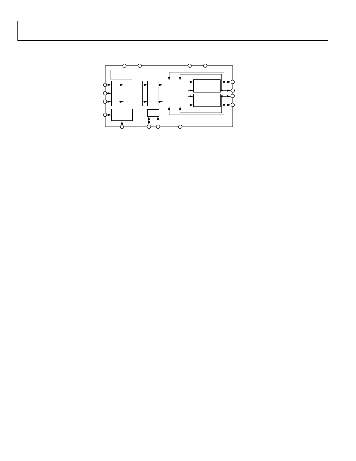
FUNCTIONAL BLOCK DIAGRAM
DVDD SA_MOD PVDD GND
POWER-ON
LRCLK
BCLK
SDATA
SD
RESET
VOLUME
2
CONTROL
I
S
CLOCKIN G
POWER
CONTROL
DRC
DAC
2
I
C
-
CLASS-D
MODULATOR
FULL BRIDGE
POWER
STAGE
FULL BRIDGE
POWER
STAGE
OUTL+
OUTL–
OUTR+
OUTR–
MCLK
SDA SCL
ADDR
10242-001
Figure 1.
Rev. A | Page 4 of 48
Data Sheet SSM2518
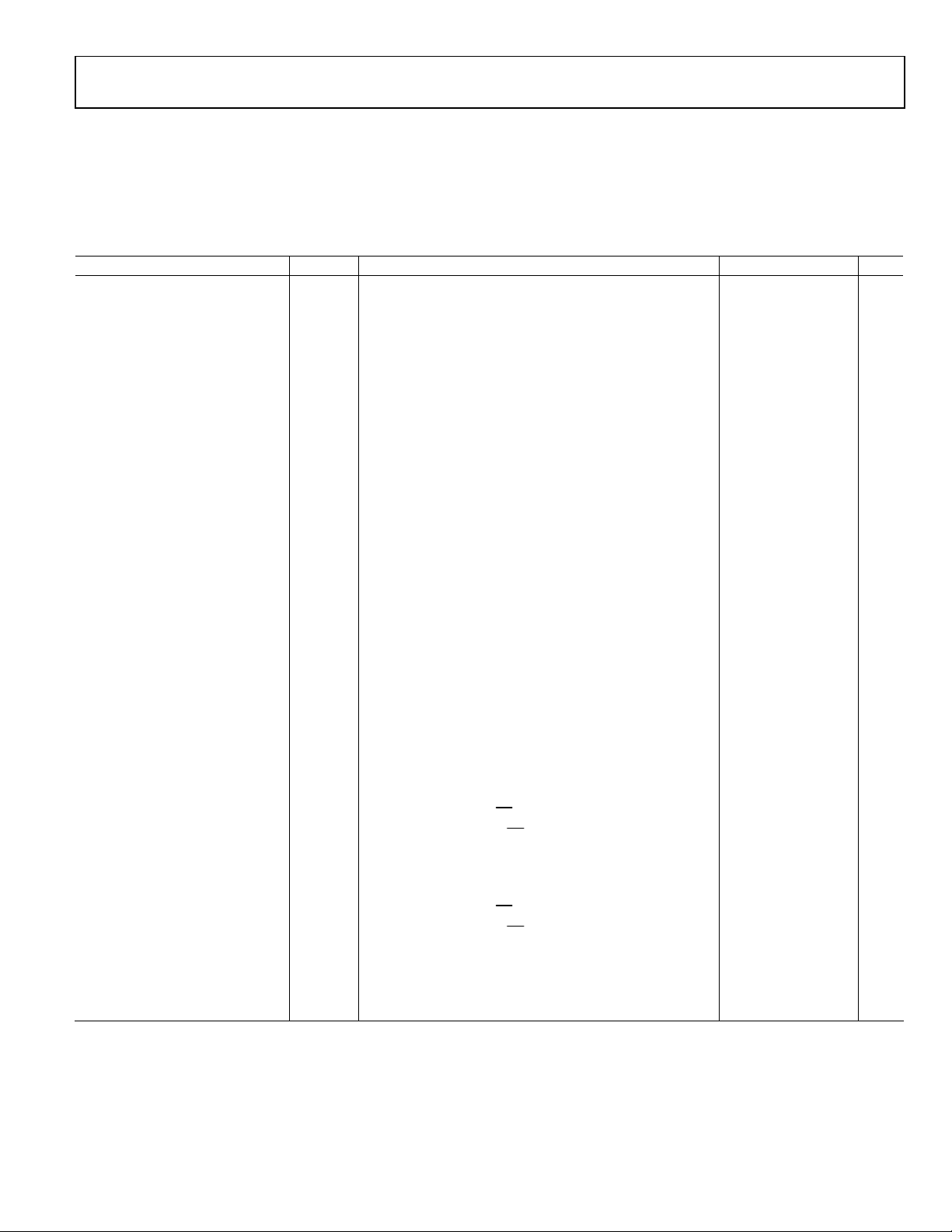
SPECIFICATIONS
All specifications at PVDD = 5.0 V, DVDD = 1.8 V, fS = 48 kHz, MCLK = 128 × fS, TA = 25°C, RL = 8 + 15 µH, LP_MODE = 0, volume
control = 0 dB, unless otherwise noted.
PERFORMANCE SPECIFICATIONS
Table 1.
Parameter Symbol Test Conditions/Comments Min Typ Max Unit
DEVICE CHARACTERISTICS
P
Output Power
R
R
R
R
R
R
R
R
R
R
R
Efficiency η PO = 1.4 W, 8 Ω, PVDD = 5.0 V, normal operation 91 %
P
Total Harmonic Distortion
Plus Noise
Channel Separation
Average Switching Frequency fSW 280 kHz
Differential Output Offset V
Power Supply Rejection Ratio PSRRDC PVDD = 2.5 V to 5.0 V 70 80 dB
PSRR
PSRR
Supply Current I
PVDD
Dither input, no load, PVDD = 3.6 V 4.4 mA
Dither input, no load, PVDD = 2.5 V 3.8 mA
DVDD I
Dither input, no load, DVDD = 1.8 V 1.5 mA
Dither input, no load, DVDD = 1.8 V, fS = 8 kHz 0.25 mA
Output Noise Voltage en PVDD = 5 V, f = 20 Hz to 20 kHz, dither input, A-weighted 50 μV
PVDD = 3.6 V, f = 20 Hz to 20 kHz, dither input, A-weighted 40 μV
Signal-to-Noise Ratio SNR A-weighted, referred to 0 dBFS, PVDD = 3.6 V 97 dB
Mute Attenuation Soft mute on 100 dB
f = 1 kHz, BW = 20 kHz
O
RL = 4 Ω, THD = 1%, PVDD = 5.0 V 2 W
= 4 Ω, THD = 10%, PVDD = 5.0 V 2.5 W
L
= 8 Ω, THD = 1%, PVDD = 5.0 V 1.42 W
L
= 8 Ω, THD = 10%, PVDD = 5.0 V 1.8 W
L
= 4 Ω, THD = 1%, PVDD = 3.6 V 1.3 W
L
= 4 Ω, THD = 10%, PVDD = 3.6 V 1.7 W
L
= 8 Ω, THD = 1%, PVDD = 3.6 V 0.75 W
L
= 8 Ω, THD = 10%, PVDD = 3.6 V 0.94 W
L
= 4 Ω, THD = 1%, PVDD = 2.5 V 0.4 W
L
= 4 Ω, THD = 10%, PVDD = 2.5 V 0.45 W
L
= 8 Ω, THD = 1%, PVDD = 2.5 V 0.275 W
L
= 8 Ω, THD = 10%, PVDD = 2.5 V 0.35 W
L
= 1.4 W, 8 Ω, PVDD = 5.0 V, ultralow EMI operation 86 %
O
THD + N PO = 0.5 W into 8 Ω each channel, f = 1 kHz, PVDD = 5 V 0.04 %
P
X
TAL K
OOS
GSM VRIPPLE
GSM VRIPPLE
PVDD
DVDD
= 0.25 W into 8 Ω each channel, f = 1 kHz, PVDD = 3.6 V 0.03 %
O
PO = 1 W, f = 1 kHz, PVDD = 5 V 108 dB
2.0 mV
= 100 mV rms at 217 Hz, dither input 80 dB
= 100 mV rms at 217 Hz, no input 100 dB
Dither input, no load, PVDD = 5.0 V 4.7 mA
Software power-down, SD
Hardware power-down, SD
= 1.8 V, SPWDN = 1, PVDD = 3.6 V
= 0 V, PVDD = 3.6 V
4 μA
100 nA
Dither input, no load, DVDD = 3.3 V 3.0 mA
Software power-down, SD
Hardware power-down, SD
= 1.8 V, SPWDN = 1, DVDD = 1.8 V
= 0 V, DVDD = 1.8 V
2.5 μA
100 nA
Rev. A | Page 5 of 48
SSM2518 Data Sheet
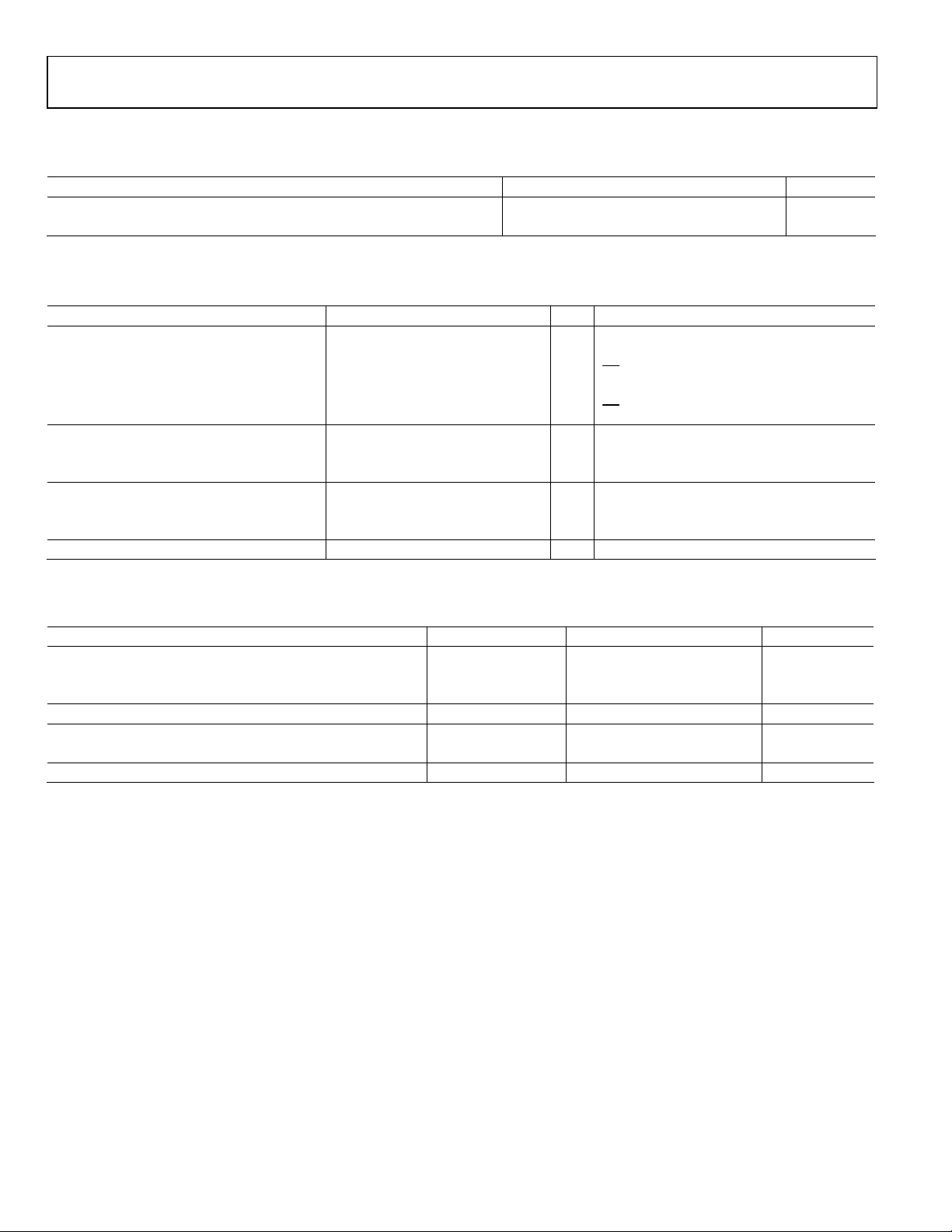
POWER SUPPLY REQUIREMENTS
Table 2.
Parameter Min Typ Max Unit
PVDD 2.5 3.6 5.5 V
DVDD 1.62 1.8 3.6 V
DIGITAL INPUT/OUTPUT
Table 3.
Parameter Min Typ Max Unit Test Conditions/Comments
INPUT VOLTAGE
High (VIH) 0.7 × DVDD 3.6 V ADDR, MCLK, BCLK, LRCLK, SDATA, SAMOD
1.35 5.5 V
Low (VIL) −0.3 +0.3 × DVDD V ADDR, MCLK, BCLK, LRCLK, SDATA, SAMOD
−0.3 +0.35 V
INPUT LEAKAGE CURRENT
High (IIH) 1 μA Excluding MCLK
Low (IIL) 1 μA Excluding MCLK and bidirectional pin
MCLK INPUT LEAKAGE CURRENT
High (IIH) 3 μA
Low (IIL) 3 μA
INPUT CAPACITANCE 5 pF
, SDA, SCL
SD
, SDA, SCL
SD
DIGITAL INTERPOLATION FILTER
Table 4.
Parameter Factor Min Typ1 Max Unit
PASS BAND
−3 dB 0.4535 × f
S
Ripple ±0.01 dB
TRANSITION BAND 0.5 × f
S
STOP BAND 0.5465 × fS 26 kHz
Attenuation 70 dB
GROUP DELAY 25/f
1
Typical value given for 48 kHz sample rate.
S
22 kHz
24 kHz
521 μs
Rev. A | Page 6 of 48
Data Sheet SSM2518
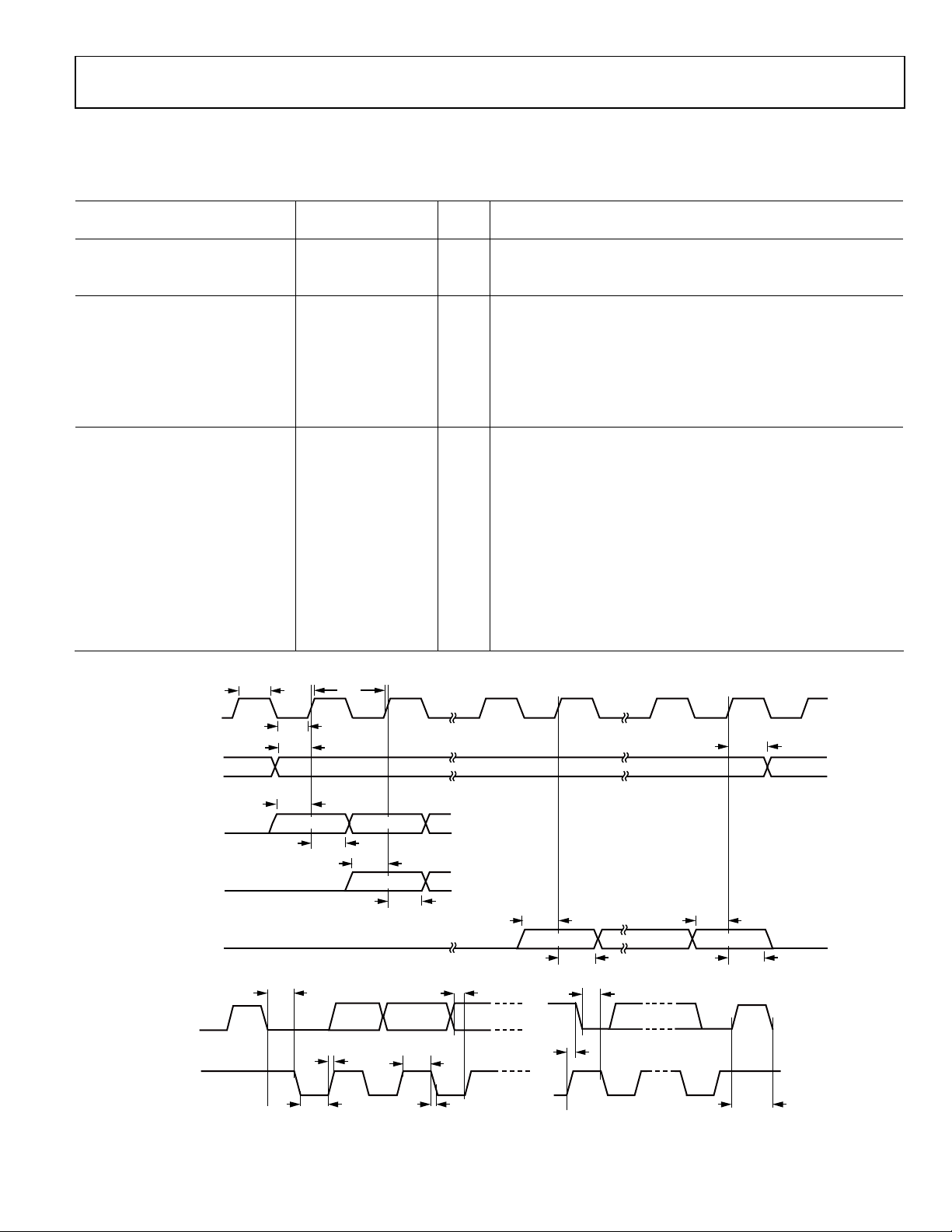
SDA
DIGITAL TIMING
All timing specifications are given for the default setting (I2S mode) of the serial input port.
Table 5.
Limit
Parameter Min Max Unit Description
MASTER CLOCK
tMP 74 136 ns MCLK period, 256 × fS mode (MCS = b0010)
tMP 148 271 ns MCLK period, 128 × fS mode (MCS = b0001)
SERIAL PORT
t
40 ns BCLK low pulse width
BIL
t
40 ns BCLK high pulse width
BIH
t
10 ns Setup time from LRCLK or SDATA edge to BCLK rising edge
LIS
t
10 ns Hold time from BCLK rising edge to LRCLK or SDATA edge
LIH
t
10 ns SDATA setup time to BCLK rising
SIS
t
10 ns SDATA hold time from BCLK rising
SIH
I2C PORT
f
SCL
t
0.6 μs SCL high
SCLH
t
1.3 μs SCL low
SCLL
t
0.6 μs Setup time; relevant for repeated start condition
SCS
t
0.6 μs Hold time; after this period, the first clock is generated
SCH
tDS 100 ns Data setup time
t
300 ns SCL rise time
SCR
t
300 ns SCL fall time
SCF
t
300 ns SDA rise time
SDR
t
300 ns SDA fall time
SDF
t
0.6 μs Bus-free time (time between stop and start)
BFT
400 kHz SCL frequency
Digital Timing Diagrams
BCLK
LRCLK
SDATA
LEFT-JUSTIFIED
MODE
SDATA
2
C-JUSTIFIED
I
MODE
RIGHT-JUSTIFIED
SDATA
MODE
SCL
t
BIH
START
CONDITION
t
BP
t
BIL
t
LIS
t
SIS
MSB
t
SIH
MSB – 1
t
SIS
MSB
t
SIH
t
SIS
MSB LSB
t
SIH
t
LIH
t
SIS
t
SIH
10242-002
Figure 2. Serial Input Port Timing
t
SCH
t
SCR
t
SCLL
t
DS
t
SCLH
t
SCF
Figure 3. I
2
C Port Timing
t
SCS
t
SCH
t
BFT
CONDITION
STOP
10242-003
Rev. A | Page 7 of 48
SSM2518 Data Sheet
v
ABSOLUTE MAXIMUM RATINGS
Absolute maximum ratings apply at 25°C, unless otherwise noted.
Table 6.
Parameter Rating
PVDD Supply Voltage −0.3 V to +6 V
DVDD Supply Voltage −0.3 V to +3.6 V
Input Voltage (ADDR, MCLK, BCLK, LRCLK,
SDATA, SAMOD Pins)
Input Voltage (SD, SDA, and SCL Pins)
ESD Susceptibility 4 kV
Storage Temperature Range −65°C to +150°C
Operating Temperature Range −40°C to +85°C
Junction Temperature Range −65°C to +165°C
Lead Temperature (Soldering, 60 sec) 300°C
Stresses abovethose listedunderAbsoluteMaximumRatings
may cause permanent damage to the device. This is a stress
rating only; functional operation of the device at these or any
other conditions above those indicated in the operational
section of this specification is not implied. Exposure to absolute
maximumratingconditionsfor extendedperiodsmayaffect
ice reliability.
de
−0.3 V to +3.6 V
−0.3 V to +6 V
THERMAL RESISTANCE
θJA is specified for the worst-case conditions, that is, a device
soldered in a circuit board for surface-mount packages.
Table 7. Thermal Resistance
Package Type θJA Unit
16-ball, 2 mm × 2 mm WLCSP 56 °C/W
20-lead, 4.0 mm × 4.0 mm LFCSP 54 °C/W
ESD CAUTION
Rev. A | Page 8 of 48
Data Sheet SSM2518
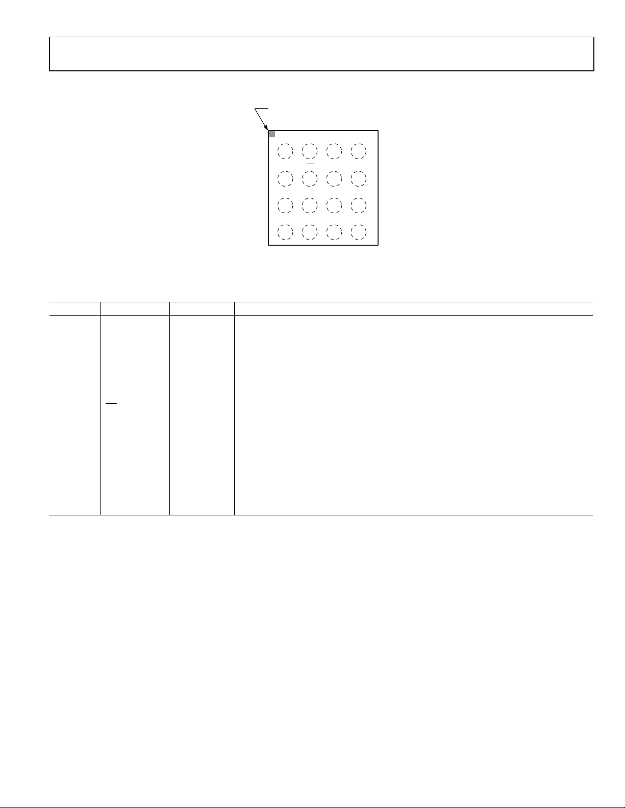
PIN CONFIGURATION AND FUNCTION DESCRIPTIONS
BALL A1
INDICAT OR
234
1
OUTR+
A
OUTR–
B
DVDD
C
SDATA
D
(BALL SIDE DOWN)
Figure 4. WLCSP Pin Configuration
Table 8. Pin Function Descriptions, WLCSP
Pin No. Mnemonic Function1 Description
A1 OUTR+ O Right Channel Output Positive.
B1 OUTR− O Right Channel Output Negative.
A4 OUTL+ O Left Channel Output Positive.
B4 OUTL− O Left Channel Output Negative.
A3 PVDD P 2.5 V to 5.5 V Amplifier Power.
A2 GND P Amplifier Ground.
C1 DVDD P 1.62 V to 3.6 V Digital and Analog Power.
B2
SD
I Power-Down Control, Active Low.
C3 SCL I I2C Clock.
C4 SDA I/O I2C Data.
D4 MCLK I Serial Audio Interface Master Clock.
D2 LRCLK I I2S Word Clock.
D3 BCLK I I2S Bit Clock.
D1 SDATA I I2S Serial Data.
C2 SAMOD I Standalone/I2C Mode Select. High = standalone mode, low = I2C mode.
B3 ADDR I I2C Address Select.
1
I is input, O is output, I/O is input/output, and P is power.
GND
SD
SAMOD
LRCLK
TOP VIEW
Not to Scale
PVDD
ADDR
SCL
BCLK
OUTL+
OUTL–
SDA
MCLK
10242-009
Rev. A | Page 9 of 48
SSM2518 Data Sheet
GND
GND
PVDD
20
1OUTL+
2OUTL–
SSM2518
3ADDR
TOP VIEW
4SDA
(Not to Scale)
5SCL
6
MCLK
NOTES
1. CONNECT THE EXPO S E D PAD TO GND.
Figure 5. LFCSP Pin Configuration
Table 9. Pin Function Descriptions, LFCSP
Pin No. Mnemonic Function1 Description
1 OUTL+ O Left Channel Output Positive.
2 OUTL− O Left Channel Output Negative.
3 ADDR I I2C Address Select.
4 SDA I/O I2C Data.
5 SCL I I2C Clock.
6 MCLK I Serial Audio Interface Master Clock.
7 BCLK I I2S Bit Clock.
8 GND P Amplifier Ground.
9 LRCLK I I2S Word Clock.
10 SDATA I I2S Serial Data.
11 SAMOD I Standalone/I2C Mode Select. High = standalone mode, low = I2C mode.
12 DVDD P 1.62 V to 3.6 V Digital and Analog Power.
13
SD
I Power-Down Control, Active Low.
14 OUTR− O Right Channel Output Negative.
15 OUTR+ O Right Channel Output Positive.
16 PVDD P 2.5 V to 5.5 V Amplifier Power.
17 GND P Amplifier Ground.
18 GND P Amplifier Ground.
19 GND P Amplifier Ground.
20 PVDD P 2.5 V to 5.5 V Amplifier Power.
1
I is input, O is output, I/O is input/output, and P is power.
GND
17
18
19
PIN 1
INDICATOR
9
8
7
GND
BCLK
LRCLK
PVDD
16
10
SDATA
15 OUTR+
14 OUTR–
13 SD
12 DVDD
11 SAMOD
10242-110
Rev. A | Page 10 of 48

Data Sheet SSM2518
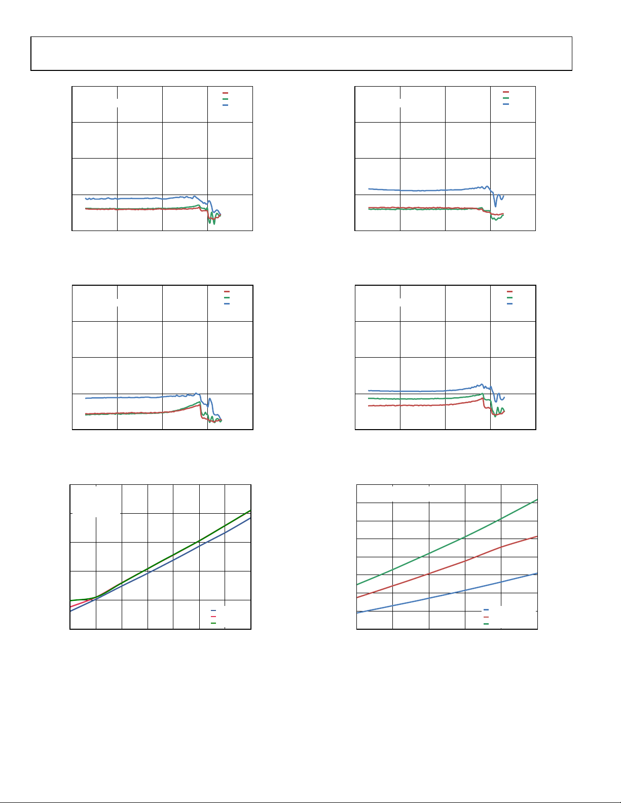
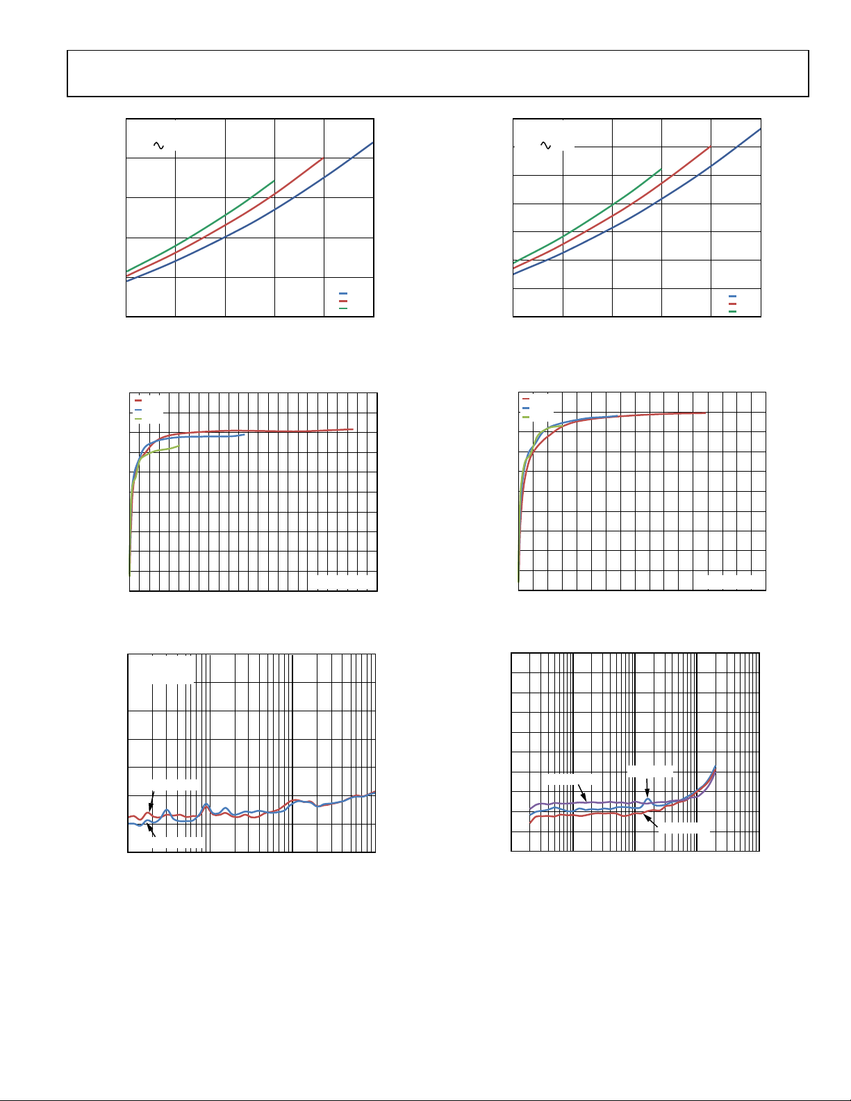
TYPICAL PERFORMANCE CHARACTERISTICS
100
GAIN = 5V
MCLK = 256 ×
RL = 8, 33µH
f
S
2.5V
3.6V
5.0V
100
GAIN = 3.6V
MCLK = 256 ×
RL = 8, 33µH
f
S
2.5V
3.6V
5.0V
10
1
THD + N (%)
0.1
0.01
0.001 0.01 0.1 1 10
OUTPUT POWER (W)
Figure 6. THD + N vs. Output Power into 8 Ω, 5.0 V Gain Setting
100
10
THD + N (%)
0.1
GAIN = 5V
MCLK = 256 ×
RL = 4, 15µH
1
f
S
2.5V
3.6V
5.0V
10
1
THD + N (%)
0.1
0.01
0.001 0.01 0.1 1 10
10242-011
OUTPUT POWE R (W)
10242-014
Figure 9. THD + N vs. Output Power into 8 Ω, 3.6 V Gain Setting
100
10
THD + N (%)
0.1
GAIN = 3.6V
MCLK = 256 ×
RL = 4, 15µH
1
f
S
2.5V
3.6V
5.0V
0.01
0.001 0.01 0.1 1 10
OUTPUT POWER (W)
Figure 7. THD + N vs. Output Power into 4 Ω, 5.0 V Gain Setting
100
PVDD = 5V
GAIN = 5V
MCLK = 256 ×
RL = 8, 33µH
10
1
THD + N (%)
0.1
0.01
10 100 1k 10k 100k
f
S
FREQUENCY (Hz)
Figure 8. THD + N vs. Frequency, PVDD = 5 V, R
0.25W
0.5W
1.0W
= 8 Ω
L
0.01
0.001 0. 01 0.1 1 10
10242-012
OUTPUT POWER (W)
10242-015
Figure 10. THD + N vs. Output Power into 4 Ω, 3.6 V Gain Setting
100
PVDD = 5V
GAIN = 5V
MCLK = 256 ×
RL = 4, 15µH
10
1
THD + N (%)
0.1
0.01
10 100 1k 10k 100k
10242-013
f
S
FREQUENCY (Hz)
Figure 11. THD + N vs. Frequency, PVDD = 5 V, R
0.25W
0.5W
1.0W
= 4 Ω
L
10242-016
Rev. A | Page 11 of 48
SSM2518 Data Sheet
100
PVDD = 3.6V
GAIN = 3.6V
MCLK = 256 ×
RL = 8, 33µH
10
0.125W
f
S
0.25W
0.5W
100
PVDD = 3.6V
GAIN = 3.6V
MCLK = 256 ×
RL = 4, 15µH
10
0.125W
f
S
0.25W
0.5W
1
THD + N (%)
0.1
0.01
10 100 1k 10k 100k
FREQUENCY (Hz)
Figure 12. THD + N vs. Frequency, PVDD = 3.6 V, R
100
PVDD = 2.5V
GAIN = 3.6V
MCLK = 256 ×
RL = 8, 33µH
10
1
THD + N (%)
0.1
0.01
10 100 1k 10k 100k
f
S
FREQUENC Y (Hz)
Figure 13. THD + N vs. Frequency, PVDD = 2.5 V, R
9
DAC_LPM = 1
AMP_LPM = 1
DVDD = 1.8V
DITHER INPUT
8
= 8 Ω
L
0.05W
0.10W
0.20W
= 8 Ω
L
1
THD + N (%)
0.1
0.01
10 100 1k 10k 100k
10242-017
Figure 15. THD + N vs. Frequency, PVDD = 3.6 V, R
FREQUENCY (Hz)
= 4 Ω
L
10242-020
100
PVDD = 2.5V
GAIN = 3.6V
MCLK = 256 ×
RL = 4, 15µH
10
1
THD + N (%)
0.1
0.01
10 100 1k 10k 100k
10242-018
f
S
FREQUENC Y (Hz)
Figure 16. THD + N vs. Frequency, PVDD = 2.5 V, R
0.05W
0.10W
0.20W
= 4 Ω
L
10242-021
4.0
MCLK = 256 ×
DAC_LPM = 1, AMP_L PM = 1
3.5
3.0
f
S
7
6
QUIESCENT CURRENT (mA)
5
4
2.5 3.0 3.5 4.0 4.5 5.0 5. 5 6.0
SUPPLY VOLTAGE (V)
NO LOAD
8 + 33µH
4 + 33µH
Figure 14. Quiescent Current (Power Stage) vs. Supply Voltage
10242-019
Rev. A | Page 12 of 48
2.5
2.0
1.5
1.0
QUIESCENT CURRENT (mA)
0.5
0
1.6 2.0 2.4 2.8 3.2 3.6
SUPPLY VOLTAGE (V)
8kHz 256 ×
24kHz 256 ×
48kHz 256 ×
Figure 17. Quiescent Current (Digital Core) vs. Supply Voltage
f
S
f
S
f
S
10242-022
Data Sheet SSM2518
2.5
2.0
1.5
GAIN = 5V
= 4, 15µH
R
L
1kHz
1.4
1.2
1.0
0.8
GAIN = 5V
= 8, 33µH
R
L
1kHz
1.0
OUTPUT POWER (W)
0.5
0
2.5 3. 0 3.5 4.0 4.5 5.0
SUPPLY VOLTAGE (V)
Figure 18. Maximum Output Power vs. Supply Voltage, R
100
5V
3.6V
90
2.5V
80
70
60
50
40
EFFICIENCY (%)
30
20
10
0
0 0.4 0.8 1.2 1.6 2.0 2.4 2.8 3.2 3.6 4.0 4.4 4.8
COMBINED OUTPUT POW ER, BOTH CHANNELS (W)
RL = 4, 15µ
Figure 19. Efficiency vs. Output Power into 4 Ω
0
PVDD = 5V
= 8, 33H
R
L
P
= 100mW
O
–20
–40
–60
–80
LEFT TO RIGHT
CROSSTALK (dB)
–100
–120
RIGHT TO LEFT
–140
20 200 2k
FREQUENC Y (Hz)
Figure 20. Crosstalk vs. Frequency
1%
5%
10%
= 4 Ω
L
20k
0.6
OUTPUT POWER ( W)
0.4
0.2
0
2.5 3.0 3.5 4.0 4.5 5.0
10242-024
SUPPLY VOLTAGE (V)
1%
5%
10%
10175-026
Figure 21. Maximum Output Power vs. Supply Voltage, RL = 8 Ω
100
5V
3.6V
90
2.5V
80
70
60
50
40
EFFICIENCY (%)
30
20
10
0
0 0.4 0.8 1.2 1.6 2.0 2.4 2.8 3.2
10242-028
COMBINED OUTPUT POW ER, BOTH CHANNELS (W)
RL = 8 + 33µ
10175-029
Figure 22. Efficiency vs. Output Power into 8 Ω
0
–10
–20
–30
–40
–50
PSRR (dB)
–60
–70
–80
–90
–100
10242-027
PVDD = 2.5V
10 100 1k 10k 100k
PVDD = 5V
FREQUENCY (Hz)
PVDD = 3.6V
10242-030
Figure 23. PSRR vs. Frequency
Rev. A | Page 13 of 48

SSM2518 Data Sheet
THEORY OF OPERATION
The SSM2518 is fully integrated 2-channel digital input, Class-D
output audio amplifier. The SSM2518 receives digital audio input
and produces the PDM differential switching outputs using the
internal power stage. The part has built in protection for overtemperature as well as overcurrent conditions. The SSM2518
also has built in soft turn on and soft turn off for pop-and-click
suppression. The part has programmable register control via the
2
I
C port.
POWER SUPPLIES
The SSM2518 requires two power supplies: PVDD and DVDD.
Descriptions of each of these supplies follow.
PVDD
The PVDD pin supplies power to the full bridge power stage
of a MOSFET and its associated drive, control, and protection
circuitry. PVDD can operate from 2.5 V to 5.5 V and must be
present to obtain audio output. Lowering the supply PVDD
results in lower output power and, correspondingly, lower
power consumption but does not degrade audio performance.
DVDD
The DVDD pin provides power to the digital logic circuitry and
determines the input trip points. DVDD can operate from 1.62 V
to 3.6 V and must be present to obtain audio output. Lowering
the supply voltage of DVDD results in lower power consumption but does not affect audio performance.
POWER-DOWN MODES
The SSM2518 offers a hardware shutdown pin, SD, which can
be used to set the IC to its lowest power state, with all blocks
disabled. This hardware shutdown mode is enabled when the
pin is pulled low.
SD
When the hardware shutdown is removed, the IC begins in
software power-down mode, where all blocks except for the
2
I
C interface are disabled. To fully power up the amplifier, clear
S_RST (Bit 7 of Register 0x00). In addition to the software
power-down, the software master mute is enabled at the initial
state of the amplifier; therefore, no audio is output until Bit 0 of
Register 0x07 is cleared.
The left and right channels can be independently shut down
by setting setting L_PWDN and R_PWDN (Bit 1 and Bit 2,
respectively, in Register 0x09). Disabling a channel shuts down
the channel specific digital processing, DAC, Class-D modulator,
and power stage.
The SSM2518 also contains a smart power-down feature, which
is enabled by default. This feature can be disabled by clearing
APWDN_EN (Bit 0 in Register 0x09). When active, this feature
monitors the incoming digital audio signal. If this is zero for
1024 consecutive samples, regardless of sample rate, it puts the
IC in the smart power-down state wherein all blocks, except the
2
I
S and I2C ports, are placed in a low power state. Once a single
nonzero input is received on the I
2
S interface, the SSM2518 leaves
this state and resumes normal operation.
POWER-ON RESET/VOLTAGE SUPERVISOR
The SSM2518 includes an internal power-on reset and voltage
supervisor circuit. This circuit provides an internal reset to all
circuitry whenever PVDD or DVDD is substantially below the
nominal operating threshold. This circuit simplifies supply
sequencing during initial power-on.
The circuit also monitors the power supplies to the SSM2518. If
the supply voltages fall below the nominal operating threshold,
this circuit stops the output and issues a reset. This ensures that
no damage occurs due to low voltage operation and that no pops
can occur under nearly any power removal condition.
MASTER AND BIT CLOCK
The SSM2518 requires an internal master clock to operate. This
clock must run at a frequency between 2.048 MHz and 6.144 MHz,
depending on the input sample rate, and it must be fully synchronous with the incoming audio data. This clock signal can be
derived from either the MCLK or BCLK pin, depending on the
configuration used.
If the MCLK pin is used, the internal clock is derived by either
dividing, passing through, or doubling the external clock signal
as required. The clock supplied to the MCLK pin can range from
2.048 MHz to 38.864 MHz. In this case, the external MCLK pin
signal can run at various multiples of the audio sample rate (f
The relationship between the MCLK rate and the audio sample
rate is determined by the master clock select (MCS) register setting,
Bits[4:1] in Register 0x00. Tab le 1 1 provides a summary of the
available options.
In addition, a bit clock must run at the same rate as the incoming
audio data on the SDATA pin. This clock can be supplied to the
BCLK pin, or it can be generated internally by dividing MCLK.
In this case, when BCLK_GEN (Bit 7 of Register 0x03) is set, the
logic level of the BCLK pin is used to select the audio interface
BCLK rate. Tie the BCLK pin to DVDD for 16 clock cycles per
channel; tie it to ground for 32 cycles per channel.
If the system bit clock is in the range of acceptable internal
master clock frequencies (between 2.048 MHz and 6.144 MHz),
then it can serve as both master clock and bit clock. Setting
NO_BCLK (Bit 5 of Register 0x00) routes the signal on the
).
S
Rev. A | Page 14 of 48

Data Sheet SSM2518
MCLK pin to serve as the internal bit clock as well. In this case,
tie the BCLK pin to ground.
Once the SSM2518 has entered its power-down state, it is
possible to gate the clocks to conserve system power. However, a
valid master clock must be present for the audio amplifier to
operate. It is best to use a low jitter clock (less than 1 ns peakto-peak) to ensure the specified audio performance.
Rev. A | Page 15 of 48

SSM2518 Data Sheet
TYPICAL APPLICATION CIRCUIT
AUDIO
PROCESSOR
1.35V TO 5. 5V
2.2k 2.2k
SYSTEM
MICROCONTROLLER
*OPTIONAL FO R APPLI CATIO NS WIT H >20cm SPEA KER CABLE.
Figure 24. Typical Application Circuit Using I
DVDD 1.62V TO 3. 6V
100nF
BCLK
LRCLK
SDATA
MCLK
SCL
SDA
SD
SAMOD
ADDR
DVDD
100nF
SSM2518
PVDD 2.5V TO 5. 5V
4.7µF
PVDD
OUTL+
OUTL–
OUTR+
OUTR–
GND
2
C Configuration
*
FB1
C1
470pF
FB2
C2
470pF
FB3
C3
470pF
FB4
C4
470pF
10242-039
Rev. A | Page 16 of 48

Data Sheet SSM2518
DIGITAL AUDIO INTERFACE
The SSM2518 operates as a slave on the serial audio interface.
2
It is capable of receiving stereo I
S-style, left justified, or right
justified data. Mono, stereo, and multichannel PCM/TDM
interface formats are available. The data format and interface
style are selected by adjusting the SDATA_FMT and SAI fields
in Register 0x02. Note that, when operating in right justified
mode, the proper data width must be chosen. The function of the
LRCLK pin varies depending on the data format. See Figure 26
through Figure 30 for the expected audio formats for various
configurations.
CHANNEL MAPPING
Stereo audio formats and TDM formats with 2, 4, 8, or 16
channels are available. In these modes, the amplifier left and
right audio can be independently chosen from any of the
available channels using the two fields in Register 0x04. For
most digital interface formats, many of these options are not
present. For example, in stereo modes, only Channel 0 and
Channel 1 are valid, and in four-slot TDM mode, only
Channel 0, Channel 1, Channel 2, and Channel 3 are valid.
SAMPLE RATE DETECTION
The SSM2518 can be configured to automatically detect the
sample rate, or the sample rate can be entered manually into the
FS field (Bit 1 and Bit 0 of Register 0x02). The choice of
automatic or manual sample rate detection is made by setting
the ASR bit (Bit 0 of Register 0x01). Sample rate detection
functions properly only when MCS (Bits[4:1] of Register 0x00)
is set correctly.
STANDALONE MODE
When the SAMOD pin is pulled high, the SSM2518 can operate
in several common stereo formats without any I
details of the serial audio interface can be configured by tying
the unused I
2
C pins to ground or DVDD, as shown in Tabl e 1 0 .
In addition, the amplifier gain can be controlled via the ADDR pin.
2
C control. Some
LOW POWER MODES
Two low power modes are available. If DAC_LPM (Bit 3 of
Register 0x09) is set, the digital-to-analog converter (DAC)
runs at half speed, reducing the quiescent current. This half
speed mode is also active when the MCS setting (Bits[4:1] of
Register 0x00) is set to its lowest value (MCS = 0000) because
the slowest acceptable MCLK rates can only support half speed
DAC operation.
If AMP_LPM (Bit 4 of Register 0x09) is set, the Σ- modulator
runs in a special mode that offers lower quiescent current when
the output power is small, at the expense of slightly degraded
audio performance.
DYNAMIC RANGE CONTROL
The dynamic range control, or DRC, can be used to reduce the
dynamic range of the audio signal. A common DRC scheme
involves applying a gain reduction to large output signals, along
with a net increase in gain for moderate to small signals. The
qualitative result is a louder speaker output for moderate output
levels without the undesired effects of amplifier clipping or
speaker overdrive at high levels.
To calculate the gain adjustment, an rms detector gives the
average level of the input signal, based on the averaging time set
by RMS_TAV (Bits[3:0] in Register 0x12). Based on this time
averaged level, the overall gain is adjusted so that the input/
output characteristic matches the specified compression curve.
This curve can be represented by a log-to-log graph with five
distinct regions, as shown in Figure 25.
NT ET CT LT
SMAX
CT
Table 10. Standalone Mode Pin Functions
Pin Standalone Function Pin Options
SCL FORMAT Low: I2S
High: left justified
SDA MCLK_SEL Low: MCLK = 256 × fS
High: MCLK = 384 × fS
SD SD
High: normal operation
ADDR GAIN Low: +12 dB digital gain
High: 0 dB digital gain
Low: shutdown/mute
In standalone mode, the volume control, dynamic range control,
and EMI control features are disabled. Automatic sample rate
detection and smart power-down are enabled. All other settings
are set to their default values.
Rev. A | Page 17 of 48
OUTPUT
WITHOUT DRC
WITH DRC
WITHOUT DRC
WITH DRC
INPUT
Figure 25. DRC Compression Curve: Log-to-Log Representation of the DRC
Output Level vs. Input Level
ET
SMIN
10242-032
From bottom left to top right, these regions (shown in red) are
the noise gate, expander, linear region, compressor, and limiter.
The control points between these regions can be set using the
DRC control registers (Register 0x0A through Register 0x12)
using the variable names (CT, ET, and so forth) as shown on the
plot axes in Figure 25. Each element can be individually enabled
using the LIM_EN, COMP_EN, EXP_EN, and NG_EN bits in

SSM2518 Data Sheet
Register 0x0A. The entire DRC function can be enabled or
disabled using DRC_EN (Bits[1:0] of Register 0x0A).
Linear Region
For input amplitudes between the DRC_ET and DRC_CT
thresholds, the DRC attenuation is set to zero, that is, the input is
passed straight through to the output. This is the region in the
center of the compression curve (see Figure 25) with a 1:1 slope,
where the input and output amplitude are the same.
Compressor
Above the input level set by DRC_CT (Bits[3:0] of Register 0x0C), the output amplitude does not rise as quickly as
the input. This provides a smooth transition to the limiter
region, where the output stops increasing altogether at the input
level set by DRC_LT (Bits[7:4] of Register 0x0C). At this point,
the output level is DRC_SMAX (Bits[7:4] of Register 0x0E).
Limiter
When the input level is above the input level set by DRC_LT,
the output level does not exceed the level given by DRC_SMAX
(Bits[7:4] of Register 0x0E). Instead, the overall gain is reduced
to maintain that level without clipping.
Expander
When the expander is enabled and the input level falls below
the level set by DRC_ET (Bits[7:4] of Register 0x0D), the output
level begins to decrease more rapidly than the input. This
provides a smooth transition to the noise gate, where
sufficiently small signals are blocked completely.
When the input signal falls to the level set by DRC_NT
(Bits[3:0] of Register 0x0D), the output level is set by
DRC_SMIN (Bits[3:0] of Register 0x0E).
Noise Gate
When the noise gate is enabled and the input signal level falls
below the threshold set by DRC_NT for a period of time, the
output is set to zero. Set this at a level lower than all signals of
interest to block the output in periods of silence.
The period of time for which the input level must remain
below the noise gate threshold prior to the output setting to
zero is determined by HDT_NG, Bits[3:0] of Register 0x10.
Attack and Decay Rates
To prevent audible distortion effects as the gain changes, the
time constants for the attack (gain reduction) and decay (gain
increase) are adjustable. The attack time is set by DRC_ATT
(Bits[7:4] of Register 0x0F), and the decay time is set by
DRC_DEC (Bits[3:0] of Register 0x0F).
Between attack and decay, a hold time is used to prevent rapid
switching between increased gain and decreased gain. The hold
time is set by HDT_NOR (Bits[7:4] of Register 0x10).
Post-DRC Gain
Because the DRC feature may have an overall effect on the
system gain, a separate digital gain option is provided to allow
the user to compensate for this effect. This digital gain option is
independent of the volume control feature, allowing an overall
gain adjustment that remains separate from the volume settings.
This level is set by DRC_POST_G (Bits[5:2] of Register 0x11).
Depending on the application, the entire DRC block can be placed
before or after the volume controls (L_VOL and R_VOL). This
option is set by PRE_VOL (Bit 6 of Register 0x0A).
MUTE OPTIONS
Several mute options are available. Each channel can be muted
independently using the left channel mute (L_MUTE, Bit 1 of
Register 0x07) or the right channel mute (R_MUTE, Bit 2 of
Register 0x07). Alternatively, both channels can be muted
simultaneously using the master mute option (M_MUTE, Bit 0
of Register 0x07).
The master mute is enabled at system startup; therefore, it must
be disabled before any audio is produced.
The SSM2518 also contains an automatic mute feature. This
feature is enabled by setting AMUTE (Bit 7 of Register 0x07).
When active, this feature monitors the incoming digital audio
signal. When the data stream is zero for 2048 consecutive
frames (1024 stereo samples), the output is muted. When a
single nonzero input is received on the I
SSM2518 is unmuted and resumes normal operation.
2
S interface, the
VOLUME CONTROL
The SSM2518 has a digital volume control that allows independent control of the left and right channels via Registers 0x05
and 0x06, respectively. 255 levels are available, providing a
range from +24 dB to −71.25 dB in 0.375 dB increments. This is
a soft volume control, meaning that the gain is adjusted continuously from one value to another. This continuously adjusted
gain prevents the audible pop that occurs with an instantaneous
gain adjustment.
When VOL_LINK (Bit 3 in Register 0x07) is set, both channels
are linked to the left channel volume setting.
DE-EMPHASIS FILTER
A digital de-emphasis filter is provided to compensate for the
standard compact disc style preemphasis, which occurs in some
audio systems. This filter is designed for use with a 44.1 kHz
sample rate only. To enable the de-emphasis filter, set
DEEMP_EN (Bit 4 of Register 0x07).
ANALOG GAIN
The analog gain of the SSM2518 amplifier is set by ANA_GAIN
(Bit 5 of Register 0x07). Each gain setting is designed to match
the scaling needed for a specified PVDD voltage so that the
digital full-scale values correspond to the clipping points of the
amplifier at that voltage.
If PVDD is larger than the voltage specified in this register, the
digital scale does not fill the output voltage range and maximum
output power is reduced. Similarly, if PVDD is smaller than
Rev. A | Page 18 of 48

Data Sheet SSM2518
specified in this register, analog clipping may occur within the
range of possible digital codes.
FAULT DETECTION AND RECOVERY
Three fault conditions are detected by the SSM2518 fault
detection system: left channel overcurrent, right channel
overcurrent, and overtemperature. When any of these is
detected, the amplifier shuts down and a read-only I
to indicate the cause of the shutdown. The OC_L, OC_R, and
OT fault indicators are Bit 7, Bit 6, and Bit 5 (respectively) of
Register 0x08.
An autorecovery feature can be enabled for temperature faults,
current faults, or both, depending on the state of ARCV (Bit 1
and Bit 0 of Register 0x08).
2
C bit is set
If autorecovery is enabled, the amplifier waits a short time
(10 ms, 20 ms, 40 ms, or 80 ms) and attempts to recover. The
recovery delay is set by AR_TIME (Bit 7 and Bit 6 of Register 0x09).
The maximum number of consecutive recovery attempts can be
set to one, three, seven, or unlimited attempts; this number is
set by MAX_AR (Bit 3 and Bit 2 of Register 0x08).
If the autorecovery feature is disabled or the maximum number
of attempts has been reached, the amplifier remains shut down
until a software reset or manual fault recovery attempt occurs.
The manual fault recovery is triggered by setting the write-only
bit, MRCV (Bit 4 of Register 0x08).
Rev. A | Page 19 of 48

SSM2518 Data Sheet
S
S
DIGITAL AUDIO FORMATS
STEREO MODE
SAI = 0
SDATA_FMT = 0 (I
BCLK
LRCLK
2
S), 1 (LJ), 2 (RJ 24-bit), 3 (RJ 16-bit)
ANY# BCLKs
SDATA I2S
SDATA LJ
SDATA RJ
LEFT CHANNEL
8 TO 32 BCLKs
RIGHT CHANNEL
8 TO 32 BCLKs
8 TO 32 BCLKs
Figure 26. Stereo Modes: I
TDM, 50% DUTY CYCLE MODE
SAI = 1 (2 slots), 2 (4 slots), 3 (8 slots), 4 (16 slots)
SDATA_FMT = 0 (I
BCLK_EDGE = 0
LRCLK_MODE = 0
SLOT_WIDTH = 0 (32 BCLKs), 1 (24 BCLKs), 2 (16 BCLKs)
BCLK
LRCLK
DATA I2S
SDATA LJ
SDATA RJ
2
S), 1 (LJ), 2 (RJ 24-bit), 3 (RJ 16-bit)
32/24/ 16 BCLKs 32/2 4/16 BCLKs 32/24/ 16 BCLKs
CHANNEL 1
8 TO 32 BCLKs
CHANNEL 1 CHANNEL 2
8 TO 32 BCLKs 8 TO 32 BCLKs 8 TO 32 BCLKs
CHANNEL 1
24 OR 16 BCLKs 24 O R 16 BCLKs 24 OR 16 BCLKs
Figure 27. TDM Modes with 50% Duty Cycle LRCLK
TDM, PULSE MODE
SAI = 1 (2 slots), 2 (4 slots), 3 (8 slots), 4 (16 slots)
SDATA_FMT = 0 (I
BCLK_EDGE = 0
LRCLK_MODE = 1
SLOT_WIDTH = 0 (32 BCLKs), 1 (24 BCLKs), 2 (16 BCLKs)
BCLK
LRCLK
2
S), 1 (LJ), 2 (RJ 24-bit), 3 (RJ 16-bit)
32/24/ 16 BCLKs 32/24 /16 BCLKs 32/24/1 6 BCLKs
RIGHT CHANNEL
8 TO 32 BCLKs
LEFT CHANNEL
8 TO 32 BCLKs
LEFT CHANNELRIGHT CHANNEL
8 TO 32 BCLKs
2
S, Left Justified, and Right Justified
CHANNEL 2
8 TO 32 BCLKs 8 TO 32 BCLKs
CHANNEL N
CHANNEL 2
CHANNEL N
CHANNEL N
10242-004
10242-005
DATA I2S
SDATA LJ
SDATA RJ
CHANNEL 1 CHANNEL 2
8 TO 32 BCLKs 8 TO 32 BCLKs 8 TO 32 BCLKs
CHANNEL 1
8 TO 32 BCLKs 8 TO 32 BCLKs 8 TO 32 BCLKs
CHANNEL 1
24 OR 16 BCLKs 24 O R 16 BCLKs 24 OR 16 BCLKs
CHANNEL 2
CHANNEL N
CHANNEL 2
CHANNEL N
CHANNEL N
10242-006
Figure 28. TDM Modes with Pulse Mode LRCLK
Rev. A | Page 20 of 48

Data Sheet SSM2518
S
PCM, MULTICHANNEL MODE
SAI = 1 (2 channels), 2 (4 channels), 3 (8 channels), 4 (16 channels)
SDATA_FMT = 0 (I
BCLK_EDGE = 1
LRCLK_MODE = 1
SLOT_WIDTH = 0 (32 BCLKs), 1 (24 BCLKs), 2 (16 BCLKs)
BCLK
LRCLK
2
S), 1 (LJ), 2 (RJ 24-bit), 3 (RJ 16-bit)
32/24/ 16 BCLKs32/24/ 16 BCLKs 32/24/ 16 BCLKs
DATA I2S
SDATA LJ
SDATA RJ
CHANNEL 1
8 TO 32 BCLKs
PCM MONO MODE
SAI = 5
SDATA_FMT = 0 (I
BCLK_EDGE = 1
LRCLK_MODE = 1
2
S), 1 (LJ), 2 (RJ 24-bit), 3 (RJ 16-bit)
8 TO 32 BCLKs
BCLK
LRCLK
SDATA I2S
SDATA LJ
SDATA RJ
CHANNEL 1
CHANNEL 2
8 TO 32 BCLKs 8 TO 32 BCLKs
CHANNEL 1
24 OR 16 BCLKs 24 OR 16 BCLKs 24 OR 16 BCLKs
CHANNEL 2
CHANNEL N
CHANNEL 2
CHANNEL N
8 TO 32 BCLKs8 TO 32 BCLKs
CHANNEL N
Figure 29. Multichannel PCM Modes
ANY # BCLKs
MONO CHANNE L
8 TO 32 BCLKs
MONO CHANNE L
8 TO 32 BCLKs
MONO CHANNE L
8 TO 32 BCLKs
Figure 30. Mono PCM Modes
10242-007
10242-008
Rev. A | Page 21 of 48

SSM2518 Data Sheet
I2C CONFIGURATION INTERFACE
OVERVIEW
The SSM2518 supports a 2-wire serial (I2C-compatible) microprocessor bus driving multiple peripherals. Two pins, serial data
(SDA) and serial clock (SCL), carry information between the
SSM2518 and the system I
is always a slave on the bus, meaning it cannot initiate a data
transfer. Each slave device is recognized by a unique device
address. The device address byte format is shown in Figure 31.
The address resides in the first seven bits of the I
LSB of this byte sets either a read or write operation.
Logic Level 1 corresponds to a read operation, and Logic Level 0
corresponds to a write operation. The full byte addresses are
shown in Figure 3, where the subaddresses are automatically
incremented at word boundaries and can be used for writing
large amounts of data to contiguous memory locations. This
increment happens automatically after a single word write
unless a stop condition is encountered. A data transfer is always
terminated by a stop condition.
Both SDA and SCL should have a 2.2 kΩ pull-up resistor on the
lines connected to them.
BIT 0 BIT 1 BIT 2 BIT 3 BIT 4 BIT 5 BIT 6 BIT 7
01101ADDR0R/W
Figure 31. I
Addressing
Initially, each device on the I2C bus is in an idle state,
monitoring the SDA and SCL lines for a start condition and
the proper address. The I
establishing a start condition, defined by a high-to-low transition
on SDA while SCL remains high. This indicates that an
address/data stream follows. All devices on the bus respond to
the start condition and shift the next eight bits (the 7-bit
address plus the R/
the transmitted address responds by pulling the data line low
during the ninth clock pulse. The device address is determined
by the state of the ADDR pin. This ninth bit is known as an
acknowledge bit. All other devices withdraw from the bus at
this point and return to the idle condition. The R/
determines the direction of the data. A Logic 0 on the LSB of
the first byte means that the master writes information to the
peripheral, whereas a Logic 1 means that the master reads
information from the peripheral after writing the subaddress
and repeating the start address. A data transfer takes place until
a stop condition is encountered. A stop condition occurs when
SDA transitions from low to high while SCL is held high. The
timing for the I
2
C port is shown in . Figure 3
2
C master controller. The SSM2518
2
C write. The
2
C Device Address Byte Format
2
C master initiates a data transfer by
W
bit) MSB first. The device that recognizes
W
bit
10242-033
Stop and start conditions can be detected at any stage during the
data transfer. If these conditions are asserted out of sequence with
normal read and write operations, the SSM2518 immediately
jumps to the idle condition. During a given SCL high period,
the user should issue only one start condition, one stop condition,
or a single stop condition followed by a single start condition. If
an invalid subaddress is issued by the user, the SSM2518 does
not issue an acknowledge and returns to the idle condition. If
the user exceeds the highest subaddress while in auto-increment
mode, one of two actions is taken. In read mode, the SSM2518
outputs the highest subaddress register contents until the master
device issues a no acknowledge, indicating the end of a read. A
no acknowledge condition is where the SDA line is not pulled
low on the ninth clock pulse of SCL. If the highest subaddress
location is reached while in write mode, the data for the invalid
byte is not loaded into any subaddress register, a no acknowledge
is issued by the SSM2518, and the part returns to the idle
condition.
I2C Read and Write Operations
Figure 33 shows the timing of a single word write operation.
Every ninth clock, the SSM2518 issues an acknowledge by
pulling SDA low.
Figure 34 shows the timing of a burst mode write sequence.
This figure shows an example where the target destination
registers are two bytes. The SSM2518 knows to increment its
subaddress register every byte because the requested subaddress
corresponds to a register or memory area with a byte word
length.
The timing of a single word read operation is shown in
Figure 35. Note that the first R/
W
bit is 0, indicating a write
operation. This is because the subaddress still needs to be
written to set up the internal address. After the
SSM2518
acknowledges the receipt of the subaddress, the master must
issue a repeated start command followed by the chip address
byte with the R/
W
bit set to 1 (read). This causes the
SSM2518
SDA to reverse and begin driving data back to the master. The
master then responds every ninth pulse with an acknowledge
pulse to the .
SSM2518
Figure 36 shows the timing of a burst mode read sequence. This
figure shows an example where the target destination registers
are two bytes. The SSM2518 knows to increment its subaddress
register every byte because the requested subaddress corresponds
to a register or memory area with a byte word length.
Rev. A | Page 22 of 48

Data Sheet SSM2518
SCK
(CONTINUED)
(CONTINUED)
SDA
START BY
MASTER
SCK
SDA
START
BIT
START
CHIP ADDRESS ACK BY
BIT
ACK ACKR/W
FRAME 1
CHIP ADDRESS BYTE
FRAME 3
DATA BYTE 1
Figure 32. I
START
BIT
CHIP ADDRESS
(7 BITS)
R/W = 0
Figure 33. Single-Word I
CHIP ADDRESS STOP
R/W = 0
ACK BY
SLAVE
SUBADDRESS
Figure 34. Burst Mode I
SUBADDRESS
R/W = 0
SLAVE
Figure 35. Single-Word I
ACK BY
SLAVE
ACK BY
SLAVE
2
C Read/Write Timing
SUBADDRESS
(8 BITS)
2
C Write Format
ACK BY
SLAVE
DATA-
WORD 1
2
C Write Format
START
BIT
2
CHIP ADDRESS
C Read Format
ACK BY
SLAVE
ACK BY
SLAVE
R/W = 1
WORD 2
FRAME 2
SUBADDRESS BYT E
FRAME 4
DATA BYTE 2
DATA BYTE 1
(8 BITS)
DATA-
ACK BY
SLAVE
ACK BY
SLAVE
DATA
BYTE 1
STOP
BIT
ACK BY
MASTER
BIT
ACKACK
STOP BY
MASTER
10242-035
10242-036
STOP
BIT
10242-037
10242-034
START
CHIP ADDRESS STOP
BIT
R/W = 0
ACK BY
SLAVE
SUBADDRESS
ACK BY
SLAVE
Figure 36. Burst Mode I
START
BIT
CHIP ADDRESS
R/W = 1
2
C Read Format
ACK BY
SLAVE
DATA-
WORD 1
ACK BY
MASTER
BIT
10242-038
Rev. A | Page 23 of 48

SSM2518 Data Sheet
MCLK Frequency Settings
Table 11. MCS Bit Field Setting: MCLK, Ratio, and Frequency
Input
Sample Rate
8 kHz Ratio 256 × fS 512 × fS 1024 × fS 1536 × fS 2048 × fS 3072 × fS 400 × fS 800 × fS 1600 × fS
MCLK 2.048 MHz 4.096 MHz 8.192 MHz 12.288 MHz 16.384 MHz 24.576 MHz 3.20 MHz 6.40 MHz 12.80 MHz
11.025 kHz Ratio 256 × fS 512 × fS 1024 × fS 1536 × fS 2048 × fS 3072 × fS 400 × fS 800 × fS 1600 × fS
MCLK 2.822 MHz 5.6448 MHz 11.2896 MHz 16.9344 MHz 22.5792 MHz 33.8688 MHz 4.41 MHz 8.82 MHz 17.64 MHz
12 kHz Ratio 256 × fS 512 × fS 1024 × fS 1536 × fS 2048 × fS 3072 × fS 400 × fS 800 × fS 1600 × fS
MCLK 3.072 MHz 6.144 MHz 12.288 MHz 18.432 MHz 24.576 MHz 38.864 MHz 4.80 MHz 9.60 MHz 19.20 MHz
16 kHz Ratio 128 × fS 256 × fS 384 × fS 768 × fS 1024 × fS 1536 × fS 200 × fS 400 × fS 800 × fS
MCLK 2.048 MHz 4.096 MHz 8.192 MHz 12.288 MHz 16.384 MHz 24.576 MHz 3.20 MHz 6.40 MHz 12.80 MHz
22.05 kHz Ratio 128 × fS 256 × fS 512 × fS 768 × fS 1024 × fS 1536 × fS 200 × fS 400 × fS 800 × fS
MCLK 2.822 MHz 5.6448 MHz 11.2896 MHz 16.9344 MHz 22.5792 MHz 33.8688 MHz 4.41 MHz 8.82 MHz 17.64 MHz
24 kHz Ratio 128 × fS 256 × fS 512 × fS 768 × fS 1024 × fS 1536 × fS 200 × fS 400 × fS 800 × fS
MCLK 3.072 MHz 6.144 MHz 12.288 MHz 18.432 MHz 24.576 MHz 38.864 MHz 4.80 MHz 9.60 MHz 19.20 MHz
32 kHz Ratio 64 × fS 128 × fS 256 × fS 384 × fS 512 × fS 768 × fS 100 × fS 200 × fS 400 × fS
MCLK 2.048 MHz 4.096 MHz 8.192 MHz 12.288 MHz 16.384 MHz 24.576 MHz 3.20 MHz 6.40 MHz 12.80 MHz
44.1 kHz Ratio 64 × fS 128 × fS 256 × fS 384 × fS 512 × fS 768 × fS 100 × fS 200 × fS 400 × fS
MCLK 2.822 MHz 5.6448 MHz 11.2896 MHz 16.9344 MHz 22.5792 MHz 33.8688 MHz 4.41 MHz 8.82 MHz 17.64 MHz
48 kHz Ratio 64 × fS 128 × fS 256 × fS 384 × fS 512 × fS 768 × fS 100 × fS 200 × fS 400 × fS
MCLK 3.072 MHz 6.144 MHz 12.288 MHz 18.432 MHz 24.576 MHz 38.864 MHz 4.80 MHz 9.60 MHz 19.20 MHz
96 kHz Ratio 64 × fS 64 × fS 128 × fS 192 × fS 256 × fS 384 × fS 50 × fS 100 × fS 200 × fS
MCLK 3.072 MHz 6.144 MHz 12.288 MHz 18.432 MHz 24.576 MHz 38.864 MHz 4.80 MHz 9.60 MHz 19.20 MHz
1
When using MCS = 0000, the chip automatically operates in low power mode.
Setting 0
1
b0000
Setting 1
b0001
Setting 2
b0010
Setting 3
b0011
Setting 4
b0100
Setting 5
b0101
Setting 6
b0110
Setting 7
b0111
Setting 8
b1000
Rev. A | Page 24 of 48

Data Sheet SSM2518
REGISTER SUMMARY (REG_MAP)
Table 12. REG_MAP Register Summary
Reg Name Bits Bit 7 Bit 6 Bit 5 Bit 4 Bit 3 Bit 2 Bit 1 Bit 0 Reset RW
0x00 Reset_Power_Control [7:0] S_RST RESERVED NO_BCLK MCS SPWDN 0x05 RW
0x01 Edge_Clock_Control [7:0] RESERVED EDGE ASR 0x00 RW
0x02 Serial_Interface_Sample_Rate_Control [7:0] RESERVED SDATA_FMT SAI FS 0x02 RW
0x03 Serial_Interface_Control [7:0] BCLK_GEN LRCLK_MODE LRCLK_POL SAI_MSB SLOT_WIDTH BCLK_EDGE RESERVED 0x00 RW
0x04 Channel_Mapping_Control [7:0] CH_SEL_R CH_SEL_L 0x10 RW
0x05 Left_Volume_Control [7:0] L_VOL 0x40 RW
0x06 Right_Volume_Control [7:0] R_VOL 0x40 RW
0x07 Volume_Mute_Control [7:0] AMUTE RESERVED ANA_GAIN DEEMP_EN VOL_LINK R_MUTE L_MUTE M_MUTE 0x81 RW
0x08 Fault_Control_1 [7:0] OC_L OC_R OT MRCV MAX_AR ARCV 0x0C RW
0x09 Power_Fault_Control [7:0] AR_TIME RESERVED AMP_LPM DAC_LPM R_PWDN L_PWDN APWDN_EN 0x99 RW
0x0A DRC_Control_1 [7:0] RESERVED PRE_VOL LIM_EN COMP_EN EXP_EN NG_EN DRC_EN 0x7C RW
0x0B DRC_Control_2 [7:0] PEAK_ATT PEAK_REL 0x5B RW
0x0C DRC_Control_3 [7:0] DRC_LT DRC_CT 0x57 RW
0x0D DRC_Control_4 [7:0] DRC_ET DRC_NT 0x89 RW
0x0E DRC_Control_5 [7:0] DRC_SMAX DRC_SMIN 0x8C RW
0x0F DRC_Control_6 [7:0] DRC_ATT DRC_DEC 0x77 RW
0x10 DRC_Control_7 [7:0] HDT_NOR HDT_NG 0x26 RW
0x11 DRC_Control_8 [7:0] RESERVED DRC_POST_G RESERVED 0x1C RW
0x12 DRC_Control_9 [7:0] RESERVED RMS_TAV 0x07 RW
Rev. A | Page 25 of 48

SSM2518 Data Sheet
REGISTER (REG_MAP) DETAILS
SOFTWARE RESET AND MASTER SOFTWARE POWER-DOWN CONTROL REGISTER
Address: 0x00, Reset: 0x05, Name: Reset_Power_Control
Table 13. Bit Descriptions for Reset_Power_Control
Bits Bit Name Settings Description Reset Access
7 S_RST
Software Reset. Write 1 to reset all internal blocks, including I
to their initial state.
0 Normal operation
1 Software reset
6 RESERVED Reserved. 0x0 RW
5 NO_BCLK
Bit Clock Source Selection. Either the MCLK or BCLK pin can be routed
internally to the bit clock.
0 BCLK pin used as bit clock source. Typical configuration.
1 MCLK pin used as bit clock source. No BCLK pin connection is needed.
[4:1] MCS
Master Clock Select. This must match the ratio between the input MCLK
frequency and the audio sample rate, as shown in Table 11.
0000 64 × fS
0001 128 × f
0010 256 × f
0011 384 × f
0100 512 × f
0101 768 × f
0110 100 × f
0111 200 × f
1000 400 × f
S
S
S
S
S
S
S
S
1001 Reserved
0 SPWDN
Software Master Power-Down. This places all blocks, except the I
interface, into a low power state.
0 Normal operation
1 Software master power-down
2
C registers,
2
C
0x0 RW
0x0 RW
0x2 RW
0x1 RW
Rev. A | Page 26 of 48

Data Sheet SSM2518
EDGE SPEED AND CLOCKING CONTROL REGISTER
Address: 0x01, Reset: 0x00, Name: Edge_Clock_Control
Table 14. Bit Descriptions for Edge_Clock_Control
Bits Bit Name Settings Description Reset Access
[7:3] RESERVED Reserved. 0x00 RW
[2:1] EDGE
00 No edge rate control
01 Low EMI
10 Lower EMI
11 Lowest EMI
0 ASR Automatic Sample Rate Detection. 0x0 RW
0 Automatic detection enabled
1 Manual sample rate selection given by FS field, Bits[1:0] of Register 0x02
Edge Rate Control. This limits the edge rate of the switching output stage.
The low EMI operation modes reduce the edge speed, lowering EMI and
power efficiency.
0x0 RW
Rev. A | Page 27 of 48

SSM2518 Data Sheet
SERIAL AUDIO INTERFACE AND SAMPLE RATE CONTROL REGISTER
Address: 0x02, Reset: 0x02, Name: Serial_Interface_Sample_Rate_Control
Table 15. Bit Descriptions for Serial_Interface_Sample_Rate_Control
Bits Bit Name Settings Description Reset Access
7 RESERVED Reserved. 0x0 RW
[6:5] SDATA_FMT Serial Data Format. Only required if SAI = 000. 0x0 RW
00 I²S standard; data is delayed by one BCLK cycle
01 Left justified
10 Right justified, 24-bit data
11 Right justified, 16-bit data
[4:2] SAI Serial Audio Interface Format. 0x0 RW
000 I2S, left justified, or right justified stereo (depending on SDATA_FMT)
001 2-slot TDM
010 4-slot TDM
011 8-slot TDM
100 16-slot TDM
101 Mono PCM
110 Reserved
111 Reserved
[1:0] FS Manual Sample Rate Selection. Only required if ASR = 1 in Register 0x01. 0x2 RW
00 8 kHz to 12 kHz
01 16 kHz to 24 kHz
10 32 kHz to 48 kHz
11 64 kHz to 96 kHz
Rev. A | Page 28 of 48

Data Sheet SSM2518
SERIAL AUDIO INTERFACE CONTROL REGISTER
Address: 0x03, Reset: 0x00, Name: Serial_Interface_Control
Table 16. Bit Descriptions for Serial_Interface_Control
Bits Bit Name Settings Description Reset Access
7 BCLK_GEN Internal BCLK Generator Enable. 0x0 RW
0 Bit clock from BCLK pin is used
1 Internally generated bit clock is used
6 LRCLK_MODE LRCLK Shape Selection. Required only for TDM modes. 0x0 RW
0 50% duty cycle
1 1-bit pulse
5 LRCLK_POL LRCLK Polarity. 0x0 RW
0 Rising edge (normal)
1 Falling edge (inverted)
4 SAI_MSB Serial Data Bit Order. 0x0 RW
0 MSB first
1 LSB first
[3:2] SLOT_WIDTH TDM Slot Width. Required only for TDM modes. 0x0 RW
00 32 BCLK cycles per slot
01 24 BCLK cycles per slot
10 16 BCLK cycles per slot
11 Reserved
1 BCLK_EDGE BCLK Active Edge. 0x0 RW
0 Rising BCLK edge used
1 Falling BCLK edge used
0 RESERVED Reserved. 0x0 RW
Rev. A | Page 29 of 48

SSM2518 Data Sheet
CHANNEL MAPPING CONTROL REGISTER
Address: 0x04, Reset: 0x10, Name: Channel_Mapping_Control
Table 17. Bit Descriptions for Channel_Mapping_Control
Bits Bit Name Settings Description Reset Access
[7:4] CH_SEL_R
Channel 0 to Channel 3 valid when running in 4-slot TDM mode.
Channel 0 to Channel 7 valid when running in 8-slot TDM mode.
Channel 0 to Channel 15 valid when running in 16-slot TDM mode.
0000 Channel 0
0001 Channel 1
0010 Channel 2
0011 Channel 3
0100 Channel 4
0101 Channel 5
0110 Channel 6
0111 Channel 7
1000 Channel 8
1001 Channel 9
1010 Channel 10
1011 Channel 11
1100 Channel 12
1101 Channel 13
1110 Channel 14
1111 Channel 15
[3:0] CH_SEL_L Left Channel Select. Channel 0 valid when running in mono (PCM) mode. 0x0 RW
Channel 0 to Channel 3 valid when running in 4-slot TDM mode.
Channel 0 to Channel 7 valid when running in 8-slot TDM mode.
Channel 0 to Channel 15 valid when running in 16-slot TDM mode.
0000 Channel 0
0001 Channel 1
Right Channel Select. Channel 0 valid when running in mono (PCM)
mode.
Channel 0 to Channel 1 valid when running in stereo and 2-slot TDM
modes.
Channel 0 to Channel 1 valid when running in stereo and 2-slot TDM
modes.
Rev. A | Page 30 of 48
0x1 RW

Data Sheet SSM2518
Bits Bit Name Settings Description Reset Access
0010 Channel 2
0011 Channel 3
0100 Channel 4
0101 Channel 5
0110 Channel 6
0111 Channel 7
1000 Channel 8
1001 Channel 9
1010 Channel 10
1011 Channel 11
1100 Channel 12
1101 Channel 13
1110 Channel 14
1111 Channel 15
LEFT CHANNEL VOLUME CONTROL REGISTER
Address: 0x05, Reset: 0x40, Name: Left_Volume_Control
Table 18. Bit Descriptions for Left_Volume_Control
Bits Bit Name Settings Description Reset Access
[7:0] L_VOL Left Channel Volume Control. Adjusts the digital gain in 0.375 dB
increments.
00000000 +24 dB
00000001 +23.625 dB
00000010 +23.35 dB
00000011 +22.875 dB
00000100 +22.5 dB
00000101 +22.125 dB
… …
00111111 +0.375 dB
01000000 0 dB
01000001 −0.375 dB
01000010 −0.750 dB
… …
11111101 −70.875 dB
11111110 −71.25 dB
11111111 Mute
Rev. A | Page 31 of 48
0x40 RW

SSM2518 Data Sheet
RIGHT CHANNEL VOLUME CONTROL REGISTER
Address: 0x06, Reset: 0x40, Name: Right_Volume_Control
Table 19. Bit Descriptions for Right_Volume_Control
Bits Bit Name Settings Description Reset Access
[7:0] R_VOL
00000000 +24 dB
00000001 +23.625 dB
00000010 +23.35 dB
00000011 +22.875 dB
00000100 +22.5 dB
00000101 +22.125 dB
… …
00111111 +0.375 dB
01000000 0 dB
01000001 −0.375 dB
01000010 −0.750 dB
… …
11111101 −70.875 dB
11111110 −71.25 dB
11111111 Mute
Right Channel Volume Control. Adjusts the digital gain in 0.375 dB
increments.
0x40 RW
Rev. A | Page 32 of 48

Data Sheet SSM2518
VOLUME AND MUTE CONTROL REGISTER
Address: 0x07, Reset: 0x81, Name: Volume_Mute_Control
Table 20. Bit Descriptions for Volume_Mute_Control
Bits Bit Name Settings Description Reset Access
7 AMUTE
0 Automute enabled
1 Automute disabled
6 RESERVED Reserved. 0x0 RW
5 ANA_GAIN
0 Matched to 3.6 V supply
1 Matched to 5.0 V supply
4 DEEMP_EN Digital De-Emphasis Filter. 0x0 RW
0 De-emphasis disabled (normal operation)
1 De-emphasis enabled
3 VOL_LINK
0 Normal operation
1 Both channels linked to L_VOL (Register 0x05)
2 R_MUTE Right Channel Soft Mute. 0x0 RW
0 Normal operation
1 Right channel muted
1 L_MUTE Left Channel Soft Mute. 0x0 RW
0 Normal operation
1 Left channel muted
0 M_MUTE Master Mute Control. This bit soft mutes both channels. 0x1 RW
0 Normal operation
1 Master mute
Automatic Mute Enable. After 2048 slots (1024 stereo samples) have been
received with zero data, the outputs mute until nonzero data arrives.
Analog Gain. This sets the full-scale output level of the amplifier. The two
settings are scaled appropriately for 3.6 V and 5.0 V nominal supply
voltages.
Volume Link. When this bit is enabled, both channels respond to the left
channel volume register.
0x1 RW
0x0 RW
0x0 RW
Rev. A | Page 33 of 48

SSM2518 Data Sheet
FAULT CONTROL 1 REGISTER
Address: 0x08, Reset: 0x0C, Name: Fault_Control_1
Table 21. Bit Descriptions for Fault_Control_1
Bits Bit Name Settings Description Reset Access
7 OC_L Left Channel Overcurrent Fault. Read only. 0x0 R
0 Normal operation
1 Left channel overcurrent fault
6 OC_R Right Channel Overcurrent Fault. Read only. 0x0 R
0 Normal operation
1 Right channel overcurrent fault
5 OT Overtemperature Fault Status. Read only. 0x0 R
0 Normal operation
1 Overtemperature fault
4 MRCV Manual Fault Recovery. Available only when ARCV = 11. Write only. 0x0 W
0 Normal operation
1 When written, attempt a manual fault recovery
[3:2] MAX_AR Maximum Fault Recovery Attempts. 0x3 RW
00 One attempt
01 Three attempts
10 Seven attempts
11 Unlimited attempts
[1:0] ARCV Automatic Fault Recovery Selection. 0x0 RW
00 Automatically recover from overtemperature and overcurrent faults
01 Automatically recover from overtemperature fault only
10 Automatically recover from overcurrent faults only
11 No automatic recovery
Rev. A | Page 34 of 48

Data Sheet SSM2518
POWER AND FAULT CONTROL REGISTER
Address: 0x09, Reset: 0x99, Name: Power_Fault_Control
Table 22. Bit Descriptions for Power_Fault_Control
Bits Bit Name Settings Description Reset Access
[7:6] AR_TIME
00 10 ms autorecovery delay
01 20 ms autorecovery delay
10 40 ms autorecovery delay
11 80 ms autorecovery delay
5 RESERVED Reserved. 0x0 RW
4 AMP_LPM Class-D Amplifier Low Power Mode. 0x1 RW
0 High performance operation
1 Low power operation
3 DAC_LPM DAC Low Power Mode. In low power mode, the DAC runs at half speed. 0x1 RW
0 Normal operation
1 Low power operation
2 R_PWDN Right Channel Power-Down. 0x0 RW
0 Normal operation
1 Right channel powered down
1 L_PWDN Left Channel Power-Down. 0x0 RW
0 Normal operation
1 Left channel powered down
0 APWDN_EN
0 Automatic power-down disabled
1 Automatic power-down enabled
Automatic Recovery Delay Time. This determines the amount of time
delay between fault detection and an autorecovery attempt.
Automatic Power-Down Enable. Automatic power-down automatically
puts the IC in a low power state when 2048 consecutive zero input
samples have been received.
0x2 RW
0x1 RW
Rev. A | Page 35 of 48

SSM2518 Data Sheet
DRC CONTROL 1 REGISTER
Address: 0x0A, Reset: 0x7C, Name: DRC_Control_1
Table 23. Bit Descriptions for DRC_Control_1
Bits Bit Name Settings Description Reset Access
7 RESERVED Reserved. 0x0 RW
6 PRE_VOL
0 DRC operates after the volume control
1 DRC operates before the volume control
5 LIM_EN
0 Limiter disabled
1 Limiter enabled
4 COMP_EN
0 Compressor disabled
1 Compressor enabled
3 EXP_EN
0 Expander disabled
1 Expander enabled
2 NG_EN
0 Noise gate disabled
1 Noise gate enabled
[1:0] DRC_EN
00 DRC disabled
01 Left channel DRC enabled
10 Right channel DRC enabled
11 Left and right channel DRC enabled
DRC Placement. This determines the placement of the DRC block in the
signal chain. When placed before the volume control, the thresholds are
relative to the input signal. When placed after the volume control, the
thresholds are relative to the output signal level. All thresholds are 6 dB
higher when placed after the volume control.
Limiter Enable. With the limiter enabled, the DRC_LT threshold (Bits[7:4] in
Register 0x0C) must be set.
Compressor Enable. With the compressor enabled, the DRC_CT and
DRC_SMAX thresholds (Bits[3:0] in Register 0x0C and Bits[7:4] in
Register 0x0E) must be set.
Expander Enable. With the expander enabled, the DRC_ET and DRC_SMIN
threshold values (Bits[7:4] in Register 0x0D and Bits[3:0] in Register 0x0E)
must be set.
Noise Gate Enable. With the noise gate enabled, the DRC_NT threshold
value (Bits[3:0] in Register 0x0D) must be set.
Master DRC Enable. This must be enabled for any of the DRC features to
function.
0x1 RW
0x1 RW
0x1 RW
0x1 RW
0x1 RW
0x0 RW
Rev. A | Page 36 of 48

Data Sheet SSM2518
DRC CONTROL 2 REGISTER
Address: 0x0B, Reset: 0x5B, Name: DRC_Control_2
Table 24. Bit Descriptions for DRC_Control_2
Bits Bit Name Settings Description Reset Access
[7:4] PEAK_ATT DRC Peak Detector Attack Time. 0x5 RW
0000 0 ms
0001 0.09 ms
0010 0.19 ms
0011 0.37 ms
0100 0.75 ms
0101 1.5 ms
0110 3 ms
0111 6 ms
1000 12 ms
1001 24 ms
1010 48 ms
1011 96 ms
1100 192 ms
1101 384 ms
1110 768 ms
1111 1.536 sec
[3:0] PEAK_REL DRC Peak Detector Release Time. 0xB RW
0000 0 ms
0001 1.5 ms
0010 3 ms
0011 6 ms
0100 12 ms
0101 24 ms
0110 48 ms
0111 96 ms
Rev. A | Page 37 of 48

SSM2518 Data Sheet
Bits Bit Name Settings Description Reset Access
1000 193 ms
1001 384 ms
1010 768 ms
1011 1.536 sec
1100 3.072 sec
1101 6.144 sec
1110 12.288 sec
1111 24.576 sec
DRC CONTROL 3 REGISTER
Address: 0x0C, Reset: 0x57, Name: DRC_Control_3
Table 25. Bit Descriptions for DRC_Control_3
Bits Bit Name Settings Description Reset Access
[7:4] DRC_LT DRC Limiter Threshold Setting. Relative to input. 0x5 RW
0000 0 dB
0001 −1 dB
0010 −2 dB
0011 −3 dB
0100 −4 dB
0101 −5 dB
0110 −6 dB
0111 −7 dB
1000 −8 dB
1001 −10 dB
1010 −12 dB
1011 −14 dB
1100 −16 dB
1101 −18 dB
1110 −20 dB
1111 −22 dB
Rev. A | Page 38 of 48

Data Sheet SSM2518
Bits Bit Name Settings Description Reset Access
[3:0] DRC_CT DRC Compressor Lower Threshold Setting. Relative to input. 0x7 RW
0000 −4 dB
0001 −6 dB
0010 −8 dB
0011 −10 dB
0100 −12 dB
0101 −14 dB
0110 −16 dB
0111 −18 dB
1000 −20 dB
1001 −22 dB
1010 −24 dB
1011 −26 dB
1100 −28 dB
1101 −30 dB
1110 −32 dB
1111 −34 dB
Rev. A | Page 39 of 48

SSM2518 Data Sheet
DRC CONTROL 4 REGISTER
Address: 0x0D, Reset: 0x89, Name: DRC_Control_4
Table 26. Bit Descriptions for DRC_Control_4
Bits Bit Name Settings Description Reset Access
[7:4] DRC_ET DRC Expander Upper Threshold Setting. Relative to input. 0x8 RW
0000 −36 dB
0001 −39 dB
0010 −42 dB
0011 −45 dB
0100 −48 dB
0101 −51 dB
0110 −54 dB
0111 −57 dB
1000 −60 dB
1001 −63 dB
1010 −66 dB
1011 −69 dB
1100 −72 dB
1101 −75 dB
1110 −78 dB
1111 −81 dB
[3:0] DRC_NT DRC Noise Gate Threshold Setting. Relative to input. 0x9 RW
0000 −51 dB
0001 −54 dB
0010 −57 dB
0011 −60 dB
0100 −63 dB
0101 −66 dB
0110 −69 dB
0111 −72 dB
1000 −75 dB
1001 −78 dB
1010 −81 dB
1011 −84 dB
Rev. A | Page 40 of 48

Data Sheet SSM2518
Bits Bit Name Settings Description Reset Access
1100 −87 dB
1101 −90 dB
1110 −93 dB
1111 −96 dB
DRC CONTROL 5 REGISTER
Address: 0x0E, Reset: 0x8C, Name: DRC_Control_5
Table 27. Bit Descriptions for DRC_Control_5
Bits Bit Name Settings Description Reset Access
[7:4] DRC_SMAX DRC Limiter Threshold Setting. Relative to input. 0x8 RW
0000 0 dB
0001 −1 dB
0010 −2 dB
0011 −3 dB
0100 −4 dB
0101 −5 dB
0110 −6 dB
0111 −7 dB
1000 −8 dB
1001 −10 dB
1010 −12 dB
1011 −14 dB
1100 −16 dB
1101 −18 dB
1110 −20 dB
1111 −22 dB
Rev. A | Page 41 of 48

SSM2518 Data Sheet
Bits Bit Name Settings Description Reset Access
[3:0] DRC_SMIN
0000 −51 dB
0001 −54 dB
0010 −57 dB
0011 −60 dB
0100 −63 dB
0101 −66 dB
0110 −69 dB
0111 −72 dB
1000 −75 dB
1001 −78 dB
1010 −81 dB
1011 −84 dB
1100 −87 dB
1101 −90 dB
1110 −93 dB
1111 −96 dB
DRC Minimum Output Signal Amplitude Setting. This is the minimum
output level produced by the DRC and is used to indicate the expander
lower threshold, or output signal level when the input rises beyond the
noise gate threshold.
0xC RW
DRC CONTROL 6 REGISTER
Address: 0x0F, Reset: 0x77, Name: DRC_Control_6
Table 28. Bit Descriptions for DRC_Control_6
Bits Bit Name Settings Description Reset Access
[7:4] DRC_ATT
0000 0 ms
0001 0.1 ms
0010 0.19 ms
0011 0.37 ms
0100 0.75 ms
0101 1.5 ms
DRC Attack Time. Used to smooth the gain curve at the thresholds (knees)
of each DRC function.
0x7 RW
Rev. A | Page 42 of 48

Data Sheet SSM2518
Bits Bit Name Settings Description Reset Access
0110 3 ms
0111 6 ms
1000 12 ms
1001 24 ms
1010 48 ms
1011 96 ms
1100 192 ms
1101 384 ms
1110 768 ms
1111 1.536 sec
[3:0] DRC_DEC
0000 0 ms
0001 1.5 ms
0010 3 ms
0011 6 ms
0100 12 ms
0101 24 ms
0110 48 ms
0111 96 ms
1000 192 ms
1001 384 ms
1010 768 ms
1011 1.536 sec
1100 3.072 sec
1101 6.144 sec
1110 12.288 sec
1111 24.576 sec
DRC Decay Time. Used to smooth the gain curve at the thresholds (knees)
of each DRC function.
0x7 RW
Rev. A | Page 43 of 48

SSM2518 Data Sheet
DRC CONTROL 7 REGISTER
Address: 0x10, Reset: 0x26, Name: DRC_Control_7
Table 29. Bit Descriptions for DRC_Control_7
Bits Bit Name Settings Description Reset Access
[7:4] HDT_NOR
0000 0 ms
0001 0.67 ms
0010 1.33 ms
0011 2.67 ms
0100 5.33 ms
0101 10.66 ms
0110 21.32 ms
0111 42.64 ms
1000 85.28 ms
1001 170.56 ms
1010 341.12 ms
1011 682.24 ms
1100 1.364 sec
1101 Reserved
1110 Reserved
1111 Reserved
[3:0] HDT_NG
0000 0 ms
0001 0.67 ms
0010 1.33 ms
0011 2.67 ms
0100 5.33 ms
0101 10.66 ms
0110 21.32 ms
0111 42.64 ms
1000 85.28 ms
1001 170.56 ms
DRC Normal Operation Hold Time. Used to prevent the gain curve
calculation from increasing too quickly.
DRC Noise Gate Hold Time. Used to prevent the DRC from entering noise
gate too quickly.
0x2 RW
0x6 RW
Rev. A | Page 44 of 48

Data Sheet SSM2518
Bits Bit Name Settings Description Reset Access
1010 341.12 ms
1011 682.24 ms
1100 1.364 sec
1101 Reserved
1110 Reserved
1111 Reserved
DRC CONTROL 8 REGISTER
Address: 0x11, Reset: 0x1C, Name: DRC_Control_8
Table 30. Bit Descriptions for DRC_Control_8
Bits Bit Name Settings Description Reset Access
[7:6] RESERVED Reserved. 0x0 RW
[5:2] DRC_POST_G
0000 +21 dB
0001 +18 dB
0010 +15 dB
0011 +12 dB
0100 +9 db
0101 +6 dB
0110 +3 dB
0111 0 dB
1000 −3 dB
1001 −6 dB
1010 −9 dB
1011 −12 dB
1100 −15 dB
1101 −18 dB
1110 −21 dB
1111 −24 dB
[1:0] RESERVED Reserved. 0x0 RW
Post-DRC Gain Adjust Setting. This can be used to add additional gain
after the DRC function to compensate for the overall reduction of system
gain due to the DRC.
0x7 RW
Rev. A | Page 45 of 48

SSM2518 Data Sheet
DRC CONTROL 9 REGISTER
Address: 0x12, Reset: 0x07, Name: DRC_Control_9
Table 31. Bit Descriptions for DRC_Control_9
Bits Bit Name Settings Description Reset Access
[7:4] RESERVED Reserved. 0x0 RW
[3:0] RMS_TAV
0000 0 ms
0001 1.5 ms
0010 3 ms
0011 6 ms
0100 12 ms
0101 24 ms
0110 48 ms
0111 96 ms
1000 192 ms
1001 384 ms
1010 768 ms
1011 1.536 sec
1100 3.072 sec
1101 6.144 sec
1110 12.288 sec
1111 24.576 sec
DRC RMS Detector Averaging Time. This is the averaging time for the rms
level that is compared to the DRC thresholds.
0x7 RW
Rev. A | Page 46 of 48

Data Sheet SSM2518
PACKAGING AND ORDERING INFORMATION
OUTLINE DIMENSIONS
2.250
2.210 SQ
2.170
3
2
4
1
PIN 1
INDICATOR
0.80
0.75
0.70
SEATING
PLANE
BALL 1
IDENTIFIER
0.660
0.600
0.540
SEATING
PLANE
1.50
REF
0.50
TOP VIEW
(BALL SI DE DOWN)
SIDE VIEW
0.360
0.320
0.280
REF
COPLANARITY
0.05
0.270
0.240
0.210
BOTTOM VIEW
(BALL SI DE UP)
Figure 37.16-Ball Wafer Level Chip Scale Package [WLCSP]
(CB-16-13)
Dimensions shown in millimeters
4.10
4.00 SQ
3.90
0.50
BSC
0.50
0.40
0.30
0.05 MAX
0.02 NOM
0.20 REF
COPLANARITY
0.08
0.30
0.25
0.20
16
15
EXPOSED
PAD
11
10
BOTTOM VIEWTOP VIEW
FOR PROPER CONNECTION OF
THE EXPOSED PAD, REFER TO
THE PIN CONFIGURATION AND
FUNCTION DESCRIPTIONS
SECTION OF THIS DATA SHEET.
A
B
C
D
05-19-2011-A
1
P
N
I
R
O
T
D
C
I
A
N
I
20
1
2.65
2.50 SQ
5
6
2.35
0.25 MIN
COMPLIANTTOJEDEC STANDARDS MO-220-WGGD.
Figure 38. 20-Lead Lead Frame Chip Scale Package [LFCSP_WQ]
4 mm × 4 mm Body, Very Very Thin Quad (CP-20-10)
Dimensions shown in millimeters
Rev. A | Page 47 of 48
061609-B

SSM2518 Data Sheet
ORDERING GUIDE
Model1 Temperature Range Package Description Package Option
SSM2518CBZ-RL −40°C to +85°C 16-Ball, 2.2 mm × 2.2 mm WLCSP CB-16-13
SSM2518CBZ-R7 −40°C to +85°C 16-Ball, 2.2 mm × 2.2 mm WLCSP CB-16-13
SSM2518CPZ −40°C to +85°C 20-Lead 4 mm × 4 mm LFCSP
SSM2518CPZ-R7 −40°C to +85°C 20-Lead 4 mm × 4 mm LFCSP
SSM2518CPZ-RL −40°C to +85°C 20-Lead 4 mm × 4 mm LFCSP
EVAL-SSM2518Z Evaluation Board
1
Z = RoHS Compliant Part.
CP-20-10
CP-20-10
CP-20-10
©2011 Analog Devices, Inc. All rights reserved. Trademarks and
registered trademarks are the prop erty of their respective owners.
D10242-0-12/11(A)
Rev. A | Page 48 of 48
www.analog.com/SSM2518
 Loading...