

Filterless High Efficiency
www.BDTIC.com/ADI
FEATURES
Filterless Class-D amplifier with Σ-Δ modulation
Automatic level control (ALC) improves dynamic range and
prevents clipping
3 W into 3 Ω load and 1.4 W into 8 Ω load at 5.0 V supply
with <10% total harmonic distortion (ALC off)
700 mW into 8 Ω load at 4.2 V supply (ALC 80%)
93% efficiency at 5.0 V, 1.4 W into 8 Ω speaker
>93 dB signal-to-noise ratio (SNR)
Single-supply operation from 2.5 V to 5.5 V
20 nA ultralow shutdown current
Short-circuit and thermal protection
Available in 9-ball, 1.5 mm × 1.5 mm WLCSP
Pop-and-click suppression
Built-in resistors reduce board component count
Default fixed 18 dB or user-adjustable gain setting
APPLICATIONS
Mobile phones
MP3 players
Portable gaming
Portable electronics
Educational toys
GENERAL DESCRIPTION
The SSM2317 is a fully integrated, high efficiency, Class-D audio
amplifier. It is designed to maximize performance for mobile
phone applications. The application circuit requires a minimum
of external components and operates from a single 2.5 V to 5.5 V
Mono 3 W Class-D Audio Amplifier
SSM2317
supply. It is capable of delivering 3 W of continuous output
power with <1% THD + N driving a 3 Ω load from a 5.0 V supply.
The SSM2317 features a high efficiency, low noise modulation
scheme that does not require any external LC output filters. The
modulation continues to provide high efficiency even at low output
power. It operates with 93% efficiency at 1.4 W into 8 Ω or 85%
efficiency at 3 W into 3 Ω from a 5.0 V supply and has an SNR of
>93 dB. Spread-spectrum pulse density modulation is used to
provide lower EMI radiated emissions compared with other
Class-D architectures.
Automatic level control (ALC) can be activated to suppress
clipping and improve dynamic range. This feature only requires
one external resistor tied to GND via the VTH pin and an
activation voltage on the ALC_EN pin.
The SSM2317 has a micropower shutdown mode with a typical
shutdown current of 20 nA. Shutdown is enabled by applying
a logic low to the
The device also includes pop-and-click suppression circuitry. This
minimizes voltage glitches at the output during turn-on and turnoff, reducing audible noise on activation and deactivation.
The default gain of the SSM2317 is 18 dB, but users can reduce the
gain by using a pair of external resistors (see the Gain section).
The SSM2317 is specified over the commercial temperature range
of −40°C to +85°C. It has built-in thermal shutdown and output
short-circuit protection. It is available in a 9-ball, 1.5 mm × 1.5 mm
wafer level chip scale package (WLCSP).
SD
pin.
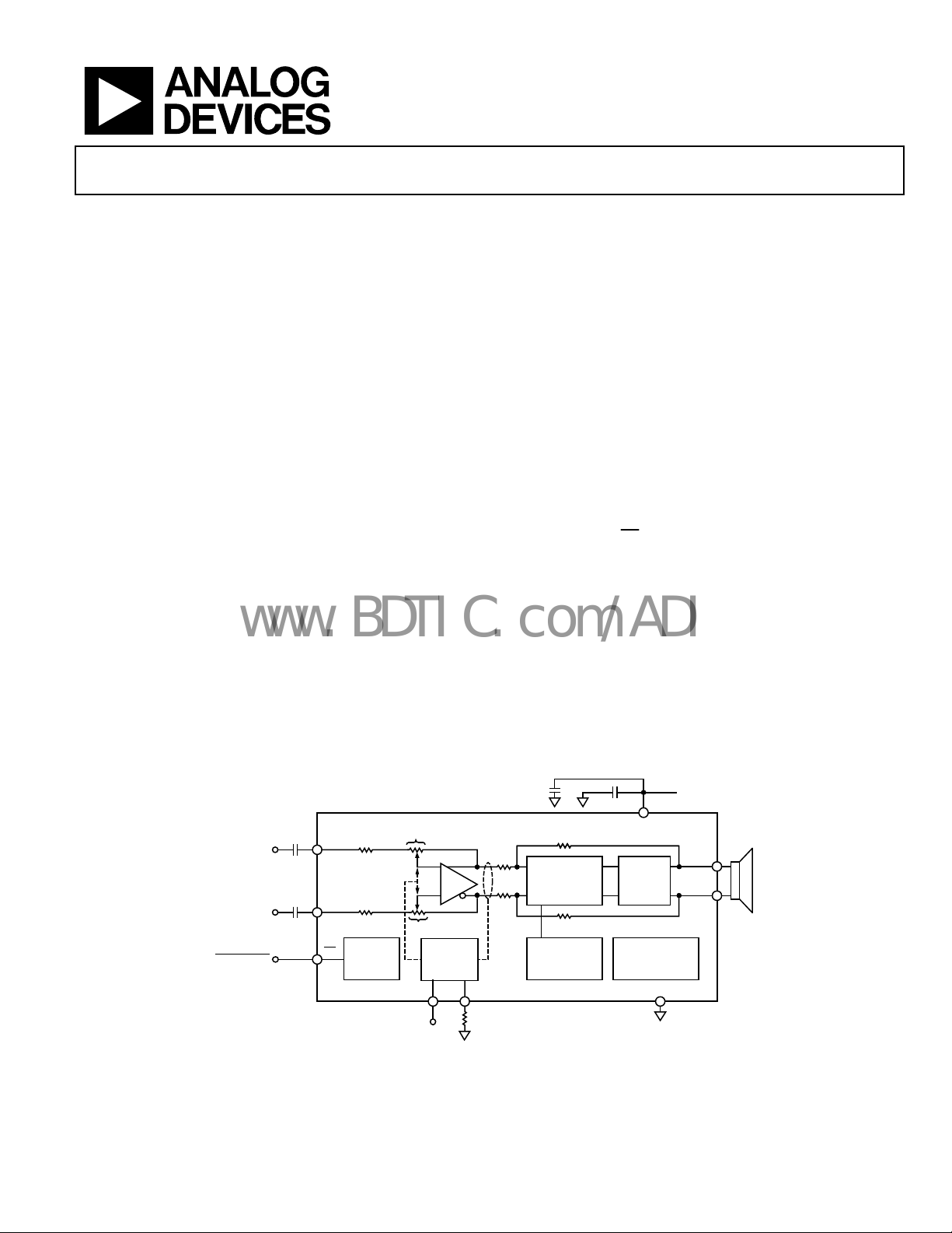
FUNCTIONAL BLOCK DIAGRAM
BIAS
80kΩ
80kΩ
ALC_EN
ALC ENABLE
/2.
DD
ALC
1
AUDIO IN+
AUDIO IN–
SHUTDOWN
Rev. A
Information furnished by Analog Devices is believed to be accurate and reliable. However, no
responsibility is assumed by Analog Devices for its use, nor for any infringements of patents or other
rights of third parties that may result from its use. Specifications subject to change without notice. No
license is granted by implication or otherwise under any patent or patent rights of Analog Devices.
Trademarks and registered trademarks are the property of their respective owners.
0.1µF
1
0.1µF
1
INPUT CAPACITORS ARE OPTIONAL IF INPUT DC COMMON-MODE
VOLTAGE IS APPROXIMATELY V
IN+
IN–
SD
10kΩ
10kΩ
VDD
FET
GND
VBATT
2.5V TO 5.5V
OUT+
OUT–
07242-001
10µF
SSM2317
MODULATOR
(Σ-Δ)
INTERNAL
OSCILLAT OR
VTH
R
TH
Figure 1.
One Technology Way, P.O. Box 9106, Norwood, MA 02062-9106, U.S.A.
Tel: 781.329.4700 www.analog.com
Fax: 781.461.3113 ©2008 Analog Devices, Inc. All rights reserved.
0.1µF
DRIVER
POP-AND-CLICK
SUPPRESSION

SSM2317
www.BDTIC.com/ADI
TABLE OF CONTENTS
Features .............................................................................................. 1
Applications ....................................................................................... 1
General Description ......................................................................... 1
Functional Block Diagram .............................................................. 1
Revision History ............................................................................... 2
Specifications ..................................................................................... 3
Absolute Maximum Ratings ............................................................ 5
Thermal Resistance ...................................................................... 5
ESD Caution .................................................................................. 5
Pin Configuration and Function Descriptions ............................. 6
Typical Performance Characteristics ............................................. 7
Typical Application Circuits .......................................................... 13
Theory of Operation ...................................................................... 14
Overview ...................................................................................... 14
Gain .............................................................................................. 14
Pop-and-Click Suppression ...................................................... 14
Output Modulation Description .............................................. 14
Layout .......................................................................................... 14
Input Capacitor Selection .......................................................... 15
Proper Power Supply Decoupling ............................................ 15
Automatic Level Control (ALC) ............................................... 15
Operating Modes ........................................................................ 15
Attack Time, Hold Time, and Release Time ........................... 15
Output Threshold ....................................................................... 16
Enable/Disabling ALC ............................................................... 16
Outline Dimensions ....................................................................... 17
Ordering Guide .......................................................................... 17
REVISION HISTORY
6/08—Rev. 0 to Rev. A
Changes to Figure 1 .......................................................................... 1
Changes to Table 2 ............................................................................ 5
Changes to Figure 17 and Figure 18 ............................................... 9
Changes to Figure 39 and Figure 40 ............................................. 13
Changes to Ordering Guide .......................................................... 17
3/08—Revision 0: Initial Version
Rev. A | Page 2 of 20
SSM2317
www.BDTIC.com/ADI
SPECIFICATIONS
VDD = 5.0 V, TA = 25°C, RL = 8 Ω + 33 µH, ALC = off, unless otherwise noted.
Table 1.
Parameter Symbol Conditions Min Typ Max Unit
DEVICE CHARACTERISTICS
Output Power PO R
R
R
R
R
R
R
R
R
R
R
R
Efficiency η PO = 1.4 W, 8 Ω, VDD = 5.0 V 93 %
Total Harmonic Distortion + Noise THD + N PO = 1 W into 8 Ω, f = 1 kHz, VDD = 5.0 V 0.02 %
P
1.0 VDD − 1.0 V
Input Common-Mode Voltage
V
CM
Range
Common-Mode Rejection Ratio CMRR
Average Switching Frequency fSW 280 kHz
Differential Output Offset Voltage V
OOS
POWER SUPPLY
Supply Voltage Range V
DD
Power Supply Rejection Ratio PSRR VDD = 2.5 V to 5.0 V, dc input floating 70 85 dB
PSRR
Supply Current (Typically, 170 μA
GSM
I
SY
Increase with ALC On)
V
V
V
V
V
Shutdown Current ISD
GAIN CONTROL
Closed-Loop Gain Gain 18 dB
Differential Input Impedance Z
IN
SHUTDOWN CONTROL
Input Voltage High V
Input Voltage Low V
Wake-Up Time t
Shutdown Time t
Output Impedance Z
WU
SD
IH
IL
OUT
= 8 Ω, THD = 1%, f = 1 kHz, 20 kHz BW, VDD = 5.0 V 1.42 W
L
= 8 Ω, THD = 1%, f = 1 kHz, 20 kHz BW, VDD = 3.6 V 0.72 W
L
= 8 Ω, THD = 10%, f = 1 kHz, 20 kHz BW, VDD = 5.0 V 1.77 W
L
= 8 Ω, THD = 10%, f = 1 kHz, 20 kHz BW, VDD = 3.6 V 0.91 W
L
= 4 Ω, THD = 1%, f = 1 kHz, 20 kHz BW, VDD = 5.0 V 2.53 W
L
= 4 Ω, THD = 1%, f = 1 kHz, 20 kHz BW, VDD = 3.6 V 1.27 W
L
= 4 Ω, THD = 10%, f = 1 kHz, 20 kHz BW, VDD = 5.0 V 3.161 W
L
= 4 Ω, THD = 10%, f = 1 kHz, 20 kHz BW, VDD = 3.6 V 1.59 W
L
= 3 Ω, THD = 1%, f = 1 kHz, 20 kHz BW, VDD = 5.0 V 3.11
L
= 3 Ω, THD = 1%, f = 1 kHz, 20 kHz BW, VDD = 3.6 V 1.55 W
L
= 3 Ω, THD = 10%, f = 1 kHz, 20 kHz BW, VDD = 5.0 V 3.89
L
= 3 Ω, THD = 10%, f = 1 kHz, 20 kHz BW, VDD = 3.6 V 1.94 W
L
= 0.5 W into 8 Ω, f = 1 kHz, VDD = 3.6 V 0.02 %
O
GSM VCM
= 2.5 V ± 100 mV at 217 Hz, output referred 57 dB
1
W
1
W
Gain = 18 dB 2.0 mV
Guaranteed from PSRR test 2.5 5.5 V
V
= 100 mV at 217 Hz, inputs ac grounded,
RIPPLE
= 0.1 μF
C
IN
60 dB
VIN = 0 V, no load, VDD = 5.0 V 3.6 mA
= 0 V, no load, VDD = 3.6 V 3.2 mA
IN
= 0 V, no load, VDD = 2.5 V 2.7 mA
IN
= 0 V, load = 8 Ω + 33 μH, VDD = 5.0 V 3.7 mA
IN
= 0 V, load = 8 Ω + 33 μH, VDD = 3.6 V 3.3 mA
IN
= 0 V, load = 8 Ω + 33 μH, VDD = 2.5 V 2.8 mA
IN
= GND
SD
SD = VDD
= GND
SD
20 nA
10 kΩ
10 kΩ
ISY ≥ 1 mA 1.2 V
ISY ≤ 300 nA 0.5 V
SD rising edge from GND to VDD
SD falling edge from VDD to GND
= GND
SD
28 ms
5 μs
>100 kΩ
Rev. A | Page 3 of 20
SSM2317
www.BDTIC.com/ADI
Parameter Symbol Conditions Min Typ Max Unit
NOISE PERFORMANCE
Output Voltage Noise en
Signal-to-Noise Ratio SNR PO = 1.4 W, RL = 8 Ω 93 dB
1
Although the SSM2317 has good audio quality above 3 W, continuous output power beyond 3 W must be avoided due to device packaging limitations.
= 3.6 V, f = 20 Hz to 20 kHz, inputs are ac grounded,
V
DD
gain = 18 dB, A-weighted
72 μV
Rev. A | Page 4 of 20
SSM2317
www.BDTIC.com/ADI
ABSOLUTE MAXIMUM RATINGS
Absolute maximum ratings apply at TA = 25°C, unless otherwise noted.
Table 2.
Parameter Rating
Supply Voltage 6 V
Input Voltage V
Common-Mode Input Voltage V
Continuous Output Power 3 W
Storage Temperature Range −65°C to +150°C
Operating Temperature Range −40°C to +85°C
Junction Temperature Range −65°C to +165°C
Lead Temperature (Soldering, 60 sec) 300°C
ESD Susceptibility 4 kV
DD
DD
THERMAL RESISTANCE
θJA is specified for the worst-case conditions, that is, a device
soldered in a circuit board for surface-mount packages.
Table 3. Thermal Resistance
Package Type PCB θJA θJB Unit
9-Ball, 1.5 mm × 1.5 mm WLCSP 1S0P 162 39 °C/W
2S0P 76 21 °C/W
ESD CAUTION
Stresses above those listed under Absolute Maximum Ratings
may cause permanent damage to the device. This is a stress
rating only; functional operation of the device at these or any
other conditions above those indicated in the operational
section of this specification is not implied. Exposure to absolute
maximum rating conditions for extended periods may affect
device reliability.
Rev. A | Page 5 of 20
SSM2317
www.BDTIC.com/ADI
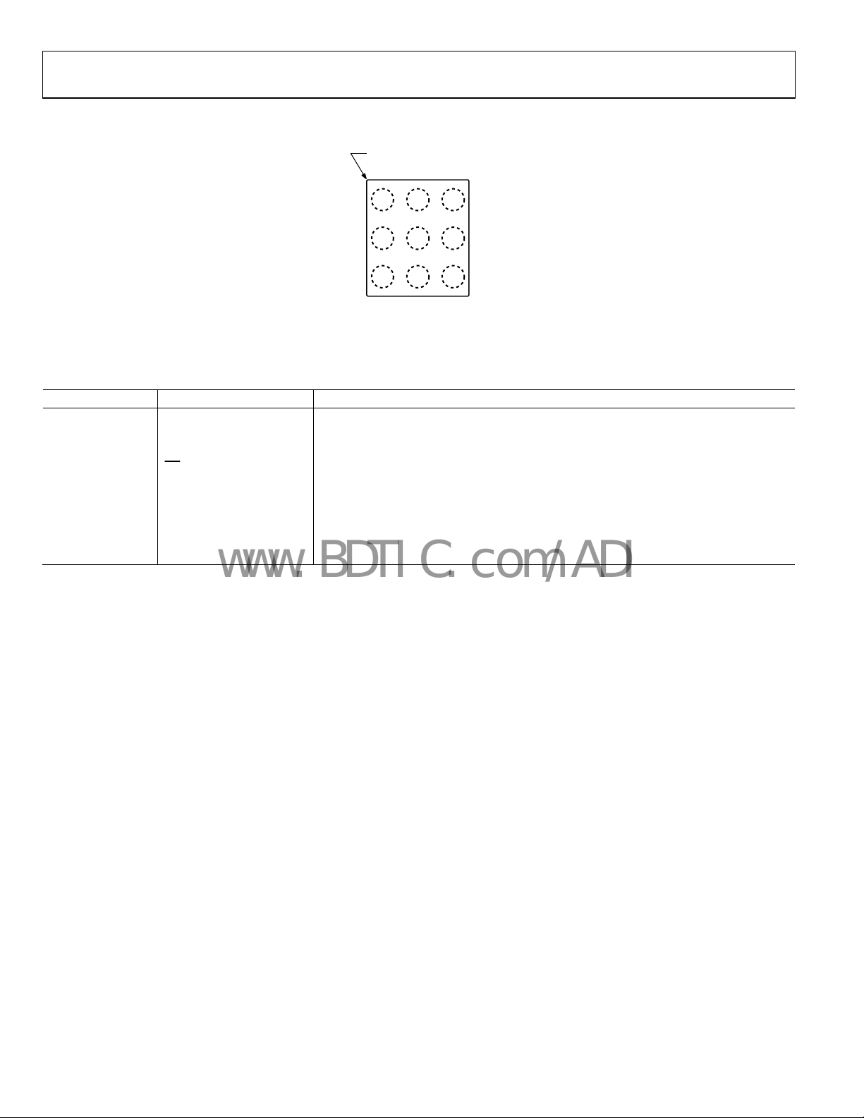
PIN CONFIGURATION AND FUNCTION DESCRIPTIONS
BALL A1
CORNER
A
B
C
SSM2317
TOP VIEW
(BALL SIDE DO WN)
Not to Scale
Figure 2. Pin Configuration
Table 4. Pin Function Descriptions
Pin No. Mnemonic Description
1A IN− Inverting Input.
1B IN+ Noninverting Input.
1C GND Ground.
2A
2B ALC_EN Automatic Level Control Enable Input. Active high digital input.
2C VDD Power Supply.
3A VTH Variable Threshold.
3B OUT− Inverting Output.
3C OUT+ Noninverting Output.
SD
Shutdown Input. Active low digital input.
321
07242-002
Rev. A | Page 6 of 20

SSM2317
www.BDTIC.com/ADI
TYPICAL PERFORMANCE CHARACTERISTICS
100
RL = 8Ω + 33µH
GAIN = 18dB
10
1
VDD = 3.6V
VDD = 2.5V
100
10
1
VDD = 5V
GAIN = 18dB
R
= 8Ω + 33µH
L
0.1
THD + N (%)
0.01
0.001
0.0001 0.001 0.01 0.1 1 10
OUTPUT PO WER (W)
VDD = 5V
07242-003
0.1
THD + N (%)
0.25W
0.01
0.001
10 100 1k 10k 100k
0.5W
1W
FREQUENCY (Hz)
07242-006
Figure 3. THD + N vs. Output Power into 8 Ω + 33 μH, Gain = 18 dB Figure 6. THD + N vs. Frequency, VDD = 5 V, RL = 8 Ω + 33 μH, Gain = 18 dB
100
RL = 4Ω + 33µH
GAIN = 18d B
10
1
0.1
THD + N (%)
0.01
0.001
0.0001 0.001 0.01 0.1 1 10
OUTPUT PO WER (W)
VDD = 3.6V
VDD = 2.5V
VDD = 5V
07242-004
100
VDD = 5V
GAIN = 18d B
R
= 4Ω + 33µH
L
10
1
0.1
THD + N (%)
0.01
0.001
10 100 1k 10k 100k
FREQUENCY (Hz)
0.5W
2W
1W
07242-007
Figure 4. THD + N vs. Output Power into 4 Ω + 33 μH, Gain = 18 dB Figure 7. THD + N vs. Frequency, VDD = 5 V, RL = 4 Ω + 33 μH, Gain = 18 dB
100
RL = 3Ω + 33µH
GAIN = 18dB
10
1
0.1
THD + N (%)
0.01
0.001
0.0001 0.001 0.01 0.1 1 10
OUTPUT POW ER (W)
VDD = 3.6V
VDD = 2.5V
VDD = 5V
07242-005
Figure 5. THD + N vs. Output Power into 3 Ω + 33 μH, Gain = 18 dB Figure 8. THD + N vs. Frequency, VDD = 5 V, RL = 3 Ω + 33 μH, Gain = 18 dB
Rev. A | Page 7 of 20
100
VDD = 5V
GAIN = 18dB
R
= 3Ω + 33µH
L
10
3W
1
0.1
THD + N (%)
0.01
0.001
10 100 1k 10k 100k
1.5W
0.75W
FREQUENCY (Hz)
07242-008

SSM2317
www.BDTIC.com/ADI
100
10
VDD = 3.6V
GAIN = 18dB
= 8Ω + 33µH
R
L
100
10
VDD = 2.5V
GAIN = 18dB
R
= 8Ω + 33µH
L
1
0.1
THD + N (%)
0.125W
0.01
0.001
10 100 1k 10k 100k
FREQUENCY (Hz)
0.5W
0.25W
07242-009
Figure 9. THD + N vs. Frequency, VDD = 3.6 V, RL = 8 Ω + 33 μH, Gain = 18 dB
100
VDD = 3.6V
GAIN = 18d B
= 4Ω + 33µH
R
L
10
1
0.1
THD + N (%)
0.01
0.001
10 100 1k 10k 100k
0.25W
1W
0.5W
FREQUENCY (Hz)
07242-010
Figure 10. THD + N vs. Frequency, VDD = 3.6 V, RL = 4 Ω + 33 μH, Gain = 18 dB
1
0.1
THD + N (%)
0.01
0.0625W
0.001
10 100 1k 10k 100k
0.25W
0.125W
FREQUENCY (Hz)
07242-012
Figure 12. THD + N vs. Frequency, VDD = 2.5 V, RL = 8 Ω + 33 μH, Gain = 18 dB
100
VDD = 2.5V
GAIN = 18d B
R
= 4Ω + 33µH
L
10
1
0.1
THD + N (%)
0.01
0.001
10 100 1k 10k 100k
0.5W
0.125W
0.25W
FREQUENCY (Hz)
07242-013
Figure 13. THD + N vs. Frequency, VDD = 2.5 V, RL = 4 Ω + 33 μH, Gain = 18 dB
100
VDD = 3.6V
GAIN = 18dB
R
= 3Ω + 33µH
L
10
1.5W
1
0.1
THD + N (%)
0.75W
0.01
0.38W
0.001
10 100 1k 10k 100k
FREQUENCY (Hz)
07242-011
Figure 11. THD + N vs. Frequency, VDD = 3.6 V, RL = 3 Ω + 33 μH, Gain = 18 dB
Rev. A | Page 8 of 20
100
VDD = 2.5V
GAIN = 18d B
R
= 3Ω + 33µH
L
10
1
0.1
THD + N (%)
0.01
0.001
10 100 1k 10k 100k
0.75W
0.375W
0.188W
FREQUENCY (Hz)
07242-014
Figure 14. THD + N vs. Frequency, VDD = 2.5 V, RL = 3 Ω + 33 μH, Gain = 18 dB

SSM2317
www.BDTIC.com/ADI
4.4
4.2
4.0
3.8
3.6
3.4
3.2
SUPPLY CURRENT (mA)
3.0
2.8
2.6
2.5 3.0 3.5 4.0 4.5 5.0 5.5 6.0
RL = 4Ω + 33µH
SUPPLY VOLTAGE (V)
RL = 8Ω + 33µH
NO LOAD
Figure 15. Supply Current vs. Supply Voltage
07242-015
4.5
FREQUENCY = 1kHz
GAIN = 18dB
4.0
R
= 3Ω + 33µH
L
3.5
3.0
2.5
2.0
1.5
OUTPUT PO WER (W)
1.0
0.5
0
2.5 3.0 3.5 4.0 4.5 5.0
DO NOT EXCE ED 3W
CONTINUO US OUTPUT POWER
10%
1%
SUPPLY VOLTAGE (V)
Figu re 18. Maximum Output Power vs. Supply Voltage,
= 3 Ω + 33 μH, Gain = 18 dB
R
L
07242-018
2.0
FREQUENCY = 1kHz
GAIN = 18dB
1.8
R
= 8Ω + 33µH
L
1.6
1.4
1.2
1.0
0.8
0.6
OUTPUT POWER (W)
0.4
0.2
0
2.5 3.0 3.5 4.0 4.5 5.0
10%
1%
SUPPLY VOLTAGE (V)
Figu re 16. Maximum Output Power vs. Supply Voltage,
= 8 Ω + 33 μH, Gain = 18 dB
R
L
3.5
3.0
FREQUENCY = 1kHz
GAIN = 18dB
2.5
R
= 4Ω + 33µH
L
2.0
1.5
OUTPUT POW ER (W)
1.0
0.5
0
2.5 3.0 3.5 4.0 4.5 5.0
DO NOT EXCE ED 3W
CONTINUO US OUTPUT POWER
10%
1%
SUPPLY VOLTAGE (V)
Figu re 17. Maximum Output Power vs. Supply Voltage,
= 4 Ω + 33 μH, Gain = 18 dB
R
L
100
VDD = 2.5V
90
80
70
VDD = 3.6V
60
50
40
EFFICIENCY (%)
30
20
10
0
0 0.2 0.4 0.6 0.8 1.0 1.2 1.4 1.6
07242-016
VDD = 5V
OUTPUT POWER (W)
RL = 8Ω + 33µH
07242-019
Figure 19. Efficiency vs. Output Power into 8 Ω + 33 μH
100
90
80
VDD = 2.5V
70
60
50
40
EFFICIENCY (%)
30
20
10
0
0 0.2 0.4 0.6 0. 8 1.0 1. 2 1.4 1.6 1.8 2.0 2. 2 2.4 2.6 2.8 3.0 3. 2
07242-017
VDD = 3.6V
OUTPUT PO WER (W)
RL = 4Ω + 33µH
VDD = 5V
07242-020
Figure 20. Efficiency vs. Output Power into 4 Ω + 33 μH
Rev. A | Page 9 of 20

SSM2317
www.BDTIC.com/ADI
100
90
80
70
60
50
40
EFFICIENCY (%)
30
20
10
VDD = 2.5V
0
0 0.2 0.4 0.6 0.8 1.0 1.2 1.4 1.6 1.8 2.0 2.2 2.4 2.6 2.8 3.0 3.2
VDD = 3.6V
OUTPUT PO WER (W)
RL = 3Ω + 33µH
VDD = 5V
Figure 21. Efficiency vs. Output Power into 3 Ω + 33 μH
07242-021
0.6
RL = 3Ω + 33µH
0.5
0.4
0.3
VDD = 2.5V
0.2
POWER DISSIPATION ( W)
0.1
0
0 0.2 0.4 0.6 0.8 1.0 1.2 1.4 1.6 1.8 2.0 2.2 2.4 2.6 2.8 3.0 3.2
VDD = 3.6V
OUTPUT PO WER (W)
VDD = 5V
Figure 24. Power Dissipation vs. Output Power into 3 Ω + 33 μH
07242-024
0.12
RL = 8Ω + 33µH
0.10
0.08
0.06
0.04
POWER DISSIPATION (W)
0.02
VDD = 2.5V
0
0 0.2 0.4 0.6 0.8 1.0 1.2 1.4 1.6
VDD = 3.6V
OUTPUT PO WER (W)
VDD = 5V
Figure 22. Power Dissipation vs. Output Power into 8 Ω + 33 μH
0.45
RL = 4Ω + 33µH
0.40
0.35
0.30
0.25
0.20
VDD = 2.5V
0.15
POWE R DISSI PATION (W)
0.10
0.05
0
0 0.2 0.4 0.6 0.8 1.0 1. 2 1. 4 1. 6 1. 8 2. 0 2.2 2. 4 2.6 2. 8 3. 0 3. 2
VDD = 3.6V
OUTPUT PO WER (W)
VDD = 5V
Figure 23. Power Dissipation vs. Output Power into 4 Ω + 33 μH
350
RL = 8Ω + 33µH
300
250
200
150
100
SUPPLY CURRENT (mA)
50
0
0 0.2 0.4 0.6 0.8 1.0 1.2 1.4 1.6
07242-022
VDD = 2.5V
VDD = 3.6V
OUTPUT POWER (W)
VDD = 5V
07242-025
Figure 25. Supply Current vs. Output Power into 8 Ω + 33 μH
800
RL = 4Ω + 33µH
700
600
500
400
300
SUPPLY CURRENT (mA)
200
100
0
07242-023
VDD = 2.5V
0 0.2 0.4 0.6 0.8 1.0 1.2 1.4 1.6 1.8 2.0 2.2 2.4 2.6 2.8 3.0 3.2
VDD = 3.6V
OUTPUT PO WER (W)
VDD = 5V
07242-026
Figure 26. Supply Current vs. Output Power into 4 Ω + 33 μH
Rev. A | Page 10 of 20

SSM2317
www.BDTIC.com/ADI
1000
RL = 3Ω + 33µH
900
800
700
600
500
400
300
SUPPLY CURRENT (mA)
200
100
0
0 0.2 0.4 0.6 0.8 1.0 1.2 1.4 1.6 1.8 2.0 2.2 2.4 2.6 2.8 3.0 3.2
VDD = 2.5V
OUTPUT PO WER (W)
VDD = 3.6V
VDD = 5V
Figure 27. Supply Current vs. Output Power into 3 Ω + 33 μH
07242-027
4.4
4.2
4.0
3.8
3.6
3.4
3.2
SUPPLY CURRENT (mA)
3.0
2.8
2.6
2.5 3.0 3.5 4.0 4.5 5.0 5.5 6.0
ALC = ON
NO LOAD
ALC = OFF
NO LOAD
SUPPLY VOLTAGE (V)
Figure 30. Supply Current vs. Supply Voltage, ALC Contribution
07242-030
0
–10
–20
–30
–40
–50
PSRR (dB)
–60
–70
–80
–90
–100
10 1 00 1k 10k 100k
FREQUENCY (Hz)
Figure 28. Power Supply Rejection Ratio vs. Frequency
0
–10
–20
–30
–40
–50
–60
CMRR (dB)
–70
–80
–90
–100
10 100 1k 10k 100k
FREQUENCY (Hz)
Figure 29. Common-Mode Rejection Ratio vs. Frequency
100
90
80
(%)
70
TH
V
60
50
40
0.1 10 1k 100k1 100 10k
07242-028
R
(kΩ)
TH
07242-031
Figure 31. VTH vs. RTH
10
VDD = 5V
R
= 8Ω + 33µH
L
ALC = ON
1
0.1
OUTPUT POW ER (W)
0.01
0.001
0.01 0. 1 1 10
07242-029
INPUT (V rms)
VTH = 90%
VTH = 70%
VTH = 45%
07242-032
Figure 32. Input/Output Characteristic, VDD = 5 V, ALC = On
Rev. A | Page 11 of 20

SSM2317
–
www.BDTIC.com/ADI
OUTPUT POW ER (W)
0.1
0.01
10
1
VDD = 3.6V
R
= 8Ω + 33µH
L
ALC = ON
VTH = 90%
VTH = 70%
VTH = 45%
1V/DIV
INPUT
HOLD TIM E
RELEASE TI ME
OUTPUT
VDD = 5V
R
= 8Ω + 33µH
L
ALC = ON
V
= 70%
TH
0.001
0.01 0. 1 1 10
Figure 33. Input/Output Characteristic, V
1V/DIV
INPUT
OUTPUT
–0.2 0 0.2 0.4 0. 6 0. 8 1.0 1.2 1.4 1.6 1. 8
INPUT (V rms)
TIME (ms)
= 3.6 V, ALC = On
DD
VDD = 5V
R
= 8Ω + 33µH
L
ALC = ON
V
= 70%
TH
Figure 34. Attack Waveform, 1 kHz Sine Wave
1V/DIV
100 0 100 200 300 400 500 600 700 800 900
07242-033
TIME (ms)
07242-036
Figure 36. Release Waveform
6
1V/DIV
5
4
3
2
VOLTAGE (V)
1
0
–1
07242-034
–4 0 4 8 12162024283236
SD INPUT
OUTPUT
TIME (ms)
07242-037
Figure 37. Turn-On Response
6
SD INPUT
5
1V/DIV
INPUT
ATTACK TIME
OUTPUT
–0.1 0 0.1 0.2 0.3 0.4 0.5 0.6 0.7 0.8 0.9
TIME (ms)
VDD = 5V
R
= 8Ω + 33µH
L
ALC = ON
V
= 70%
TH
07242-035
Rev. A | Page 12 of 20
4
3
2
VOLTAGE (V)
1
0
–1
–120 –80 –40 0 40 80 120 160 200 240 280
OUTPUT
TIME (µs)
Figure 38. Turn-Off Response Figure 35. Attack Waveform, 3 kHz Sine Wave
07242-038

SSM2317
www.BDTIC.com/ADI
TYPICAL APPLICATION CIRCUITS
EXTERNAL GAIN SETTINGS = 80kΩ/(10kΩ + R
1
0.1µF
R
AUDIO IN+
AUDIO IN–
SHUTDOWN
0.1µF
EXT
1
R
EXT
10kΩ
IN+
10kΩ
IN–
SD
BIAS
1
INPUT CAPACITO RS ARE OPTI ONAL IF INPUT DC COMM ON-MODE
VOLTAGE IS APPROXI MATELY V
Figure 39. Differential Input Configuration, User-Adjustable Gain
EXTERNAL GAIN SETTINGS = 80kΩ/(10kΩ + R
0.1µF
R
AUDIO IN+
SHUTDOWN
0.1µF
EXT
R
EXT
IN+
IN–
SD
10kΩ
10kΩ
BIAS
Figure 40. Single-Ended Input Configuration, User-Adjustable Gain
)
EXT
80kΩ
80kΩ
ALC_EN
ALC ENABLE
)
EXT
80kΩ
80kΩ
ALC_EN
ALC ENABLE
ALC
ALC
VTH
R
DD
VTH
R
TH
/2.
TH
10µF
SSM2317
MODULATOR
INTERNAL
OSCILLATOR
10µF
SSM2317
MODULATOR
INTERNAL
OSCILLATOR
(Σ-Δ)
(Σ-Δ)
0.1µF
VDD
FET
DRIVER
POP-AND-CLICK
SUPPRESSION
0.1µF
VDD
FET
DRIVER
POP-AND-CLICK
SUPPRESSION
GND
GND
VBATT
2.5V TO 5.5V
OUT+
OUT–
VBATT
2.5V TO 5.5V
OUT+
OUT–
07242-039
07242-040
Rev. A | Page 13 of 20

SSM2317
www.BDTIC.com/ADI
THEORY OF OPERATION
OVERVIEW
The SSM2317 mono Class-D audio amplifier features a filterless
modulation scheme that greatly reduces the external components
count, conserving board space and, thus, reducing systems cost.
The SSM2317 does not require an output filter but instead relies
on the inherent inductance of the speaker coil and the natural
filtering of the speaker and human ear to fully recover the audio
component of the square wave output. Most Class-D amplifiers
use some variation of pulse-width modulation (PWM), but the
SSM2317 uses a Σ- modulation to determine the switching
pattern of the output devices, resulting in a number of important benefits. Σ- modulators do not produce a sharp peak with
many harmonics in the AM frequency band, as pulse-width
modulators often do. Σ- modulation provides the benefits of
reducing the amplitude of spectral components at high frequencies,
that is, reducing EMI emission that might otherwise be radiated
by speakers and long cable traces. Due to the inherent spread
spectrum nature of Σ- modulation, the need for oscillator
synchronization is eliminated for designs incorporating multiple
SSM2317 amplifiers.
The SSM2317 also offers protection circuits for overcurrent and
temperature protection.
GAIN
The SSM2317 has a default gain of 18 dB that can be reduced by
using a pair of external resistors with a value calculated as follows:
External Gain Settings = 80 kΩ/(10 kΩ + R
EXT
)
POP-AND-CLICK SUPPRESSION
Voltage transients at the output of the audio amplifiers can
occur when shutdown is activated or deactivated. Voltage
transients as low as 10 mV can be heard as an audio pop in the
speaker. Clicks and pops can also be classified as undesirable
audible transients generated by the amplifier system and,
therefore, as not coming from the system input signal. Such
transients can be generated when the amplifier system changes its
operating mode. For example, the following can be sources of
audible transients: system power-up/power-down, mute/unmute,
input source change, and sample rate change. The SSM2317 has a
pop-and-click suppression architecture that reduces these
output transients, resulting in noiseless activation and
deactivation.
OUTPUT MODULATION DESCRIPTION
The SSM2317 uses three-level, Σ- output modulation. Each
output can swing from GND to VDD and vice versa. Ideally,
when no input signal is present, the output differential voltage is
0 V because there is no need to generate a pulse. In a real-world
situation, there are always noise sources present. Due to this
constant presence of noise, a differential pulse is generated,
when required, in response to this stimulus. A small amount of
current flows into the inductive load when the differential pulse
is generated.
Rev. A | Page 14 of 20
However, most of the time, output differential voltage is 0 V,
due to the Analog Devices, Inc., patented three-level, Σ-
output modulation. This feature ensures that the current
flowing through the inductive load is small.
When the user wants to send an input signal, an output pulse
is generated to follow the input voltage. The differential pulse
density is increased by raising the input signal level. Figure 41
depicts three-level, Σ- output modulation with and without
input stimulus.
OUTPUT = 0V
OUT+
OUT–
V
OUT
OUTPUT > 0V
OUT+
OUT–
V
OUT
OUTPUT < 0V
OUT+
OUT–
V
OUT
Figu re 41. Three-L evel, Σ-Δ Output Modulation With and Without Input Stimulus
+5V
0V
+5V
0V
+5V
0V
–5V
+5V
0V
+5V
0V
+5V
0V
+5V
0V
+5V
0V
0V
–5V
07242-041
LAYOUT
As output power continues to increase, care must be taken
to lay out PCB traces and wires properly among the amplifier,
load, and power supply. A good practice is to use short, wide
PCB tracks to decrease voltage drops and minimize inductance.
Ensure that track widths are at least 200 mil for every inch of
track length for lowest DCR, and use 1 oz or 2 oz of copper PCB
traces to further reduce IR drops and inductance. A poor layout
increases voltage drops, consequently affecting efficiency. Use
large traces for the power supply inputs and amplifier outputs
to minimize losses due to parasitic trace resistance.
Proper grounding guidelines help improve audio performance,
minimize crosstalk between channels, and prevent switching
noise from coupling into the audio signal. To maintain high
output swing and high peak output power, the PCB traces that
connect the output pins to the load and supply pins should be as
wide as possible to maintain the minimum trace resistances. It
is also recommended that a large ground plane be used for
minimum impedances.
In addition, good PCB layouts isolate critical analog paths from
sources of high interference. Separate high frequency circuits
(analog and digital) from low frequency circuits.
Properly designed multilayer PCBs can reduce EMI emission
and increase immunity to the RF field by a factor of 10 or more,

SSM2317
www.BDTIC.com/ADI
compared with double-sided boards. A multilayer board allows
a complete layer to be used for the ground plane, whereas the
ground plane side of a double-sided board is often disrupted with
signal crossover.
If the system has separate analog and digital ground and power
planes, place the analog ground plane underneath the analog power
plane, and, similarly, place the digital ground plane underneath the
digital power plane. There should be no overlap between analog
and digital ground planes or analog and digital power planes.
INPUT CAPACITOR SELECTION
The SSM2317 does not require input coupling capacitors if
the input signal is biased from 1.0 V to V
− 1.0 V. Input
DD
capacitors are required if the input signal is not biased within
this recommended input dc common-mode voltage range, if
high-pass filtering is needed, or if a single-ended source is used.
If high-pass filtering is needed at the input, the input capacitor
and the input resistor of the SSM2317 form a high-pass filter
whose corner frequency is determined by the following
equation:
f
= 1/{2π × (10 kΩ + R
C
) × CIN}
EXT
The input capacitor can significantly affect the performance of
the circuit. Not using input capacitors degrades both the output
offset of the amplifier and the dc PSRR performance.
PROPER POWER SUPPLY DECOUPLING
To ensure high efficiency, low total harmonic distortion (THD),
and high PSRR, proper power supply decoupling is necessary.
Noise transients on the power supply lines are short-duration
voltage spikes. Although the actual switching frequency can
range from 10 kHz to 100 kHz, these spikes can contain frequency
components that extend into the hundreds of megahertz. The
power supply input needs to be decoupled with a good quality
low ESL, low ESR capacitor, usually of around 4.7 µF. This
capacitor bypasses low frequency noises to the ground plane.
For high frequency transient noises, use a 0.1 µF capacitor as
close as possible to the VDD pin of the device. Placing the
decoupling capacitor as close as possible to the SSM2317 helps
maintain efficient performance.
AUTOMATIC LEVEL CONTROL (ALC)
Automatic level control (ALC) is a function that automatically
adjusts amplifier gain to generate desired output amplitude with
reference to a particular input stimulus. The primary motivation
for the use of ALC is to protect an audio power amplifier or
speaker load from the damaging effects of clipping or current
overloading. This is accomplished by limiting the amplifier’s
output amplitude upon reaching a preset threshold voltage. A
less intuitive benefit of ALC is that it makes sound sources with
a wide dynamic range more intelligible by boosting low level
signals yet limits very high level signals.
Figure 42 shows input vs. output and gain characteristics of
ALC that is implemented in the SSM2317.
24
21
18
15
12
GAIN (dB)
9
6
3
0
–30 –20 –10 0 10
GAIN
INPUT (dBV)
Figure 42. Input/Output Characteristic and Gain
OUTPUT
12
9
6
3
0
–3
OUTPUT (dBV)
–6
–9
–12
07242-042
When the input level is small and below the ALC threshold
value, the gain of the amplifier stays at 18 dB. When the input
exceeds the ALC threshold value, the ALC begins to gradually
reduce the gain from 18 dB to 3.5 dB.
OPERATING MODES
The ALC implemented on SSM2317 has two operating modes:
compression and limiting. At the time the ALC is triggered for
medium level input, the ALC is in compression mode. In this
mode, an increase of the output signal is 1/3 of the increase of
the input signal. For example, if the input signal increases by
3 dB, the ALC reduces the amplifier gain by 2 dB and thus the
output signal only increases by 1 dB.
As the input signal becomes very large, the ALC transitions into
limiting operation mode. In this mode, the output stays at a
given threshold level, V
, even if the input signal grows larger.
TH
For example, when a large input signal increases by 3 dB, the
ALC reduces the amplifier gain by 3 dB and thus the output
increases 0 dB. When the amplifier gain is reduced to 3.5 dB,
ALC cannot further reduce the gain and the output increases
again. To avoid potential speaker damage, the maximum input
signal should not be large enough to exceed the maximum
attenuation (3.5 dB) of the limiting operational mode.
ATTACK TIME, HOLD TIME, AND RELEASE TIME
When the amplifier input exceeds a preset threshold, ALC
reduces amplifier gain rapidly until its output settles to a target
level. This gain level is maintained for a certain period. If the
input does not exceed the threshold again, ALC increases the
gain gradually. The attack time is the time taken to reduce the
gain from maximum to minimum. The hold time is the time to
sustain the reduced gain. The release time is the time taken to
increase the gain from minimum to maximum. These times are
shown in Tab l e 5.
Table 5. Attack, Hold, and Release Times
Time Duration (ms)
Attack Time 0.1
Hold Time 35
Release Time 550
Rev. A | Page 15 of 20

SSM2317
www.BDTIC.com/ADI
OUTPUT THRESHOLD
The maximum output amplitude threshold (VTH) during the
limiting mode can be changed from 90% to 45% of V
having an external resistor, R
Shorting the VTH pin to GND sets V
the VTH pin unconnected sets V
of R
to VTH is shown by the following equation:
TH
V ×
TH
9.0
k50
×=
Maximum output power is derived from V
, between the VTH pin and GND.
TH
to 90% of VDD. Leaving
TH
to 45% of VDD. The relation
TH
R
+
TH
R
×+
2k50
TH
V
DD
by the following
TH
equation:
2
V
⎞
⎛
TH
⎟
⎜
2
⎠
⎝
=
P
OUT
where R
Figure 43 shows the relationship between the R
V
. Figure 44 shows the relationship between the maximum
TH
output power and the R
100
)
DD
R
SP
is the speaker impedance.
SP
value.
TH
90
80
TH
by
DD
value and
1400
1200
1000
800
600
400
OUTPUT PO WER (mW)
200
0
0.1 1 10 100 1k 10k
Figure 44. Maximum Output Power vs. R
4.2V (8Ω)
3.6V (8Ω)
2.5V (8Ω)
5V (8Ω)
(kΩ)
R
TH
TH
07242-044
ENABLE/DISABLING ALC
The ALC function is enabled when the ALC_EN pin is set to
V
. The ACL function can be enabled and disabled during
DD
amplifier operation. As a result of enabling ALC, I
by 100 µA and there is less than 50 µA source current from the
VTH pin to GND via R
. When ALC is disabled, the source
TH
current is 0 µA and the VTH pin is tied to GND.
increases
SY
70
60
OUTPUT SWING (% of V
50
40
0.1 1 10 100 1k 10k
Figure 43. Output Threshold (V
R
(kΩ)
TH
) vs. R
TH
TH
07242-043
Rev. A | Page 16 of 20

SSM2317
www.BDTIC.com/ADI
OUTLINE DIMENSIONS
0.655
0.600
0.545
SEATING
PLANE
0.350
0.320
0.290
123
A
B
A1 BALL
CORNER
1.490
1.460 SQ
1.430
C
101507-C
TOP VIEW
(BALL SI DE DOWN)
0.385
0.360
0.335
0.50
BALL PI TCH
0.270
0.240
0.210
BOTTOM VIEW
(BALL SIDE UP)
Figure 45. 9-Ball Wafer Level Chip Scale Package [WLCSP]
(CB-9-2)
Dimensions shown in millimeters
ORDERING GUIDE
Model Temperature Range Package Description Package Option Branding
SSM2317CBZ-REEL
SSM2317CBZ-REEL7
SSM2317-EVALZ
SSM2317-MINI-EVALZ
1
Z = RoHS Compliant Part.
1
−40°C to +85°C 9-Ball Wafer Level Chip Scale Package [WLCSP] CB-9-2 Y0Z
1
−40°C to +85°C 9-Ball Wafer Level Chip Scale Package [WLCSP] CB-9-2 Y0Z
1
Evaluation Board
1
Evaluation Board
Rev. A | Page 17 of 20

SSM2317
www.BDTIC.com/ADI
NOTES
Rev. A | Page 18 of 20

SSM2317
www.BDTIC.com/ADI
NOTES
Rev. A | Page 19 of 20

SSM2317
www.BDTIC.com/ADI
NOTES
©2008 Analog Devices, Inc. All rights reserved. Trademarks and
registered trademarks are the property of their respective owners.
D07242-0-6/08(A)
Rev. A | Page 20 of 20
 Loading...