

2 W, Filterless, Class-D
www.BDTIC.com/ADI
FEATURES
Filterless Class-D amplifier with built-in output stage
2 W into 4 Ω and 1.4 W into 8 Ω at 5.0 V supply
Ultralow idle current with load resistance
>87% efficiency at 5.0 V, 1.4 W into 8 Ω speaker
Better than 96 dB SNR (signal-to-noise ratio)
Available in 16-lead, 3 mm × 3 mm LFCSP
Single-supply operation from 2.5 V to 5.0 V
20 nA ultralow shutdown c
Short-circuit and thermal protection
Pop-and-click suppression
Built-in resistors reduce board component count
Default fixed 18 dB gain and user-adjustable
APPLICATIONS
Mobile phones
MP3 players
Portable gaming
Portable electronics
Educational toys
Notebook computers
GENERAL DESCRIPTION
The SSM2306 is a fully integrated, high efficiency, Class-D stereo
audio amplifier designed to maximize performance for portable
applications. The application circuit requires minimum external
components and operates from a single 2.5 V to 5.0 V supply. It
is capable of delivering 2 W of continuous output power with less
than 10% THD + N driving a 4 Ω load from a 5.0 V supply.
urrent
Stereo Audio Amplifier
SSM2306
The SSM2306 features ultralow idle current, high efficiency, and
w noise modulation scheme. It operates with >87% efficiency
a lo
at 1.4 W into 8 Ω from a 5.0 V supply and has a signal-to-noise
ratio (SNR) that is better than 96 dB. PDM modulation offers lower
EMI radiated emissions compared to other Class-D architectures.
The SSM2306 has a micropower shutdown mode with a typical
utdown current of 20 nA. Shutdown is enabled by applying a
sh
logic low to the
The architecture of the device allows it to achieve a very low level
f pop and click to minimize voltage glitches at the output
o
during turn-on and turn-off, thereby reducing audible noise on
activation and deactivation. The fully differential input of the
SSM2306 provides excellent rejection of common-mode noise
on the input. Input coupling capacitors can be omitted if the dc
input common-mode voltage is approximately V
The SSM2306 also has excellent rejection of power supply noise,
cluding noise caused by GSM transmission bursts and RF
in
rectification.
The SSM2306 has a preset gain of 18 dB that can be reduced by
g external resistors.
usin
The SSM2306 is specified over the commercial temperature range
(−40°C t
short-circuit protection. It is available in a 16-lead, 3 mm × 3 mm
lead frame chip scale package (LFCSP).
SD
pin.
/2.
DD
o +85°C). It has built-in thermal shutdown and output
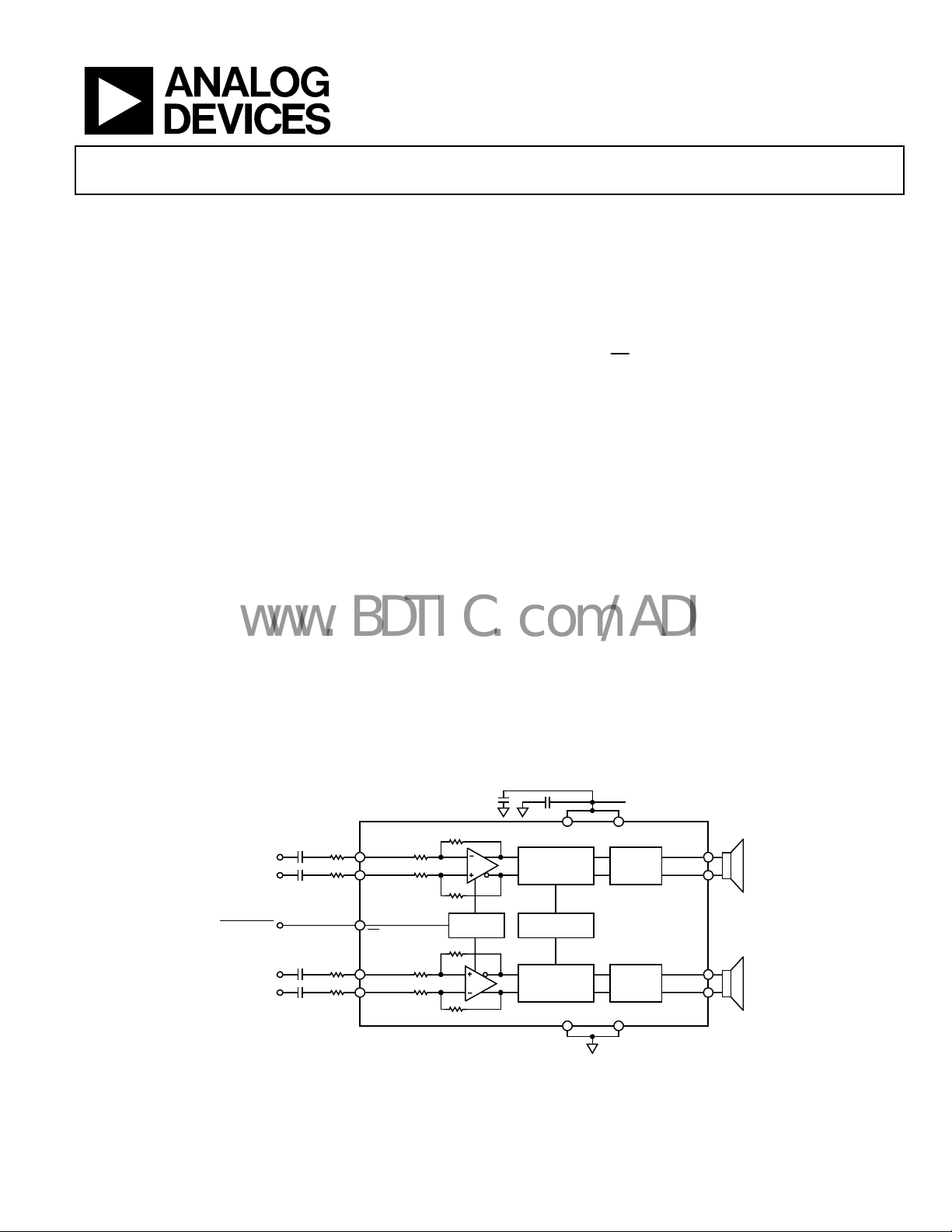
FUNCTIONAL BLOCK DIAGRAM
1
RIGHT IN+
RIGHT IN–
SHUTDOWN
LEFT IN+
LEFT IN–
GAIN = 344kΩ/(43kΩ + R
1
INPUT CAPS ARE O PTIONAL IF INPUT DC COMMON-MO DE
VOLTAGE IS APPROXIMATELY V
Rev. 0
Information furnished by Analog Devices is believed to be accurate and reliable. However, no
responsibility is assumed by Anal og Devices for its use, nor for any infringements of patents or ot her
rights of third parties that may result from its use. Specifications subject to change without notice. No
license is granted by implication or otherwise under any patent or patent rights of Analog Devices.
Trademarks and registered trademarks are the property of their respective owners.
22nF
22nF
22nF
22nF
1
1
1
SSM2306
R
EXT
INR+
INR–
R
EXT
SD
R
EXT
INL+
INL–
R
EXT
)
EXT
/2.
DD
344kΩ
43kΩ
43kΩ
344kΩ
344kΩ
43kΩ
43kΩ
344kΩ
10µF
BIAS
Figure 1.
VBATT
0.1µF
MODULATOR
INTERNAL
OSCIL LATO R
MODULATOR
One Technology Way, P.O. Box 9106, Norwood, MA 02062-9106, U.S.A.
Tel: 781.329.4700 www.analog.com
Fax: 781.461.3113 ©2007 Analog Devices, Inc. All rights reserved.
2.5V TO 5. 0V
VDDVDD
FET
DRIVER
FET
DRIVER
GNDGND
OUTR+
OUTR–
OUTL+
OUTL–
6542-001

SSM2306
www.BDTIC.com/ADI
TABLE OF CONTENTS
Features .............................................................................................. 1
Typical Applicat i o n C i rc uits ......................................................... 11
Applications....................................................................................... 1
General Description......................................................................... 1
Functional Block Diagram .............................................................. 1
Revision History ............................................................................... 2
Specifications..................................................................................... 3
Absolute Maximum Ratings............................................................ 4
Thermal Resistance ...................................................................... 4
ESD Caution.................................................................................. 4
Pin Configuration and Function Descriptions............................. 5
Typical Performance Characteristics ............................................. 6
REVISION HISTORY
4/07—Revision 0: Initial Version
Application Notes........................................................................... 12
Overview ..................................................................................... 12
Gain Selection............................................................................. 12
Pop-and-Click Suppression ...................................................... 12
EMI Noise.................................................................................... 12
Layout .......................................................................................... 13
Input Capacitor Selection.......................................................... 13
Proper Power Supply Decoupling ............................................ 13
Outline Dimensions ....................................................................... 14
Ordering Guide .......................................................................... 14
Rev. 0 | Page 2 of 16
SSM2306
www.BDTIC.com/ADI
SPECIFICATIONS
VDD = 5.0 V; TA = 25oC; RL = 4 Ω, 8 Ω; gain = 6 dB, unless otherwise noted.
Table 1.
Parameter Symbol Conditions Min Typ Max Unit
DEVICE CHARACTERISTICS
Output Power P
O
R
R
R
R
R
R
R
R
R
R
R
Efficiency η P
P
Total Harmonic Distortion + Noise THD + N PO = 2 W into 4 Ω each channel, f = 1 kHz, VDD = 5.0 V 0.4 %
P
Input Common-Mode Voltage Range V
CM
Common-Mode Rejection Ratio CMRR
Channel Separation X
Average Switching Frequency f
Differential Output Offset Voltage V
TAL K
SW
OOS
POWER SUPPLY
Supply Voltage Range V
DD
Power Supply Rejection Ratio PSRR VDD = 2.5 V to 5.0 V 70 85 dB
PSRR
Supply Current I
SY
V
V
Shutdown Current I
SD
GAIN
Closed-Loop Gain A
Differential Input Impedance Z
v
IN
SHUTDOWN CONTROL
Input Voltage High V
Input Voltage Low V
Turn-On Time t
Turn-Off Time t
Output Impedance O
IH
IL
WU
SD
UT
NOISE PERFORMANCE
Output Voltage Noise e
n
Signal-to-Noise Ratio SNR P
RL = 4 Ω, THD = 1%, f = 1 kHz, 20 kHz BW, VDD = 5.0 V 1.8 W
= 8 Ω, THD = 1%, f = 1 kHz, 20 kHz BW, VDD = 5.0 V 1.4 W
L
= 4 Ω, THD = 1%, f = 1 kHz, 20 kHz BW, VDD = 3.6 V 0.9 W
L
= 8 Ω, THD = 1%, f = 1 kHz, 20 kHz BW, VDD = 3.6 V 0.615 W
L
= 4 Ω, THD = 1%, f = 1 kHz, 20 kHz BW, VDD = 2.5 V 0.35 W
L
= 8 Ω, THD = 1%, f = 1 kHz, 20 kHz BW, VDD = 2.5 V 0.275 W
L
= 4 Ω, THD = 10%, f = 1 kHz, 20 kHz BW, VDD = 5.0 V 2.4 W
L
= 8 Ω, THD = 10%, f = 1 kHz, 20 kHz BW, VDD = 5.0 V 1.53 W
L
= 4 Ω, THD = 10%, f = 1 kHz, 20 kHz BW, VDD = 3.6 V 1.1 W
L
= 8 Ω, THD = 10%, f = 1 kHz, 20 kHz BW, VDD = 3.6 V 0.77 W
L
= 4 Ω, THD = 10%, f = 1 kHz, 20 kHz BW, VDD = 2.5 V 0.45 W
L
= 8 Ω, THD = 10%, f = 1 kHz, 20 kHz BW, VDD = 2.5 V 0.35 W
L
= 2 W, 4 Ω, VDD = 5.0 V 75 %
OUT
= 1.4 W, 8 Ω, VDD = 5.0 V 85 %
OUT
= 1 W into 8 Ω each channel, f = 1 kHz, VDD = 5.0 V 0.02 %
O
1.0 VDD − 1 V
VCM = 2.5 V ± 100 mV at 217 Hz, G = 18 dB, input
GSM
70 dB
referred
PO = 100 mW , f = 1 kHz 78 dB
420 kHz
2.0 mV
Guaranteed from PSRR test 2.5 5.0 V
GSM
V
= 100 mV rms at 217 Hz, inputs ac GND,
RIPPLE
= 0.1 μF, input referred
C
IN
75 dB
VIN = 0 V, no load, VDD = 5.0 V 6.5 mA
= 0 V, no load, VDD = 3.6 V 5.7 mA
IN
= 0 V, no load, VDD = 2.5 V 5.1 mA
IN
SD
= GND
R
= 0 18 dB
EXT
SD
= VDD
20 nA
43 kΩ
ISY ≥ 1 mA 1.2 V
ISY ≤ 300 nA 0.5 V
SD
rising edge from GND to V
SD
falling edge from VDD to GND
SD
= GND
DD
VDD = 3.6 V, f = 20 Hz to 20 kHz, inputs are
ac-grounded, A
= 2.0 W, RL = 4 Ω 96 dB
OUT
= 18 dB, RL = 4 Ω, A weighting
V
30 ms
5 μs
>100 kΩ
44 μV
Rev. 0 | Page 3 of 16
SSM2306
www.BDTIC.com/ADI
ABSOLUTE MAXIMUM RATINGS
Absolute maximum ratings apply at 25°C, unless otherwise noted.
Table 2.
Parameter Rating
Supply Voltage 6 V
Input Voltage V
Common-Mode Input Voltage V
ESD Susceptibility 4 kV
Storage Temperature Range −65°C to +150°C
Operating Temperature Range −40°C to +85°C
Junction Temperature Range −65°C to +165°C
Lead Temperature (Soldering, 60 sec) 300°C
Stresses above those listed under Absolute Maximum Ratings
may cause permanent damage to the device. This is a stress
rating only; functional operation of the device at these or any
other conditions above those indicated in the operational
section of this specification is not implied. Exposure to absolute
maximum rating conditions for extended periods may affect
device reliability.
DD
DD
THERMAL RESISTANCE
θJA is specified for the worst-case conditions, that is, a device
soldered in a circuit board for surface-mount packages.
Table 3. Thermal Resistance
Package Type θ
16-Lead, 3 mm × 3 mm LFCSP 44 31.5 °C/W
ESD CAUTION
θ
JA
Unit
JC
Rev. 0 | Page 4 of 16
SSM2306
www.BDTIC.com/ADI
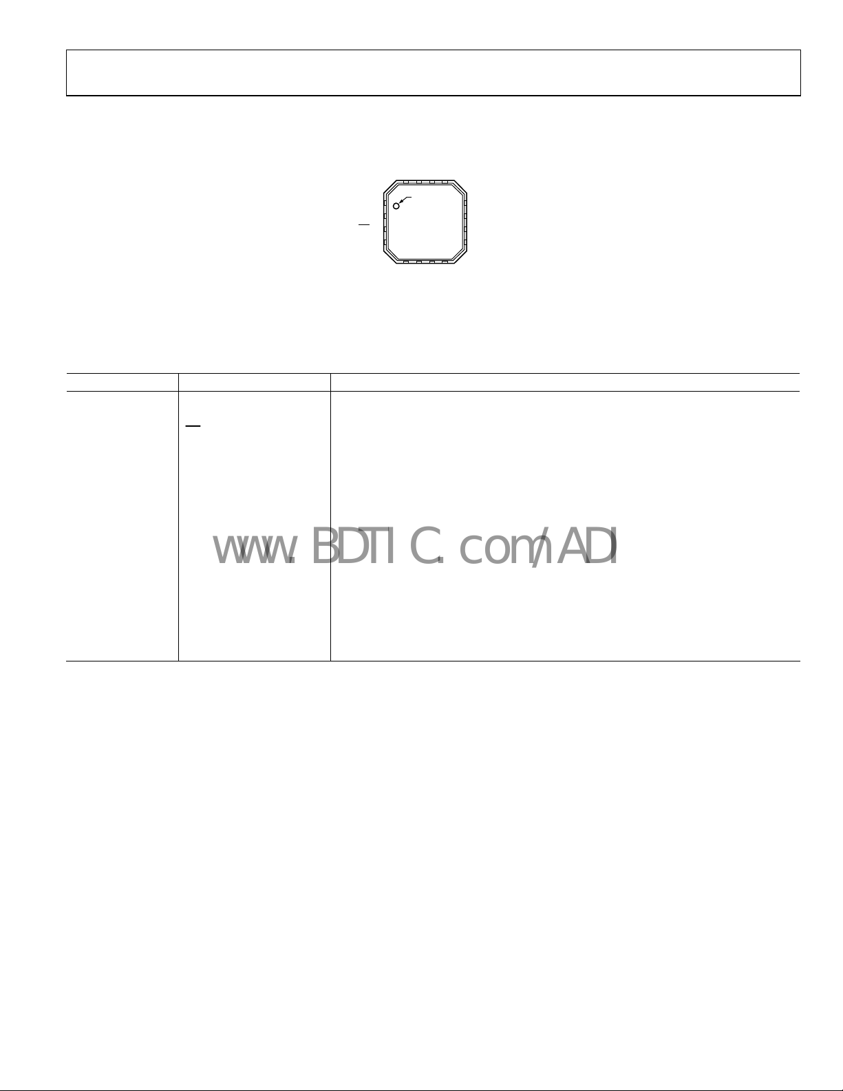
PIN CONFIGURATION AND FUNCTION DESCRIPTIONS
VDD
GND
GND
VDD
14
13
15
16
PIN 1
INDICATOR
1OUTL+
2OUTL–
SSM2306
3SD
TOP VIEW
(Not to Scale)
4INL+
5
6
NC
INL–
NC = NO CONNECT
Figure 2. Pin Configuration
Table 4. Pin Function Descriptions
Pin No. Mnemonic Description
1 OUTL+ Inverting Output for Left Channel.
2 OUTL− Noninverting Output for Left Channel.
3
SD
Shutdown Input. Active low digital input.
4 INL+ Noninverting Input for Left Channel.
5 INL− Inverting Input for Left Channel.
6 NC No Connect.
7 NC No Connect.
8 INR− Inverting Input for Right Channel.
9 INR+ Noninverting Input for Right Channel.
10 NC No Connect.
11 OUTR− Noninverting Output for Right Channel.
12 OUTR+
Inverting Output for Right Channel.
13 GND Ground for Output Amplifiers.
14 VDD Power Supply for Output Amplifiers.
15 VDD Power Supply for Output Amplifiers.
16 GND Ground for Output Amplifiers.
12 OUTR+
11 OU TR–
10 NC
9 INR+
8
7
NC
INR–
06542-002
Rev. 0 | Page 5 of 16

SSM2306
www.BDTIC.com/ADI
TYPICAL PERFORMANCE CHARACTERISTICS
100
RL = 4Ω, 33µH
= 18dB
A
V
10
VDD = 2.5V
100
10
RL = 8Ω, 33µH
= 6dB
A
V
VDD = 2.5V
1
VDD = 3.6V
0.1
THD + N (%)
0.01
0.001
0.0001 10
0.001 0.01 0.1 1
OUTPUT POWER (W)
Figure 3. THD + N vs. Output Power into 4 Ω, A
100
RL = 8Ω, 33µH
A
= 18dB
V
10
1
0.1
THD + N (%)
0.01
0.001
0.0001 10
0.001 0.01 0.1 1
OUTPUT PO WER (W)
VDD = 2.5V
VDD = 3.6V
Figure 4. THD + N vs. Output Power into 8 Ω, A
VDD = 5V
= 18 dB
V
VDD = 5V
= 18 dB
V
1
VDD = 3.6V
0.1
THD + N (%)
1W
VDD = 5V
= 6 dB
V
06542-006
06542-007
0.01
0.001
06542-003
0.001 0.010.0001 10
OUTPUT POWER (W)
0.1 1
Figure 6. THD + N vs. Output Power into 8 Ω, A
100
VDD = 5V
R
= 8Ω, 33µH
L
= 18dB
A
V
10
1
0.1
THD + N (%)
0.01
0.001
10 100k
06542-004
100 1k 10k
Figure 7. THD + N vs. Frequency, V
0.25W
FREQUENCY (Hz)
= 5 V, RL = 8 Ω, AV = 18 dB
DD
0.5W
100
RL = 4Ω, 33µH
A
= 6dB
V
10
1
0.1
THD + N (%)
0.01
0.001
0.0001 10
0.001 0.01 0.1 1
OUTPUT PO WER (W)
Figure 5. THD + N vs. Output Power into 4 Ω, A
VDD = 2.5V
VDD = 3.6V
VDD = 5V
= 6 dB
V
06542-005
Rev. 0 | Page 6 of 16
100
VDD = 5V
A
= 18dB
V
R
= 4Ω, 33µH
L
10
1
0.1
THD + N (%)
0.01
0.001
10 100 1k 10k 100k
FREQUENCY (Hz)
Figure 8. THD + N vs. Frequency, V
2W
1W
0.5W
= 5 V, RL = 4 Ω, AV = 18 dB
DD
06542-008

SSM2306
www.BDTIC.com/ADI
100
VDD = 3.6V
A
= 18dB
V
R
= 8Ω, 33µH
L
10
1
0.1
THD + N (%)
0.01
0.001
10 100 1k 10k 100k
Figure 9. THD + N vs. Frequency, V
100
VDD = 3.6V
= 18dB
A
V
= 4Ω, 33µH
R
L
10
1
0.1
THD + N (%)
0.01
FREQUENCY (Hz)
= 3.6 V, RL = 8 Ω, AV = 18 dB
DD
1W
0.5W
0.25W
0.25W
0.5W
0.125W
100
VDD = 2.5V
A
= 18dB
V
= 4Ω, 33µH
R
L
10
1
0.1
THD + N (%)
0.01
0.001
10 100 1k 10k 100k
06542-009
FREQUENCY (Hz)
Figure 12. THD + N vs. Frequency, V
7.5
ISY FOR BOTH CHANNEL S
7.0
6.5
6.0
5.5
5.0
SUPPLY CURRENT (mA)
4.5
RL = 8Ω, 33µH
RL = 4Ω, 33µH
0.5W
0.125W
0.25W
= 2.5 V, RL = 4 Ω, AV = 18 dB
DD
NO LOAD
6542-012
0.001
10 100 1k 10k 100k
FREQUENCY (Hz)
Figure 10. THD + N vs. Frequency, V
100
VDD = 2.5V
= 18dB
A
V
= 8Ω, 33µH
R
L
10
1
0.1
THD + N (%)
0.01
0.001
10 100 1k 10k 100k
FREQUENCY (Hz)
Figure 11. THD + N vs. Frequency, V
= 3.6 V, RL = 4 Ω, AV = 18 dB
DD
0.25W
0.125W
= 2.5 V, RL = 8 Ω, AV = 18 dB
DD
0.075W
4.0
2.5 3.0 3.5 4.0 4.5 5.0 5.5
06542-010
SUPPLY VOLTAGE (V)
06542-013
Figure 13. Supply Current vs. Supply Voltage, No Load
12
10
8
6
4
SUPPLY CURRENT (µA)
2
0
0 0.10.20.30.40.50.60.70.8
6542-011
SHUTDOWN VO LTAGE ( V)
VDD = 5V
VDD = 3.6V
VDD = 2.5V
06542-014
Figure 14. Supply Current vs. Shutdown Voltage
Rev. 0 | Page 7 of 16

SSM2306
www.BDTIC.com/ADI
3.0
f = 1kHz
= 18dB
A
V
R
= 4Ω, 33µH
L
2.5
2.0
1.5
1.0
OUTPUT PO WER (W)
0.5
0
2.5 3.0 3.5 4.0 4.5 5.0
SUPPLY VOLTAGE (V)
Figure 15. Maximum Output Power vs. Supply Voltage, R
10%
1%
= 4 Ω, AV = 18 dB
L
1.8
f = 1kHz
= 6dB
A
V
1.6
R
= 8Ω, 33µH
L
1.4
1.2
1.0
0.8
0.6
OUTPUT PO WER (W)
0.4
0.2
0
2.53.03.54.04.55.0
6542-015
SUPPLY VOLTAGE (V)
Figure 18. Maximum Output Power vs. Supply Voltage, R
10%
1%
= 8 Ω, AV = 6 dB
L
6542-018
3.0
f = 1kHz
A
= 6dB
V
= 4Ω, 33µH
R
L
2.5
2.0
1.5
1.0
OUTPUT PO WER (W)
0.5
0
2.5 3.0 3.5 4.0 4.5 5.0
SUPPLY VOLTAGE (V)
10%
1%
Figure 16.Maximum Output Power vs. Supply Voltage, R
1.8
f = 1kHz
A
= 18dB
V
1.6
= 8Ω, 33µH
R
L
1.4
1.2
1.0
0.8
0.6
OUTPUT POW ER (W)
0.4
0.2
0
2.5 3.0 3.5 4.0 4.5 5.0
10%
1%
SUPPLY VOLTAGE (V)
Figure 17. Maximum Output Power vs. Supply Voltage, R
= 4 Ω, AV = 6 dB
L
= 8 Ω, AV = 18 dB
L
100
RL = 4Ω, 33µH
90
80
70
60
50
40
EFFICIENCY (%)
30
20
10
06542-016
V
= 2.5V
DD
0
0 0.2 0.4 0.6 0.8 1.0 1.2 1.4 1.6 1.8 2.0
= 3.6V
V
DD
OUTPUT PO WER (W)
VDD = 5V
06542-019
Figure 19. Efficiency vs. Output Power into 4 Ω
100
RL = 8Ω, 33µH
90
80
70
V
DD
60
50
40
EFFICIENCY (%)
30
20
10
0
0
0.20.40.60.81.01.21.41.61.8
06542-017
= 2.5V
V
= 3.6V
DD
OUTPUT PO WER (W)
VDD = 5V
06542-020
Figure 20. Efficiency vs. Output Power into 8 Ω
Rev. 0 | Page 8 of 16

SSM2306
www.BDTIC.com/ADI
1.4
VDD = 5V
R
= 8Ω, 33µH
L
1.2
FOR BOTH CHANNEL S
1.0
0.8
0.6
0.4
POWER DISSIPATIO N (W)
0.2
0
0 0.1 0.2 0.3 0.4 0.5 0.6 0.7 0.8 0.9 1.0 1.1
OUTPUT PO WER (W)
Figure 21. Power Dissipation vs. Output Power at V
DD
= 5 V, RL = 8 Ω
06542-021
2.2
VDD = 3.6V
R
= 4Ω, 33µH
2.0
L
FOR BOTH CHANNELS
1.8
1.6
1.4
1.2
1.0
0.8
0.6
POWER DISSIPATIO N (W)
0.4
0.2
0
0 0.10.20.30.40.50.60.70.80.91.01.11.21.31.41.51.6
OUTPUT PO WER (W)
Figure 24. Power Dissipation vs. Output Power at V
= 3.6 V, RL = 4 Ω
DD
06542-024
1.0
VDD = 3.6V
0.9
= 8Ω, 33µH
R
L
FOR BOTH CHANNEL S
0.8
0.7
0.6
0.5
0.4
0.3
POWER DISSIPATION (W)
0.2
0.1
0
0 0.10.20.30.40.50.60.70.8
OUTPUT PO WER (W)
Figure 22. Power Dissipation vs. Output Power at V
2.8
VDD = 5V
2.6
R
= 4Ω, 33µH
L
2.4
FOR BOTH CHANNELS
2.2
2.0
1.8
1.6
1.4
1.2
1.0
0.8
POWE R DISSI PATI ON (W)
0.6
0.4
0.2
0
0 0.2 0.4 0.6 0.8 1.0 1.2 1.4 1.6 1.8 2.0 2.2
OUTPUT PO WER (W)
Figure 23. Power Dissipation vs. Output Power at V
= 3.6 V, RL = 8 Ω
DD
= 5 V, RL = 4 Ω
DD
900
= 8Ω, 33µH
R
L
I
IS FOR BOT H CHANNELS
SY
800
700
600
500
(mA)
400
SY
I
300
200
100
0
0 0.2 0.4 0.6 0.8 1.0 1. 2 1.4 1.6
6542-022
V
= 2.5V
DD
V
DD
PO (W)
= 3.6V
VDD = 5V
06542-025
Figure 25. Supply Current vs. Output Power into 8 Ω
1300
R
= 4Ω, 33µH
L
1200
I
IS FOR BOT H CHANNELS
SY
1100
1000
900
800
700
(mA)
600
SY
I
500
400
300
200
100
0
0 0.2 0.4 0.6 0.8 1.0 1.2 1.4 1.6 1.8 2.0 2.2
06542-023
V
DD
= 2.5V
PO (W)
= 3.6V
V
DD
VDD = 5V
06542-026
Figure 26. Supply Current vs. Output Power into 4 Ω
Rev. 0 | Page 9 of 16

SSM2306
www.BDTIC.com/ADI
0
–10
–20
–30
–40
–50
PSRR (dB)
–60
–70
–80
–90
–100
10 100 1k 10k 100k
7
6
5
4
FREQUENCY (Hz)
3
2
VOLTAGE (V)
1
0
–1
–2
–100 102030405060708090
06542-027
SD INPUT
OUTPUT
TIME (ms)
Figure 27. PSRR vs. Frequency Figure 30. Turn-On Response
06542-030
0
RL = 8Ω, 33µH
–10
–20
–30
–40
CMRR (dB)
–50
–60
–70
–80
10 100 1k 10k 100k
FREQUENCY (Hz)
Figure 28. CMRR vs. Frequency
0
VDD = 3.6V
V
= 1V rms
RIPPLE
R
= 8Ω, 33µH
–20
L
–40
–60
–80
CROSSTALK (dB)
–100
7
6
SD INPUT
5
4
3
2
VOLTAGE (V)
1
0
–1
–2
–20 0 20 40 60 80 100 120 140 160 180
06542-028
OUTPUT
TIME (ms)
6542-031
Figure 31. Turn-Off Response
–120
–140
10 100 1k 10k 100k
FREQUENCY (Hz)
06542-029
Figure 29. Crosstalk vs. Frequency
Rev. 0 | Page 10 of 16

SSM2306
www.BDTIC.com/ADI
TYPICAL APPLICATION CIRCUITS
10µF
SSM2306
1
22nF
R
EXT
RIGHT IN+
RIGHT IN–
SHUTDOWN
LEFT IN+
LEFT IN–
1
INPUT CAPS ARE O PTIONAL IF INPUT DC COMMON-M ODE
VOLTAGE IS APPROXIMATELY V
22nF
22nF
22nF
1
1
1
INR+
INR–
R
EXT
SD
R
EXT
INL+
INL–
R
EXT
/2.
DD
BIAS
Figure 32. Stereo Differential Input Configuration
10µF
0.1µF
MODULATOR
INTERNAL
OSCILLATOR
MODULATOR
0.1µF
VBATT
2.5V TO 5. 0V
VDDVDD
FET
DRIVER
FET
DRIVER
GNDGND
VBATT
2.5V TO 5. 0V
OUTR+
OUTR–
OUTL+
OUTL–
6542-037
RIGHT IN
SHUTDOWN
LEFT IN
22nF
22nF
22nF
22nF
SSM2306
R
EXT
INR+
INR–
R
EXT
SD
R
EXT
INL+
INL–
R
EXT
BIAS
MODULATOR
INTERNAL
OSCILLATOR
MODULATOR
Figure 33. Stereo Single-Ended Input Configuration
VDDVDD
DRIVER
DRIVER
GNDGND
FET
FET
OUTR+
OUTR–
OUTL+
OUTL–
6542-038
Rev. 0 | Page 11 of 16

SSM2306
www.BDTIC.com/ADI
APPLICATION NOTES
OVERVIEW
The SSM2306 stereo, Class-D, audio amplifier features a filterless
modulation scheme that greatly reduces the external components count, conserving board space and, thus, reducing systems
cost. The SSM2306 does not require an output filter; instead, it
relies on the inherent inductance of the speaker coil and the
natural filtering capacity of the speaker and human ear to fully
recover the audio component of the square wave output.
Although most Class-D amplifiers use some variation of pulse-
idth modulation (PWM), the SSM2306 uses sigma-delta (Σ-Δ)
w
modulation to determine the switching pattern of the output
devices. This provides a number of important benefits. Σ-Δ
modulators do not produce a sharp peak with many harmonics
in the AM frequency band, as pulse-width modulators often do.
Σ-Δ modulation provides the benefits of reducing the amplitude
of spectral components at high frequencies; that is, reducing EMI
emission that might otherwise radiate by the use of speakers
and long cable traces. The SSM2306 also offers protection
circuits for overcurrent and overtemperature protection.
EMI NOISE
The SSM2306 uses a proprietary modulation and spreadspectrum technology to minimize EMI emissions from the
device. Figure 34 shows SSM2306 EMI emission starting from
100 kH
z to 30 MHz. Figure 35 shows SSM2306 EMI emission
f
rom 30 kHz to 2 GHz. These figures clearly depict the SSM2306
EMI behavior as being well below the FCC regulation values,
starting from 100 kHz and passing beyond 1 GHz of frequency.
Although the overall EMI noise floor is slightly higher, frequency
spurs from the SSM2306 are greatly reduced.
70
= HORIZONTAL
= VERTICAL
= REGULATION VALUE
60
50
40
30
LEVEL (dB(µV/m))
20
GAIN SELECTION
The SSM2306 has a pair of internal resistors that set an 18 dB
default gain for the amplifier. It is possible to adjust the SSM2306
gain by using external resistors at the input. To set a gain lower
than 18 dB, refer to Figure 32 for the differential input configur
ation and Figure 33 for the single-ended configuration. Calculate
t
he external gain configuration as
External Gain Settings = 344 kΩ/(43 kΩ + R
EXT
)
POP-AND-CLICK SUPPRESSION
Voltage transients at the output of audio amplifiers can occur with
the activation or deactivation of shutdown. Furthermore, voltage
transients as low as 10 mV are audible as an audio pop in the
speaker. Likewise, clicks and pops are classified as undesirable
audible transients generated by the amplifier system, and as
such, as not coming from the system input signal. These types
of transients generate when the amplifier system changes its
operating mode. For example, the following can be sources of
audible transients:
ystem power-up/power-down
• S
• Mu
• Inp
• Sa
The SSM2306 has a pop-and-click suppression architecture that
r
deactivation.
te/unmute
ut source change
mple rate change
educes these output transients, resulting in noiseless activation and
10
0
0.1 100
Figure 34. EMI Emissions from SSM2306
70
= HORIZONTAL
= VERTICAL
= REGULATION VALUE
60
50
40
30
LEVEL (dB(µV/m))
20
10
0
10 10k
Figure 35. EMI Emissions from SSM2306
110
FREQUENCY (M Hz)
100 1k
FREQUENCY (M Hz)
06542-039
06542-040
The measurements for Figure 34 and Figure 35 were taken with
a 1 kHz input signal, producing 0.5 W output power into an 8 Ω
load from a 3.6 V supply. Cable length was approximately 5 cm.
To detect EMI, a magnetic probe was used touching the 2-inch
output trace to the load.
Rev. 0 | Page 12 of 16

SSM2306
www.BDTIC.com/ADI
LAYOUT
As output power continues to increase, careful layout is needed
for proper placement of PCB traces and wires between the amplifier, load, and power supply. A good practice is to use short, wide
PCB tracks to decrease voltage drops and minimize inductance.
Make track widths at least 200 mil for every inch of track length
for lowest DCR, and use 1 oz. or 2 oz. of copper PCB traces to
further reduce IR drops and inductance. Poor layout increases
voltage drops, consequently affecting efficiency. Use large traces
for the power supply inputs and amplifier outputs to minimize
losses due to parasitic trace resistance. Proper grounding guidelines help to improve audio performance, minimize crosstalk
between channels, and prevent switching noise from coupling
into the audio signal.
To maintain high output swing and high peak output power, the
PCB t
races that connect the output pins to the load and supply
pins should be as wide as possible to maintain the minimum
trace resistances. It is also recommended to use a large area
ground plane for minimum impedances.
Good PCB layouts isolate critical analog paths from sources of
h interference; furthermore, separate high frequency circuits
hig
(analog and digital) from low frequency ones. Properly designed
multilayer printed circuit boards can reduce EMI emission and
increase immunity to RF field by a factor of 10 or more compared
with double-sided boards. A multilayer board allows a complete
layer to be used for the ground plane, whereas the ground plane
side of a double-sided board is often disrupted with signal crossover. If the system has separate analog and digital ground and
power planes, the analog ground plane should be underneath
the analog power plane, and, similarly, the digital ground plane
should be underneath the digital power plane. There should be
no overlap between analog and digital ground planes or analog
and digital power planes.
INPUT CAPACITOR SELECTION
The SSM2306 does not require input coupling capacitors if the
input signal is biased from 1.0 V to V
are required if the input signal is not biased within this recommended input dc common-mode voltage range, if high-pass
filtering is needed (see
urce (see Figure 33). If high-pass filtering is needed at the
so
in
put, the input capacitor together with the input resistor of the
SSM2306 form a high-pass filter whose corner frequency is
determined by the following equation:
= 1/(2π × RIN × CIN)
f
C
Input capacitors can have very important effects on the circuit
p
erformance. Not using input capacitors degrades the output
offset of the amplifier as well as the PSRR performance.
Figure 32), or if using a single-ended
− 1.0 V. Input capacitors
DD
PROPER POWER SUPPLY DECOUPLING
To ensure high efficiency, low total harmonic distortion (THD),
and high PSRR, proper power supply decoupling is necessary.
Noise transients on the power supply lines are short duration
voltage spikes. Although the actual switching frequency can
range from 10 kHz to 100 kHz, these spikes can contain frequency components that extend into the hundreds of megahertz.
The power supply input needs to be decoupled with a good
quality, low ESL and low ESR capacitor, usually around 4.7 μF.
This capacitor bypasses low frequency noises to the ground
plane. For high frequency transients noises, use a 0.1 μF capacitor
as close as possible to the VDD pin of the device. Placing the
decoupling capacitor as close as possible to the SSM2306 helps
maintain efficiency performance.
Rev. 0 | Page 13 of 16

SSM2306
R
R
www.BDTIC.com/ADI
OUTLINE DIMENSIONS
INDICATO
SEATING
PIN 1
0.90
0.85
0.80
PLANE
12° MAX
3.00
BSC SQ
TOP
VIEW
0.30
0.23
0.18
*
COMPLIANT
EXCEPT FOR EXPOSED PAD DIMENSION.
2.75
BSC SQ
0.80 MAX
0.65 TYP
0.05 MAX
0.02 NOM
0.20 REF
TO
JEDEC STANDARDS MO-220-VEED-2
0.45
0.50
BSC
1.50 REF
0.60 MAX
12
9
13
EXPOSED
PAD
(BOTTOM VIEW)
8
Figure 36. 16-Lead Lead Frame Chip Scale Package [LFCSP_VQ]
3
mm × 3 mm Body, Very Thin Quad
(CP-16-3)
Dimensions shown in millimeters
0.50
0.40
0.30
16
1
4
5
N
P
I
D
N
I
*
1.65
1.50 SQ
1.35
0.25 MIN
1
O
C
I
A
T
ORDERING GUIDE
Model Temperature Range Package Description Package Option Branding
SSM2306CPZ-R2
SSM2306CPZ-REEL
SSM2306CPZ-REEL7
1
Z = RoHS Compliant Part.
1
−40°C to +85°C 16-Lead Lead Frame Chip Scale Package [LFCSP_VQ] CP-16-3 A1R
1
−40°C to +85°C 16-Lead Lead Frame Chip Scale Package [LFCSP_VQ] CP-16-3 A1R
1
−40°C to +85°C 16-Lead Lead Frame Chip Scale Package [LFCSP_VQ] CP-16-3 A1R
Rev. 0 | Page 14 of 16

SSM2306
www.BDTIC.com/ADI
NOTES
Rev. 0 | Page 15 of 16

SSM2306
www.BDTIC.com/ADI
NOTES
©2007 Analog Devices, Inc. All rights reserved. Trademarks and
registered trademarks are the property of their respective owners.
D06542-0-4/07(0)
Rev. 0 | Page 16 of 16
 Loading...