

Page 1
a
Trimless
Voltage Controlled Amplifiers
FEATURES
117 dB Dynamic Range
0.006% Typical THD+N (@ 1 kHz, Unity Gain)
140 dB Gain Range
No External Trimming Required
Differential Inputs
Complementary Gain Outputs
Buffered Control Port
I–V Converter On-Chip
Low External Parts Count
Low Cost
GENERAL DESCRIPTION
The SSM2018T represents continuing evolution of the Frey
Operational Voltage Controlled Element (OVCE) topology that
permits flexibility in the design of high performance volume
control systems. The SSM2018T is laser trimmed for gain core
symmetry and offset. As a result, the SSM2018T is the first
professional audio quality VCA to offer trimless operation.
Due to careful gain core layout, the SSM2018T combines the
low noise of Class AB topologies with the low distortion of
Class A circuits to offer an unprecedented level of sonic trans-
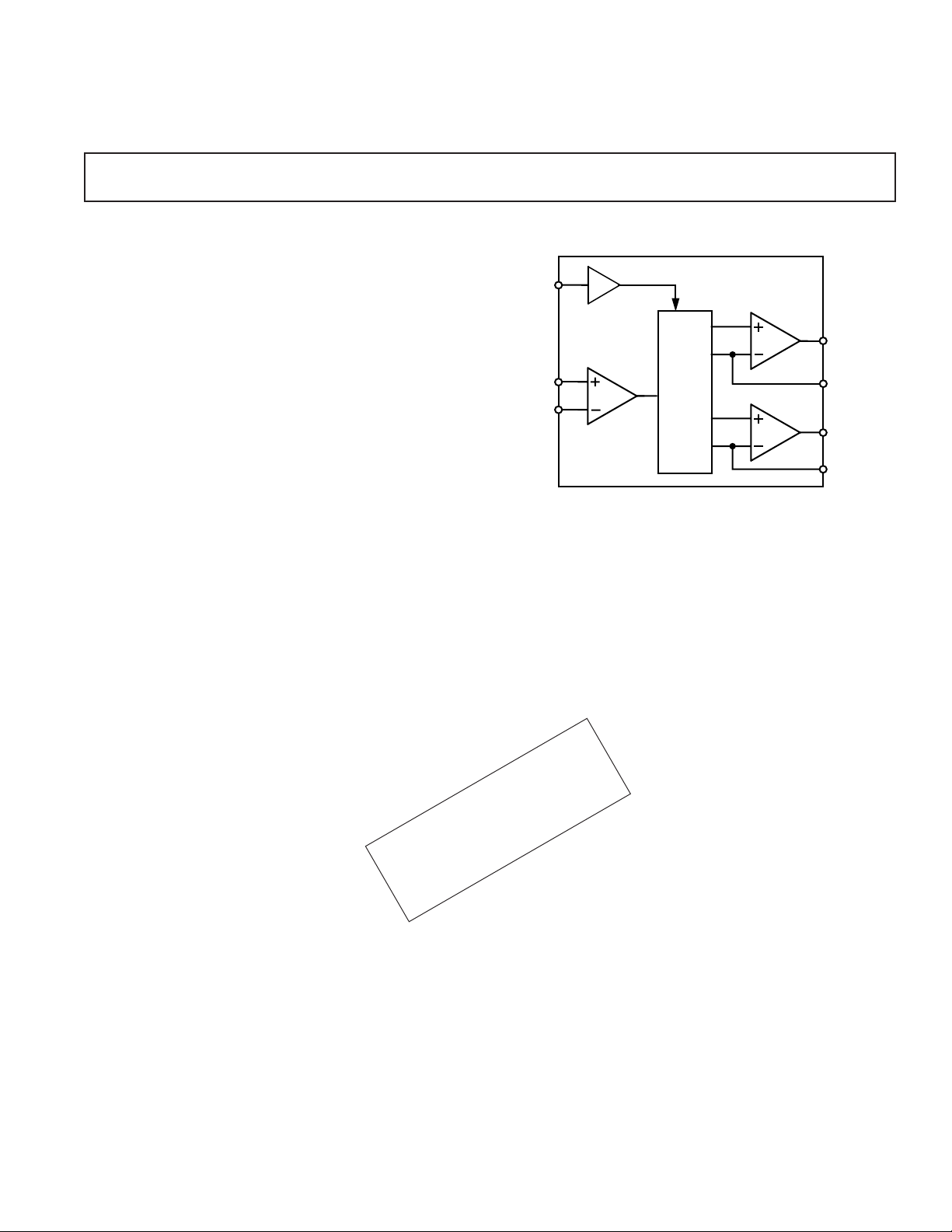
SSM2018T
FUNCTIONAL BLOCK DIAGRAM
V
C
+IN
–IN
parency. Additional features include differential inputs, a 140 dB
(–100 dB to +40 dB) gain range and a high impedance control
port. The SSM2018T provides an internal current-to-voltage
converter. Thus no external active components are required.
This device is offered in 16-lead plastic DIP and SOIC packages
and guaranteed for operation over the extended industrial temperature range of –40∞C to +85∞C.
GAIN
CORE
SSM2018T
G
1–G
*
V
G
–I
G
V
1–G
–I
1–G
NEW E GRADE
0.01% THD+N MAX
*Protected by U.S. Patent Nos. 4,471,320 and 4,560,947.
REV. B
Information furnished by Analog Devices is believed to be accurate and
reliable. However, no responsibility is assumed by Analog Devices for its
use, nor for any infringements of patents or other rights of third parties that
may result from its use. No license is granted by implication or otherwise
under any patent or patent rights of Analog Devices.
One Technology Way, P.O. Box 9106, Norwood, MA 02062-9106, U.S.A.
Tel: 781/329-4700 www.analog.com
Fax: 781/326-8703 ©Analog Devices, Inc., 2002
Page 2

SSM2018T–SPECIFICATIONS
ELECTRICAL SPECIFICATIONS
(VS = ⴞ15 V, AV = 0 dB, RL = 100 k⍀, f = 1 kHz, 0 dBu = 0.775 V rms, simple VCA application
circuit with 18 k⍀ resistors, –VIN floating, and Class AB gain core bias (RB = 150 k⍀), –40ⴗC < TA < +85ⴗC, unless otherwise noted. Typical
specifications apply at TA = 25ⴗC.)
Parameter Conditions Min Typ Max Max (E Grade) Unit
AUDIO PERFORMANCE
Noise VIN = GND, 20 kHz Bandwidth –95 –93 dBu
Headroom Clip Point = 1% THD + N 22 dBu
Total Harmonic Distortion plus Noise 2nd and 3rd Harmonics Only
(25∞Cto85∞C)
AV = 0 dB, VIN = +10 dBu 0.006 0.020 0.01 %
= +20 dB, VIN = –10 dBu 0.013 0.03 0.02 %
A
V
AV = –20 dB, VIN = +10 dBu 0.013 0.03 0.02 %
INPUT AMPLIFIER
Bias Current V
Offset Voltage V
Offset Current V
Input Impedance 4 MW
Common-Mode Range ± 13 V
Gain Bandwidth VCA Configuration 0.7 MHz
Slew Rate 5V/ms
OUTPUT AMPLIFIER
Offset Voltage VIN = 0 V, VC = 4 V 1.0 15 mV
Output Voltage Swing I
Minimum Load Resistance For Full Output Swing 9 kW
CONTROL PORT
Bias Current 0.36 1 mA
Input Impedance 1 MW
Gain Constant Device Powered in Socket > 60 sec –30 mV/dB
Gain Constant Temperature Coefficient –3500 ppm/∞C
Control Feedthrough 0 dB to –40 dB Gain Range ± 1 ±4 ± 3mV
Maximum Gain V
Maximum Attenuation VC = 4 V 100 dB
POWER SUPPLIES
Supply Voltage Range ± 5 ± 18 V
Supply Current 11 15 mA
Power Supply Rejection Ratio 80 dB
= 0 V 0.25 1 mA
CM
= 0 V 1 15 mV
CM
= 0 V 10 100 nA
CM
VCP Configuration 14 MHz
= 1.5 mA
OUT
Positive 10 13 V
Negative –10 –14 V
= –1.3 V 40 mV
C
Specifications subject to change without notice.
–2–
REV. B
Page 3
SSM2018T
WARNING!
ESD SENSITIVE DEVICE
ABSOLUTE MAXIMUM RATINGS
1
Supply Voltage
Dual Supply . . . . . . . . . . . . . . . . . . . . . . . . . . . . . . . . .±18 V
Input Voltage . . . . . . . . . . . . . . . . . . . . . . . . . . . . . . . . . . . ± V
S
Operating Temperature Range . . . . . . . . . . . .–40∞C to +85∞C
Storage Temperature . . . . . . . . . . . . . . . . . . . –65∞C to +150∞C
Junction Temperature (T
) . . . . . . . . . . . . . . . . . . . . . . 150∞C
J
Lead Temperature (Soldering, 60 sec) . . . . . . . . . . . . . 300∞C
THERMAL CHARACTERISTICS
Thermal Resistance
2
16-Lead Plastic DIP
. . . . . . . . . . . . . . . . . . . . . . . . . . . . . . . . . . . . . . 76∞C/W
JA
. . . . . . . . . . . . . . . . . . . . . . . . . . . . . . . . . . . . . . 33∞C/W
JC
16-Lead SOIC
. . . . . . . . . . . . . . . . . . . . . . . . . . . . . . . . . . . . . . 92∞C/W
JA
. . . . . . . . . . . . . . . . . . . . . . . . . . . . . . . . . . . . . . 27∞C/W
JC
TRANSISTOR COUNT
Number of Transistors
SSM2018T . . . . . . . . . . . . . . . . . . . . . . . . . . . . . . . . . . 125
ESD RATINGS
883 (Human Body) Model . . . . . . . . . . . . . . . . . . . . . . . 500 V
EIAJ Model . . . . . . . . . . . . . . . . . . . . . . . . . . . . . . . . . . . 100 V
NOTES
1
Stresses above those listed under Absolute Maximum Ratings may cause perma-
nent damage to the device. This is a stress rating only; functional operation of the
device at these or any other conditions above those indicated in the operation
section of this specification is not implied. Exposure to absolute maximum rating
conditions for extended periods may affect device reliability.
2
JA is specified for worst-case conditions, i.e.; JA is specified for device in socket for
P-DIP and device soldered in circuit board for SOIC package.
ORDERING GUIDE
Model Temperature Range Package Option
1
SSM2018TP –40∞C to +85∞C N-16
SSM2018TS2–40∞C to +85∞C R-16
1
N = Plastic DIP; R = SOL.
2
Not for new designs; obsolete April 2002.
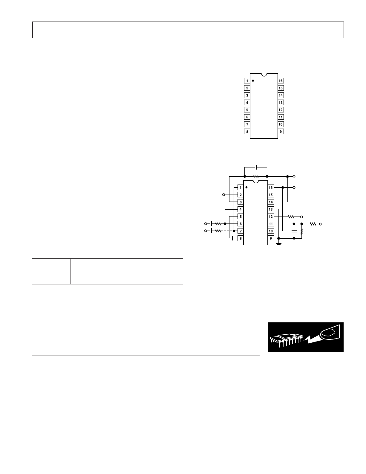
PIN CONFIGURATION
16-Lead Plastic DIP
and SOL
+I
1–G
V+
–I
G
1–G
+IN
–IN
SSM2018T
TOP VIEW
(Not to Scale)
50pF
18k
SSM2018T
–I
COMP 1
COMP 2 COMP 3
V+
1F
V
V
18k
IN+
IN–
18k
1F
47pF
V
1–G
BAL
V
G
GND
MODE
V
C
V–
150k
1F
V
OUT
V–
V+
V
CONTROL
3k
1k
SSM2018T Typical Application Circuit
CAUTION
ESD (electrostatic discharge) sensitive device. Electrostatic charges as high as 4000 V readily
accumulate on the human body and test equipment and can discharge without detection.
Although the SSM2018T features proprietary ESD protection circuitry, permanent damage may
occur on devices subjected to high-energy electrostatic discharges. Therefore, proper ESD precautions are recommended to avoid performance degradation or loss of functionality.
REV. B
–3–
Page 4
SSM2018T–Typical Performance Characteristics
0.1
TA = +25ⴗC
= ⴞ15V
V
S
R
= 18k⍀
F
0.010
THD + N – %
0.001
20 10k
FREQUENCY – Hz
AV = +20dB
AV = –20dB
AV = 0dB
1k100 20k
A
TPC 1. SSM2018T THD + N Frequency (80 kHz Low-Pass
Filter, for A
= 0.3 V rms; for AV = –20 dB, VIN = 3 V rms)
V
IN
= 0 dB, VIN = 3 V rms; for AV = +20 dB,
V
0.1
TA = +25ⴗC
= ⴞ15V
V
S
= 18k⍀
R
F
0.010
THD + N – %
0.001
10m 1
0.1 2
AMPLITUDE – V
RMS
TPC 4. SSM2018T THD + N vs. Amplitude
(Gain = +20 dB, f
1.0
0.1
=1 kHz, 80 kHz Low-Pass Filter)
IN
TA = +25ⴗC
V
= ⴞ15V
S
R
= 18k⍀
F
A
TPC 2. SSM2018T Distortion Distribution
0.1
TA = +25ⴗC
R
= 18k⍀
F
= ⴞ15V
V
S
0.1
THD + N – %
0.010
0.001
0.1 10
120
AMPLITUDE – V
RMS
A
TPC 3. SSM2018T THD + N vs. Amplitude (Gain = 0 dB,
= 1 kHz, 80 kHz Low-Pass Filter)
f
IN
THD + N – %
0.01
0.001
–60 –40 20–20
GAIN – dB
040
TPC 5. SSM2018T THD + N vs. Gain (fIN = 1 kHz;
£
for –60 dB
for 0 dB
0.1
0.01
THD + N – %
0.001
AV £ –20 dB, VIN = 10 V rms;
£
AV £ +20 dB, VIN = 1 V rms)
TA = +25ⴗC
= 18k⍀
R
F
ⴞ5
ⴞ6 ⴞ9 ⴞ15 ⴞ18
SUPPLY VOLTAGE – Volts
ⴞ12
TPC 6. SSM2018T THD + N vs. Supply Voltage
(A
= 0 dB, VIN = 1 V rms, fIN = 1 kHz, 80 kHz
V
Low-Pass Filter)
–4–
REV. B
Page 5
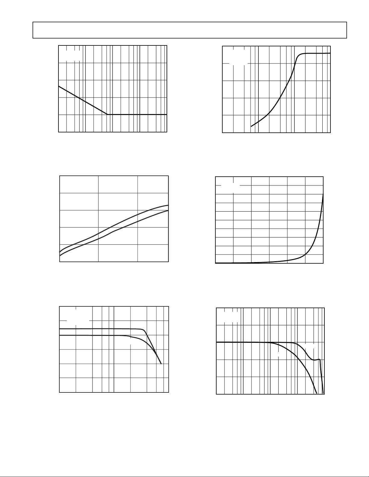
SSM2018T
LOAD RESISTANCE – ⍀
MAXIMUM OUTPUT SWING – V
PEAK
ⴞ15
ⴞ12
0
100 1k 100k10k
ⴞ9
ⴞ6
ⴞ3
RF = 18k⍀
T
A
= +25ⴗC
VS = ⴞ15V
+10
0
–15
1k 1M100k10k100
–5
–10
+5
FREQUENCY – Hz
TA = +25ⴗC
V
S
= ⴞ15V
GAIN – dB
0
–135
–45
–90
PHASE – Degrees
GAIN
PHASE
500
TA = +25ⴗC
V
= ⴞ15V
S
400
300
200
NOISE DENSITY – nV/冪Hz
100
0
100 100k10k1k10
FREQUENCY – Hz
TPC 7. SSM2018T Noise Density vs. Frequency
(Unity Gain, Referred to Input)
RF = ⴥ⍀
= +25ⴗC
T
A
ⴞ20
PEAK
ⴞ15
RL = ⴥ
ⴞ10
RL = 10k⍀
ⴞ5
OUTPUT VOLTAGE SWING – V
0
ⴞ5
SUPPLY VOLTAGE – Volts
TPC 8. SSM2018T Maximum Output Swing vs.
Supply Voltage (THD = 1% max)
TPC 10. SSM2018T Maximum Output Swing vs.
Load Resistance (THD = 1 % max)
100
TA = +25ⴗC
90
V
= ⴞ15V
S
80
70
60
50
40
30
OUTPUT OFFSET – mV
20
10
ⴞ18 ⴞ15 ⴞ10
0
–80
–60
GAIN – dB
40
200–20–40
TPC 11. SSM2018T Typical Output Offset vs. Gain
ⴞ15
PEAK
ⴞ12
ⴞ9
ⴞ6
ⴞ3
MAXIMUM OUTPUT SWING – V
0
1k 10k 100k
TPC 9. SSM2018T Maximum Output Swing vs.
Frequency (THD = 1 % max)
REV. B
RF = ⴥ⍀
= +25ⴗC
T
A
= ⴞ15V
V
S
RL = ⴥ
RL = 10k
FREQUENCY – Hz
TPC 12. SSM2018T Gain/Phase vs. Frequency
–5–
Page 6

SSM2018T
60
40
20
0
–20
GAIN – dB
–40
–60
–80
100 1k 10M1M100k10k
FREQUENCY – Hz
TPC 13. SSM2018T Gain vs. Frequency
0.06
0.05
0.04
0.03
DISTORTION – %
0.02
VIN = 10dBu
A
0.01
= 0dB
V
VIN = 10dBu
A
= –20dB
V
AND
V
= –10dBu
IN
A
= 20dB
V
TA = +25ⴗC
V
= ⴞ15V
S
TA = +25ⴗC
V
= ⴞ15V
S
TPC 16. SSM2018T Control Feedthrough Distribution
0
VS = ⴞ15V
T
= +25ⴗC
A
V
= 100mV
C
–20
–40
–60
–80
CONTROL FEEDTHROUGH – dB
RMS
0
–20
–40
TEMPERATURE – ⴗC
804020060
TPC14. SSM2018T Distortion vs. Temperature
–60
TA = +25ⴗC
V
= ⴞ15V
–40
S
GAIN – dB
200–20
–70
–80
–90
OUTPUT NOISE – dBu
–100
–110
–60
TPC 15. SSM2018T Output Noise vs. Gain
= GND, 20 kHz Bandwidth)
(V
IN
100
–100
100 1k 100k10k
FREQUENCY – Hz
Figure 17. SSM2018T Control Feedthrough vs. Frequency
3
VS = ⴞ15V
⬍ 1.2V
2
1
0
–1
–2
CONTROL FEEDTHROUGH – mV
–3
–20
40
–40
0
TEMPERATURE – ⴗC
0V ⬍ V
FREQ = 0Hz
4020
C
100
80
60
TPC 18. SSM2018T Control Feedthrough vs.
Temperature
–6–
REV. B
Page 7

SSM2018T
TA = +25ⴗC
15.0
0
ⴞ15
7.5
2.5
ⴞ5
5.0
0
12.5
10.0
ⴞ10
SUPPLY VOLTAGE – Volts
SLEW RATE – V/s
+ SLEW RATE
– SLEW RATE
–20
VS = ⴞ15V
–25
–30
–35
GAIN CONSTANT – mV/dB
–40
–20
–40 100
TEMPERATURE – °C
60
8040200
TPC 19. SSM2018T Gain Constant vs. Temperature
–28
TA = +25ⴗC
V
= ⴞ15V
S
–29
–30
0
VS = ⴞ15V
= +25ⴗC
T
A
–20
–40
CMRR – dB
–60
–80
–100
10
100
1k
FREQUENCY – Hz
10k
100k
TPC 22. SSM2018T CMRR vs. Frequency
–31
GAIN CONSTANT – mV/dB
–32
–33
–80
–60
GAIN – dB
60
40200–20–40
TPC 20. SSM2018T Gain Constant Linearity vs. Gain
0.1
0.0
–0.1
GAIN – dB
–0.2
–0.3
–0.4
100 1k 100k10k
TPC 21. SSM2018T Gain Flatness vs. Frequency
FREQUENCY – Hz
TA = +25ⴗC
V
= ⴞ15V
S
A
= 0dB
V
V
= 100V
IN
RMS
TPC 23. SSM2018T Slew Rate vs. Supply Voltage
0
VS = ⴞ15V
= +25ⴗC
T
A
–20
–40
–60
PSRR – dB
–80
–100
+ PSRR
100 100k10k1k10
– PSRR
FREQUENCY – Hz
TPC 24. SSM2018T PSRR vs. Frequency
REV. B
–7–
Page 8

SSM2018T
APPLICATIONS
The SSM2018T is a trimless Voltage Controlled Amplifier (VCA)
for volume control in audio systems. The SSM2018T is identical to the original SSM2018 in functionality and pinout; however, it is the first professional quality audio VCA in the
marketplace that does not require an external trimming potentiometer to minimize distortion. Instead, the SSM2018T is laser
trimmed before it is packaged to ensure the specified THD and
control feedthrough performance. This has a significant savings
in not only the cost of external trimming potentiometers, but
also the manufacturing cost of performing the trimming during
production.
Basic VCA Configuration
The primary application circuit for the SSM2018T is the basic
VCA configuration, which is shown in Figure 1. This configuration uses differential current feedback to realize the VCA. A
complete description of the internal circuitry of the VCA, and
this configuration, is given in the Theory of Operation section
below. The SSM2018T is trimmed at the factory for operation in the
basic VCA configuration with class AB biasing. Thus, for optimal
distortion and control feedthrough performance, the same configuration and biasing should be used. All of the graphs for the
SSM2018T in the data sheet have been measured using the
circuit of Figure 1.
50pF
18k
V+
SSM2018T
1F
V
V
18k
IN+
IN–
18k
1F
47pF
1F
R
150k
V
OUT
V–
B
V+
V
CONTROL
3k
1k
Figure 1. Basic VCA Application Circuit
In the simple VCA configuration, the SSM2018T inputs are at a
virtual ground. Thus, 18 kW resistors are required to convert the
input voltages to input currents. The schematic also shows ac
coupling capacitors. These are inserted to minimize dc offsets
generated by bias current through the resistors. Without the
capacitors, the dc offset due to the input bias current is typically
5 mV. The input stage has the flexibility to run either inverting,
noninverting, or balanced. The most common configuration is
to run it in the noninverting single-ended mode. If either input
is unused, the associated 18 kW resistor and coupling capacitor
should be removed to prevent any additional noise.
The common-mode rejection in balanced mode is typically
55 dB up to 1 kHz, decreasing at higher frequencies as shown in
TPC 21. To ensure good CMRR in the balanced configuration,
the input resistors must be balanced. For example, a 1% mismatch results in a CMRR of 40 dB. To achieve 55 dB, these
resistors should have an absolute tolerance match of 0.1%.
The output of the basic VCA is taken from Pin 14, which is the
output of an internal amplifier. Notice that the second voltage
output (Pin 16) is connected to the negative supply. This is
normal and actually disables that output amplifier ensuring that
it will not oscillate and cause interference problems. Shorting
the output to the negative supply does not cause the supply
current to increase. This amplifier is only used in the “OVCE”
application explained later.
The control port follows a –30 mV/dB control law. The application circuit shows a 3 kW and 1 kW resistor divider from a control
voltage. The choice of these resistors is arbitrary and could be
any values to properly scale the control voltage. In fact, these
resistors can be omitted if the control voltage has been properly
scaled. The 1 mF capacitor is in place to provide some filtering
of the control signal. Although the control feedthrough is trimmed
at the factory, the feedthrough increases with frequency (TPC
16). Thus, high frequency noise can feed through and add to
the noise of the VCA. Filtering the control signal helps minimize
this noise source.
Theory of Operation of the SSM2018T
The SSM2018T has the same internal circuitry as the original
SSM2018. The detailed diagram in Figure 2 shows the main
components of the VCA. The essence of the SSM2018T is
the gain core, which comprises two differential pairs (Q1–Q4).
When the control voltage, VC, is adjusted, current through the
gain core is steered to one side or the other of the two differential
pairs. The tail current for these differential pairs is set by the
mode bias of the VCA (Class A or AB), which is labeled as I
the diagram. I
the input voltage, labeled I
is then modulated by a current proportional to
M
. For a positive input voltage, more
S
in
M
current is steered (by the “Splitter”) to the left differential pair;
the opposite is true for a negative input.
To understand how the gain control works, a simple example is
best. Take the case of a positive control voltage on Pin 11. Notice
that the bases of Q2 and Q3 are connected to ground via a 200
W resistor. A positive control voltage produces a positive voltage
on the bases of Q1 and Q4. Concentrating on the left-most
differential pair, this raises the base voltage of Q1 above that of
Q2. Thus, more of the tail current is steered through Q1 than
through Q2. The current from the collector of Q2 flows through
the external 18 kW feedback resistor around amplifier A3. When
this current is reduced, the output voltage is also reduced. Thus,
a positive control voltage results in an attenuation of the input
signal, which explains why the gain constant is negative.
The collector currents of Q2 and Q3 produce the output voltage.
The output of Q3 is mirrored by amplifier A1 to add to the
overall output voltage. On the other hand, the collector currents
of Q1 and Q4 are used for feedback to the differential inputs.
Because Pins 6 and 4 are shorted together, any input voltage
produces an input current which flows into Pin 4. The same is
true for the inverting input, which is connected to Pin 1. The
overall feedback ensures that the current flowing through the
input resistors is balanced by the collector currents in Q1 and Q4.
Compensating the SSM2018T
The SSM108 has a network that uses an adaptive compensation
scheme that adjusts the optimum compensation level for a given
gain. The control voltage not only adjusts the gain core steering,
it also adjusts the compensation. The SSM2018T has three
compensation pins: COMP1, COMP2, and COMP3. COMP3
is normally left open. Grounding this pin actually defeats the adaptive compensation circuitry, giving the VCA a fixed compensation
point. The only time this is desirable is when the VCA has fixed
feedback, such as the Voltage Controlled Panner (VCP) circuit
–8–
REV. B
Page 9

SSM2018T
–IN
+IN
V+
V–
COMP 2
COMPENSATION
COMP 1
NETWORK
COMP 3
V
–I
G
A3
G
1–G
Im + ( )
Is
2
Figure 2. SSM2018T Detailed Functional Diagram
shown later in the data sheet. Thus, for the Basic VCA circuit
or the OVCE circuit, COMP3 should be left open.
A compensation capacitor does need to be added between
COMP1 and COMP2. Because the VCA operates over such a
wide gain range, the compensation should ideally be optimized
for each gain. When the VCA is in high attenuation, there is
very high “loop gain,” and the part needs to have high compensation. On the other hand, at high gain, the same compensation
capacitor would overcompensate the part and roll off the high
frequency performance. Thus, the SSM2018T employs a patented
adaptive compensation circuit. The compensation capacitor is
“Miller” connected between the base and collector of an internal transistor. By changing the gain of this transistor via the
control voltage, the compensation is changed.
Increasing the compensation capacitor causes the frequency
response and slew rate to decrease, which tends to cause high
frequency distortion to increase. For the basic VCA circuit, 47
pF was chosen as the optimal value. The OVCE circuit described
later uses a 220 pF capacitor. The reason for the increase is to
compensate for the extra phase shift from the additional output
amplifier used in the OVCE configuration. The compensation
capacitor can be adjusted over a practical range from 47 pF to
220 pF if desired. Below 47 pF, the parts may oscillate; above
220 pF the frequency response is significantly degraded.
Control Section
As noted above, the control voltage on Pin 11 steers the current
through the gain core transistors to set the gain. The unity gain
(0 dB) condition occurs at V
= 0. Attenuation occurs in the
C
VCA for positive voltages (0 V to 3 V, typ), and gain occurs for
negative voltage (0 V to –1.3 V, typ). From –1.3 V to
+3.0 V, 140 dB of gain range is obtainable. The output gain
formula is as follows:
V
OUT
= VIN¥ e
(–aVC)
(1)
+I
1-G
BAL
A1
200
SPLITTER
GG 1–G
Q3 Q4Q1 Q2
Im – ( )
Is
2
A2
GAIN
CORE
200
A4
A4
1.8k
V
REF
Im
–I
1-G
V
1-G
V
C
GND
MODE
The exponential term arises from the standard Ebers-Moll
equation describing the relationship of a transistor’s collector
current as a function of the base-emitter voltage:
IC= IS¥ e
(VBE/VT)
The factor “a” is a function not only of V
(2)
but also the scaling
T
due to the resistor divider of the 200 W and 1.8 kW resistors
shown in Figure 2. The resulting expression for “a” is as follows:
a = 1/(10 ¥ V
), which is approximately equal to 4 at room
T
temperature. Substituting a = 4 in the above equation results in
a –28.8 mV/dB control law at room temperature.
The –28.8 mV/dB number is slightly different from the data
sheet specification of –30 mV/dB. The difference arises from
the temperature dependency of the control law. The term V
T
is known as the thermal voltage, and it has a direct dependency
on temperature: V
= kT/q (k = Boltzmann’s constant =
T
1.38E–23, q = electron charge = 1.6E–19, and T = absolute
temperature in Kelvin). This temperature dependency leads to
the –3500 ppm/∞C drift of the control law. It also means that the
control law changes as the part warms up. Thus, our specification for the control law states that the part has been powered up
for 60 seconds.
When the part is initially turned on, the temperature of the die
is still at the ambient temperature (25∞C for example), but the
power dissipation causes the die to warm up. With ± 15 V supplies
and a supply current of 11 mA, 330 mW is dissipated. This
number is multiplied by q
to determine the rise in the die’s
JA
temperature. In this case, the die increases from 25∞C to approximately 50∞C. A 25∞C temperature change causes a 8.25%
increase in the gain constant, resulting in a gain constant of 30
mV/dB. The graph in Figure 17 shows how the gain constant
varies over the full temperature range.
REV. B
–9–
Page 10

SSM2018T
Proper Operating Mode for the SSM2018T
The SSM2018T has the flexibility of operating in either Class A
or Class AB. This is accomplished by adjusting the amount of
current flowing in the gain core (I
in Figure 2). The traditional
M
trade-off between the two classes is that Class A tends to have
lower THD but higher noise than Class AB. However, by using
well matched gain core transistors, distortion compensation
circuitry and laser trimming, the SSM2018T has excellent THD
performance in Class AB. Thus, it offers the best of both worlds
in having the low noise of Class AB with low THD.
Because the SSM2018T operates optimally in Class AB, the
distortion trim is performed for this class. To guarantee conform-
ance to the data sheet THD specifications, the SSM2018T must be
operated in class AB. This does not mean that it can not be oper-
ated in Class A, but the optimal THD trim point is different for
the two classes. Using Class A operation results to 0.05% without trim. An external potentiometer could be added to change
the trim back to its optimal point as shown in the OVCE application circuit, but this adds the expense and time in adjusting a
potentiometer.
The class of operation is set by selecting the proper value for R
B
shown in Figure 1. RB determines the current flowing into the
MODE input (Pin 12). For class AB operation with ±15 V
supplies, R
95 mA. For other supply voltages, adjust the value of R
should be 150 kW. This results in a current of
B
such
B
that current remains at 95 mA. This current follows the formula:
–0.7V )
(V
I
MODE
CC
=
R
B
(3)
The factor of 0.7 V arises from the fact that the dc bias on Pin
12 is a diode drop above ground.
Output Drive
The SSM2018T is buffered by an internal op amp to provide a low
impedance output. This output is capable of driving to within
1.2 V of either rail at 1% distortion for a 100 kW load. Note: This
100 kW load is in parallel with the feedback resistor of 18 kW, so
the effective load is 15.3 kW. For better than 0.01% distortion,
the output should remain about 3.5 V away from either rail as
shown in TPC 2. As the graph of output swing versus load resistance shows (TPC 9), to maintain less than 1% distortion the
output current should be limited to approximately ±1.3 mA. If
higher current drive is required, the output should be buffered with
a high quality op amp such as the OP176 or AD797.
The internal amplifiers are compensated for unity gain stability
and are capable of driving a capacitive load up to 4700 pF.
Larger capacitive loads should be isolated from the output of the
SSM2018T by the use of a 50 W series resistor.
V+
REMOVE FOR SSM2018T
OFFSET
TRIM
10M⍀
100k⍀
V–
V+
1F
V
IN+
V
IN–
18k⍀
18k⍀
1F
RB: 150k⍀ FOR CLASS AB
NC = NO CONNECT
SYMMETRY
TRIM
500k⍀
47pF
470k⍀
50pF
18k⍀
SSM2018T
NC
V
OUT
R
B
V+
3k⍀
V
1F
1k⍀
V–
CONTROL
Figure 3. Upgrading SSM2018 Sockets
Upgrading SSM2018 Sockets
The SSM2018T easily replaces the SSM2018 in the basic VCA
configuration. The parts are pin for pin compatible allowing
direct replacement. At the same time, the trimming potentiometers for symmetry and offset should be removed, as shown in
Figure 3. Upgrading immediately to the SSM2018T saves the
expense of the potentiometers and the time in production of
trimming for minimum distortion and control feedthrough.
If the SSM2018 is used in the OVCE or VCP configuration, the
SSM2018T can still directly replace it; however, the potentiometers cannot necessarily be removed, as explained in the OVCE
and VCP sections.
Temperature Compensation of the Gain Constant
As explained above, the gain constant has a –3500 ppm/∞C
temperature drift due to the inherent nature of the control port.
Over the full temperature range of –40∞C to +85∞C, the drift
causes the gain to change by 7 dB if the part is in a gain of
± 20 dB. If the application requires the gain constant to be the
same over a wide temperature range, external temperature compensation should be employed. The simplest form of compensation is a temperature compensating resistor (TCR) such as the
PT146 from Precision Resistor Co. These elements are different
than a standard thermistor in that they are linear over temperature to better match the linear drift of the gain constant.
CONTROL
VOLTAGE
2k⍀
1k⍀*
+15V
OP27
–15V
*PT146 AVAILABLE FROM
PRECISION RESISTOR CO.
TH
10601 75
LARGO, FL 34647
(813) 541-5771
PIN 11
SSM2018T
ST. NORTH
Figure 4. Two TCRs Compensate for Temperature Drift of
Gain Constant
–10–
REV. B
Page 11

SSM2018T
As explained above, the gain constant has a –3500 ppm/∞C that
is due to its reciprocal dependence on absolute temperature.
This will cause the gain to vary by 7 dB over the temperature
range from –40∞C to +85∞C when the nominal gain at room
temperature is set to 20 dB. Of course, the gain change is quite
small if the temperature range of operation is restricted. Nevertheless, the TC of the gain constant is easily compensated by
buffering the control voltage to the VCA with a circuit having a
3500 ppm/∞C temperature coefficient. Figure 4 shows a simple
solution to the problem using an op amp with a PT146 temperature compensating resistor from the Precision Resistor
Company. Note that this circuit is inverting, which will change
the gain constant to a positive quantity. Any other circuit that
provides the necessary positive TC will work.
Digital Control of the Gain
A common method of controlling the gain of a VCA is to use a
digital-to-analog converter to set the control voltage. Figure 5
shows a 12-bit DAC, the DAC8512, controlling the SSM2018T.
The DAC8512 is a complete 12-bit converter in an 8-pin package. It includes an on-board reference and an output amplifier
to produce an output voltage from 0 V to 4.095 V, which is 1
mV/bit. Since the voltage is always positive, this circuit only
provides attenuation. The resistor divider on the output of the
DAC8512 is set to scale the output voltage so that full scale
produces 80 dB of attenuation. The resistor divider can be
adjusted to provide other attenuation ranges. If a parallel interface is needed, then the DAC8562 may be used or, for a dual
DAC, the AD8582.
50pF
+15V
V
18k⍀
NC
NC
0.1F
SSM2018T
18k⍀
IN
NC
CS
CLR
LD
SCLK
SDI
47pF
+5V
DAC8512
0.1F
NC = NO CONNECT
R6
825⍀
NC
0V
R7
1k⍀
150k⍀
0.1F
ⱕ
VC ⱕ +2.24V
V
+15V
–15V
C
1F
OUT
CON
Figure 5. 12-Bit DAC Controls the VCA Gain
Supply Considerations and Single Supply Operation
The SSM2018T has a wide operating supply range. Many of the
graphs in this data sheet show the performance of the part from
± 5 V to ± 18 V. These graphs offer typical performance specifications and are a good indication of the parts’ capabilities. The
minimum operating supply voltage is ±4.5 V. Below this voltage,
the parts are inoperable. Thus, to account for supply variations,
the recommended minimum supply is ±5 V.
REV. B
–11–
For simplicity the circuits in the data sheet do not show supply
decoupling; however, to ensure best performance, each supply pin
should be decoupled with a 0.1 mF ceramic (or other low resistance
and inductance type) capacitor as close to the package as possible.
This minimizes the chance of supply noise feeding through the part
causing excessive noise in the audio frequency range.
The SSM2018T can be operated in single supply mode as long
as the circuit is properly biased. Figure 6 shows the proper configuration, which includes an amplifier to create a false ground
node midway between the supplies. A high quality, wide bandwidth audio amplifier, such as the OP176 or AD797, should
be used to ensure a very low impedance ground over the full
audio frequency range. The minimum operating supply for the
SSM2018T is ±5 V, which gives a minimum single supply of
+10 V and ground. The performance of the circuit with +10 V
is identical to graphs that show operation of the SSM2018T
with ± 5 V supplies.
Operational Voltage Controlled Element
The SSM2018T has considerable flexibility beyond the basic VCA
circuit utilized throughout this data sheet. The name “Operational
Voltage Controlled Element” comes from the fact that the part
behaves much like an operational amplifier with a second voltage
controlled output. The symbol for the OVCE connected as a unity
gain follower/VCA is shown in Figure 7. The voltage output labeled
is fed back to the inverting input just as it is for an op amp’s
V
1–G
feedback. The V
output is amplified or attenuated depending
G
upon the control voltage.
50pF
18k
V+
SSM2018T
1F
V
V
18k
IN+
IN–
18k
1F
47pF
V+
100k
100k
V+
OP176
10F
1F
V
OUT
R
B
V+
V
CONTROL
3k
1k
Figure 6. Single Supply Operation of SSM2018T
Because the OVCE works just like an op amp, the feedback could
as easily have included resistors to add gain, or a filter network
to add frequency shaping. The full circuit for the OVCE is shown
in Figure 8. Notice that the amplifier whose output (Pin 16) was
originally connected to V
is now the output for feedback.
MINUS
As mentioned before, because the SSM2018T is trimmed for
the basic VCA configuration, potentiometers are needed for the
OVCE configuration to ensure the best THD and control
feedthrough performance.
Page 12

SSM2018T
If a symmetry trim is to be performed, it should precede the
control feedthrough trim and be done as follows:
1. Apply a 1 kHz sine wave of 10 dBu to the input with the
control voltage set for unity gain.
2. Adjust the symmetry trim potentiometer to minimize distortion of the output signal.
Next the control feedthrough trim is done as follows:
1. Ground the input signal port and apply a 60 Hz sine wave
to the control port. The sine wave should have its high and
low peaks correspond to the highest gain to be used in the
application and 30 dB of attenuation, respectively. For
example, a range of 20 dB gain to 30 dB attenuation requires
that the sine wave amplitude ranges between –560 mV and
+840 mV on Pin 11.
2. Adjust the control feedthrough potentiometer to null the
signal seen at the output.
V
C
V
IN
V
G
V
1–
G
Voltage Controlled Panner
An interesting circuit that is built with the OVCE building
block is a voltage controlled panner. Figure 9 shows the feedback connection for the circuit. Notice that the average of both
outputs is fed back to the input. Thus, the average must be
equal to the input voltage. When the control voltage is set for
gain at V
same). On the other hand, when V
, this causes V
G
to attenuate (to keep the average the
1–G
is attenuated, V
G
is ampli-
1–G
fied. The result is that the control voltage causes the input to
“pan” from one output to the other. The following expressions
show how this circuit works mathematically:
VG= 2 K ¥VINand V
= 2(1– K )¥V
I –G
(4)
IN
where K varies between 0 and 1 as the control voltage is changed
from full attenuation to full gain, respectively. When V
= V
then K = 0.5 and V
G
= VIN. Again, trimming is required
1–G
= 0,
C
for best performance. Pin 9 must be grounded. This is possible
because the feedback is constant and the adaptive network is not
needed. The VCP is the only application shown in this data
sheet where Pin 9 is grounded.
V
C
V
IN
V
G
100k⍀
Figure 7. OVCE Follower/VCA Connection
V+
CONTROL
FEEDTHROUGH
TRIM
10M⍀
V–
INPUTS
SYMMETRY
TRIM
500k⍀
V+
220pF
RB: 30k⍀ FOR CLASS A
150k⍀ FOR CLASS AB
NC = NO CONNECT
50pF
18k⍀
50pF
18k⍀
1
2
3
4
SSM2018T
5
6
7
8
470k⍀
16
15
14
13
R
12
11
10
B
V–
NC
9
Figure 8. OVCE Application Circuit
1F
V
1–
18k⍀
18k⍀
V
1–G
V
G
V+
3k⍀
V
CONTROL
1k⍀
Figure 9. Basic VCP Connection
G
–12–
REV. B
Page 13

OUTLINE DIMENSIONS
0.4133 (10.50)
0.3977 (10.00)
PIN 1
0.2992 (7.60)
0.2914 (7.40)
0.4193 (10.65)
0.3937 (10.00)
1
16
9
8
0.0192 (0.49)
0.0138 (0.35)
0.0500 (1.27)
BSC
0.1043 (2.65)
0.0926 (2.35)
0.0118 (0.30)
0.0040 (0.10)
0.0500 (1.27)
0.0157 (0.40)
8ⴗ
0ⴗ
0.0291 (0.74)
0.0098 (0.25)
x 45∞
0.0125 (0.32)
0.0091 (0.23)
Dimensions shown in inches and (mm).
SSM2018T
PIN 1
0.210
(5.33)
MAX
0.160 (4.06)
0.115 (2.93)
16-Lead Plastic DIP (N-16) Package
916
0.280 (7.11)
1
0.022 (0.558)
0.014 (0.356)
0.840 (21.33)
0.745 (18.93)
0.100 (2.54)
BSC
0.070 (1.77)
0.045 (1.15)
8
0.240 (6.10)
0.060 (1.52)
0.015 (0.38)
SEATING
PLANE
0.130
(3.30)
MIN
0.325 (8.25)
0.300 (7.62)
0.015 (0.381)
0.008 (0.204)
0.195 (4.95)
0.115 (2.93)
16-Lead SOIC (R-16) Package
Revision History
Location Page
7/02—Data Sheet changed from REV. A to REV. B.
Deleted references to SSM2118T . . . . . . . . . . . . . . . . . . . . . . . . . . . . . . . . . . . . . . . . . . . . . . . . . . . . . . . . . . . . . . . . . . . . . . . Global
Edits to FEATURES . . . . . . . . . . . . . . . . . . . . . . . . . . . . . . . . . . . . . . . . . . . . . . . . . . . . . . . . . . . . . . . . . . . . . . . . . . . . . . . . . . . . . 1
Edits to GENERAL DESCRIPTION . . . . . . . . . . . . . . . . . . . . . . . . . . . . . . . . . . . . . . . . . . . . . . . . . . . . . . . . . . . . . . . . . . . . . . . . 1
Deleted SSM2118T FUNCTIONAL BLOCK DIAGRAM . . . . . . . . . . . . . . . . . . . . . . . . . . . . . . . . . . . . . . . . . . . . . . . . . . . . . . . 1
Deleted 16-Lewad Plastic DIP and SOL from PIN CONFIGURATIONS . . . . . . . . . . . . . . . . . . . . . . . . . . . . . . . . . . . . . . . . . . . . 3
Edits to ORDERING GUIDE . . . . . . . . . . . . . . . . . . . . . . . . . . . . . . . . . . . . . . . . . . . . . . . . . . . . . . . . . . . . . . . . . . . . . . . . . . . . . . 3
Deleted SSM2118T Typical Application Circuit . . . . . . . . . . . . . . . . . . . . . . . . . . . . . . . . . . . . . . . . . . . . . . . . . . . . . . . . . . . . . . . . 3
Deleted TPCs . . . . . . . . . . . . . . . . . . . . . . . . . . . . . . . . . . . . . . . . . . . . . . . . . . . . . . . . . . . . . . . . . . . . . . . . . . . . . . . . . . . . . . . . 7–8
Edits to APPLICATIONS . . . . . . . . . . . . . . . . . . . . . . . . . . . . . . . . . . . . . . . . . . . . . . . . . . . . . . . . . . . . . . . . . . . . . . . . . . . . . . . . 10
Deleted section BASIC VCA CONFIGURATION FOR THE SSM21218T . . . . . . . . . . . . . . . . . . . . . . . . . . . . . . . . . . . . . . . . . 11
REV. B
–13–
Page 14

–14–
Page 15

–15–
Page 16

C00345–0–7/02(B)
–16–
PRINTED IN U.S.A.
 Loading...