

Monolithic Peak Detector
a
FEATURES
Monolithic Design for Reliability and Low Cost
High Slew Rate: 0.5 V/s
Low Droop Rate
= 25ⴗC: 0.1 mV/ms
T
A
T
= 125ⴗC: 10 mV/ms
A
Low Zero-Scale Error: 4 mV
Digitally Selected Hold and Reset Modes
Reset to Positive or Negative Voltage Levels
Logic Signals TTL and CMOS Compatible
Uncommitted Comparator On-Chip
Available in Die Form
GENERAL DESCRIPTION
The PKD01 tracks an analog input signal until a maximum
amplitude is reached. The maximum value is then retained as a
peak voltage on a hold capacitor. Being a monolithic circuit, the
PKD01 offers significant performance and package density
advantages over hybrid modules and discrete designs without
sacrificing system versatility. The matching characteristics
attained in a monolithic circuit provide inherent advantages
when charge injection and droop rate error reduction are
primary goals.
Innovative design techniques maximize the advantages of monolithic technology. Transconductance (gm) amplifiers were chosen
over conventional voltage amplifier circuit building blocks. The
g
amplifiers simplify internal frequency compensation, minimize
m
acquisition time and maximize circuit accuracy. Their outputs
are easily switched by low glitch current steering circuits. The
steered outputs are clamped to reduce charge injection errors
upon entering the hold mode or exiting the reset mode. The inherently low zero-scale error is further reduced by active Zener-Zap
trimming to optimize overall accuracy.
with Reset-and-Hold Mode
PKD01
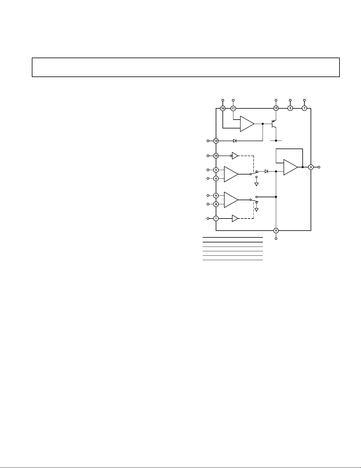
FUNCTIONAL BLOCK DIAGRAM
–IN+IN OUTPUT V+ V–
–
CMP
+
LOGIC
GND
DET
GATED
"
–IN
+IN
–IN
+IN
RST
RST
"g
m
–
AMP
A
+
GATED
"
"g
m
–
AMP
B
+
DET
OPERATIONAL MODE
0
0
0
1
1
PEAK DETECT
1
PEAK HOLD
1
RESET
0
INDETERMINATE
D
The output buffer amplifier features an FET input stage to
reduce droop rate error during lengthy peak hold periods. A bias
current cancellation circuit minimizes droop error at high ambient temperatures.
Through the DET control pin, new peaks may either be detected
or ignored. Detected peaks are presented as positive output
levels. Positive or negative peaks may be detected without
additional active circuits, since Amplifier A can operate as an
inverting or noninverting gain stage.
An uncommitted comparator provides many application options.
Status indication and logic shaping/shifting are typical examples.
V–
OUTPUT
BUFFER
1
–
C
+
PKD01
C
H
SWITCHES SHOWN FOR:
RST = “0,” DET = “0”
OUTPUT
REV. A
Information furnished by Analog Devices is believed to be accurate and
reliable. However, no responsibility is assumed by Analog Devices for its
use, nor for any infringements of patents or other rights of third parties
which may result from its use. No license is granted by implication or
otherwise under any patent or patent rights of Analog Devices.
One Technology Way, P.O. Box 9106, Norwood, MA 02062-9106, U.S.A.
Tel: 781/329-4700 World Wide Web Site: http://www.analog.com
Fax: 781/326-8703 © Analog Devices, Inc., 2001

PKD01–SPECIFICATIONS
ELECTRICAL CHARACTERISTICS
Parameter Symbol Conditions Min Typ Max Min Typ Max Unit
AMPLIFIERS A, B
g
m
Zero-Scale Error V
Input Offset Voltage V
Input Bias Current I
Input Offset Current I
Voltage Gain A
Open-Loop Bandwidth BW A
Common-Mode Rejection Ratio CMRR –10 V ≤ V
Power Supply Rejection Ratio PSRR ± 9 V ≤ V
Input Voltage Range
Slew Rate SR 0.5 0.5 V/µs
Feedthrough Error
Acquisition Time to
0.1% Accuracy
Acquisition Time to t
0.01% Accuracy
1
1
1
1
COMPARATOR
Input Offset Voltage V
Input Bias Current I
Input Offset Current I
Voltage Gain A
Common-Mode Rejection Ratio CMRR –10 V ≤ V
Power Supply Rejection Ratio PSRR ± 9 V ≤ V
Input Voltage Range
1
Low Output Voltage V
“OFF” Output Leakage Current I
Output Short-Circuit Current I
Response Time
2
DIGITAL INPUTS – RST, DET
Logic “1” Input Voltage V
Logic “0” Input Voltage V
Logic “1” Input Current I
Logic “0” Input Current I
MISCELLANEOUS
Droop Rate
3
Output Voltage Swing: V
Amplifier C R
Short-Circuit Current:
Amplifier C I
Switch Aperture Time t
Switch Switching Time ts 50 50 ns
Slew Rate: Amplifier C SR R
Power Supply Current I
NOTES
1
Guaranteed by design.
2
DET = 1, RST = 0.
3
Due to limited production test times, the droop current corresponds to junction temperature (TJ). The droop current vs. time (after power-on) curve clarified this point. Since
most devices (in use) are on for more than 1 second, ADI specifies droop rate for ambient temperature (TA) also. The warmed-up (TA) droop current specification is correlated
to the junction temperature (T
are not subject to production testing.
Specifications subject to change without notice.
) value. ADI has a droop current cancellation circuit that minimizes droop current at high temperature. Ambient (T
J
ZS
OS
B
OS
V
V
CM
t
AQ
AQ
OS
B
OS
V
V
CM
OL
L
SC
t
S
2
H
L
INH
INL
V
DR
OP
SC
AP
SY
(@ VS = ⴞ15 V, CH = 1000 pF, TA = 25ⴗC, unless otherwise noted.)
PKD01A/E PKD01F
24 37mV
23 36mV
80 150 80 250 nA
20 40 20 75 nA
RL = 10 kΩ, VO = ±10 V 18 25 10 25 V/mV
= 1 0.4 0.4 MHz
V
≤ +10 V 8090 7490 dB
CM
≤ ±18 V 8696 7696 dB
S
±10 ±11 ± 10 ±11 V
∆VIN = 20 V, DET = 1, RST = 0 66 80 66 80 dB
20 V Step, A
20 V Step, A
= +1 41 70 41 70 µs
VCL
= +1 45 45 µs
VCL
0.5 1.5 1 3 mV
700 1000 700 1000 nA
75 300 75 300 nA
2kΩ Pull-Up Resistor to 5 V 5 7.5 3.5 7.5 V/mV
≤ +10 V 82 106 82 106 dB
CM
≤ ±18 V 7690 7690 dB
S
±11.5 ±12.5 ±11.5 ±12.5 V
I
≤ 5 mA, Logic GND = 0 V –0.2 +0.15 +0.4 –0.2 +0.15 +0.4 V
SINK
V
= 5 V 2580 2580µA
OUT
V
= 5 V 7 12 45 7 12 45 mA
OUT
5 mV Overdrive, 2 kΩ Pull-Up 150 150 ns
Resistor to 5 V
22V
0.8 0.8 V
VH = 3.5 V 0.02 1 0.02 1 µA
VL = 0.4 V 1.6 10 1.6 10 µA
TJ = 25°C 0.01 0.07 0.01 0.1 mV/ms
T
= 25°C 0.02 0.15 0.03 0.20 mV/ms
A
DET = 1
= 2.5 kΩ±11.5 ±12.5 ± 11 ±12 V
L
7 15 40 7 15 40 mA
75 75 ns
= 2.5 kΩ 2.5 2.5 V/µs
L
No Load 57 69mA
) temperature specifications
A
–2–
REV. A

PKD01
(@ VS = ⴞ15 V, CH = 1000 pF, –55ⴗC ≤ TA ≤ +125ⴗC for PKD01AY, –25ⴗC ≤ TA ≤ +85ⴗC for
ELECTRICAL CHARACTERISTICS
Parameter Symbol Conditions Min Typ Max Min Typ Max Unit
” AMPLIFIERS A, B
“g
m
Zero-Scale Error V
Input Offset Voltage V
Average Input Offset Drift
Input Bias Current I
Input Offset Current I
Voltage Gain A
Common-Mode Rejection Ratio CMRR –10 V ≤ V
Power Supply Rejection Ratio PSRR ± 9 V ≤ V
Input Voltage Range
Slew Rate SR 0.4 0.4 V/µs
Acquisition Time to 0.1% Accuracy1t
COMPARATOR
Input Offset Voltage V
Average Input Offset Drift
Input Bias Current I
Input Offset Current I
Voltage Gain A
Common-Mode Rejection Ratio CMRR –10 V ≤ V
Power Supply Rejection Ratio PSRR ± 9 V ≤ V
Input Voltage Range
Low Output Voltage V
OFF Output Leakage Current I
Output Short-Circuit Current I
Response Time t
DIGITAL INPUTS – RST, DET
Logic “1” Input Voltage V
Logic “0” Input Voltage V
Logic “1” Input Current I
Logic “0” Input Current I
MISCELLANEOUS
Droop Rate
3
Output Voltage Swing
Amplifier C V
Short-Circuit Current
Amplifier C I
Switch Aperture Time t
Slew Rate: Amplifier C SR R
Power Supply Current I
NOTES
1
Guaranteed by design.
2
DET = 1, RST = 0.
3
Due to limited production test times, the droop current corresponds to junction temperature (T
point. Since most devices (in use) are on for more than 1 second, ADI specifies droop rate for ambient temperature (T
specification is correlated to the junction temperature (TJ) value. ADI has a droop current cancellation circuit that minimizes droop current at high temperature.
Ambient (TA) temperature specifications are not subject to production testing.
Specifications subject to change without notice.
1
1
1
1
TCV
B
OS
V
AQ
TCV
B
OS
V
L
SC
S
2
INH
INL
V
SC
AP
SY
PKD01EY, PKD01FY and 0ⴗC ≤ TA ≤ +70ⴗC for PKD01EP, PKD01FP, unless otherwise noted.)
PKD01A/E PKD01F
ZS
OS
OS
47 612mV
36 510mV
–9 –24 –9 –24 µV/°C
160 250 160 500 nA
30 100 30 150 nA
V
CM
OS
RL = 10 kΩ, VO = ±10 V 7.5 9 5 9 V/mV
≤ +10 V 74 82 72 80 dB
CM
≤ ±18 V 80 90 70 90 dB
S
±10 ± 11 ±10 ±11 V
20 V Step, A
= +1 60 60 µs
VCL
2 2.5 2 5 mV
OS
–4 –6 –4 –6 µV/°C
1000 2000 1100 2000 nA
100 600 100 600 nA
V
CM
OL
2 kΩ Pull-Up Resistor to 5 V 4 6.5 2.5 6.5 V/mV
≤ +10 V 80 100 80 92 dB
CM
≤ ±18 V 72 82 72 86 dB
S
±11 ±11 V
I
≤ 5 mA, Logic GND = 0 V –0.2 +0.15 +0.4 –0.2 +0.15 +0.4 V
SINK
V
= 5 V 25 100 100 180 µA
OUT
V
= 5 V 6 10 45 6 10 45 mA
OUT
5 mV Overdrive, 2 kΩ Pull-Up
Resistor to 5 V 200 200 ns
H
L
22 V
0.8 0.8 V
VH = 3.5 V 0.02 1 0.02 1 µA
VL = 0.4 V 2.5 15 2.5 15 µA
DR
TJ = Max Operating Temp. 1.2 10 3 15 mV/ms
T
= Max Operating Temp.
A
DET = 1 2.4 20 6 20 mV/ms
OP
RL = 2.5 kΩ±11 ± 12 ± 10.5 ±12 V
6 12406 1240 mA
75 75 ns
= 2.5 kΩ 22V/µs
L
No Load 5.5 8 6.5 10 mA
). The droop current vs. time (after power-on) curve clarifies this
J
) also. The warmed-up (TA) droop current
A
REV. A
–3–
PKD01
WARNING!
ESD SENSITIVE DEVICE
ABSOLUTE MAXIMUM RATINGS
1, 2
Supply Voltage . . . . . . . . . . . . . . . . . . . . . . . . . . . . . . . . ±18 V
Input Voltage . . . . . . . . . . . . . . . . . . . Equal to Supply Voltage
Logic and Logic Ground
Voltage . . . . . . . . . . . . . . . . . . . . . . Equal to Supply Voltage
Output Short-Circuit Duration . . . . . . . . . . . . . . . . Indefinite
Amplifier A or B Differential Input Voltage . . . . . . . . . . ±24 V
Comparator Differential Input Voltage . . . . . . . . . . . . . ±24 V
Comparator Output Voltage
. . . . . . . . . . . . . . . . . . . . . . Equal to Positive Supply Voltage
Hold Capacitor Short-Circuit Duration . . . . . . . . . . Indefinite
Lead Temperature (Soldering, 60 sec) . . . . . . . . . . . . . 300°C
Storage Temperature Range
PKD01AY, PKD01EY, PKD01FY . . . . . –65°C to +150°C
PKD01EP, PKD01FP . . . . . . . . . . . . . . . –65°C to +125°C
Operating Temperature Range
PKD01AY . . . . . . . . . . . . . . . . . . . . . . . . –55°C to +125°C
PKD01EY, PKD01FY . . . . . . . . . . . . . . . . –25°C to +85°C
PKD01EP, PKD01FP . . . . . . . . . . . . . . . . . . . 0°C to 70°C
Junction Temperature . . . . . . . . . . . . . . . . . –65°C to +150°C
NOTES
1
Absolute maximum ratings apply to both DICE and packaged parts, unless
otherwise noted.
2
Stresses above those listed under Absolute Maximum Ratings may cause permanent damage to the device. This is a stress rating only; functional operation of the
device at these or any other conditions above those listed in the operational
sections of this specification is not implied. Exposure to absolute maximum rating
conditions for extended periods may affect device reliability.
1
Model
ORDERING GUIDE
2
Temperature Package Package
Range Description Option
PKD01AY –55°C to +85°C Cerdip Q-14
PKD01EY –25°C to +85°C Cerdip Q-14
PKD01FY –25°C to +85°C Cerdip Q-14
PKD01EP 0°C to 70°C Plastic DIP N-14
PKD01FP 0°C to 70°C Plastic DIP N-14
NOTES
1
Burn-in is available on commercial and industrial temperature range parts in
cerdip, plastic DIP, and TO-can packages.
2
For devices processed in total compliance to MIL-STD-883, add /883 after
part number. Consult factory for 883 data sheet.
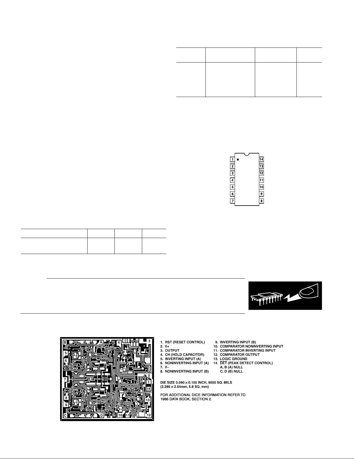
PIN CONFIGURATION
RST
OUTPUT
–IN A
+IN A
V+
PKD01
C
H
V–
DET
LOGIC GND
COMP OUT
–IN C
+IN C
–IN B
+IN B
THERMAL CHARACTERISTICS
Package Type JA*
JC
Unit
14-Lead Hermetic DIP (Y) 99 12 °C/W
14-Lead Plastic DIP (P) 76 33 °C/W
*θJA is specified for worst-case mounting conditions, i.e., θJA is specified for device
in socket for cerdip and PDIP packages.
CAUTION
ESD (electrostatic discharge) sensitive device. Electrostatic charges as high as 4000 V readily
accumulate on the human body and test equipment and can discharge without detection. Although
the PKD01 features proprietary ESD protection circuitry, permanent damage may occur on devices
subjected to high-energy electrostatic discharges. Therefore, proper ESD precautions are
recommended to avoid performance degradation or loss of functionality.
DICE CHARACTERISTICS
–4–
REV. A

PKD01
WAFER TEST LIMITS
(@ VS = ⴞ15 V, CH = 1000 pF, TA = 25ⴗC, unless otherwise noted.)
PKD01N
Parameter Symbol Conditions Limit Unit
“g
” AMPLIFIERS A, B
m
Zero-Scale Error V
Input Offset Voltage V
Input Bias Current I
Input Offset Current I
Voltage Gain A
B
OS
ZS
OS
V
RL = 10 kΩ, VO = ±10 V 10 V/mV min
Common-Mode Rejection Ratio CMRR –10 V ≤ V
Power Supply Rejection Ratio PSRR ±9 V ≤ V
Input Voltage Range
1
V
CM
≤ +10 V 74 dB min
CM
≤ ±18 V 76 dB min
S
7mV max
6mV max
250 nA max
75 nA max
±11.5 V min
Feedthrough Error ∆VIN = 20 V, DET = 1, RST = 0 66 dB min
COMPARATOR
Input Offset Voltage V
Input Bias Current I
Input Offset Current I
Voltage Gain
1
OS
B
OS
A
V
2 kΩ Pull-Up Resistor to 5 V 3.5 V/mV min
Common-Mode Rejection Ratio CMRR –10 V ≤ V
Power Supply Rejection Ratio PSRR ±9 V ≤ V
Input Voltage Range
Low Output Voltage V
1
V
CM
OL
I
≤ 5 mA, Logic GND = 5 V 0.4 V max
SINK
≤ +10 V 82 dB min
CM
≤ ±18 V 76 dB min
S
3mV max
1000 nA max
300 nA max
±11.5 V min
–0.2 V min
“OFF” Output Leakage Current I
Output Short-Circuit Current I
L
SC
V
= 5 V 80 µA max
OUT
V
= 5 V 45 mA min
OUT
7 mA min
DIGITAL INPUTS–RST, DET
Logic “1” Input Voltage V
Logic “0” Input Voltage V
Logic “1” Input Current I
Logic “0” Input Current I
MISCELLANEOUS
Droop Rate
3
Output Voltage Swing Amplifier C V
Short-Circuit Current Amplifier C I
2
2V min
0.8 V max
40 mA max
V
H
L
INH
INL
DR
OP
SC
VH = 3.5 V 1 µA max
VL = 0.4 V 10 µA max
TJ = 25°C, 0.1 mV/ms max
= 25°C 0.20 mV/ms max
T
A
RL = 2.5 kΩ±11 V min
7 mA min
Power Supply Current I
AMPLIFIERS A, B
g
m
Slew Rate SR 0.5 V/µs
Acquisition Time
1
SY
t
A
t
A
No Load 9 mA max
0.1% Accuracy, 20 V Step, A
0.01% Accuracy, 20 V Step, A
= 1 41 µs
VCL
= 1 45 µs
VCL
COMPARATOR
Response Time 5 mV Overdrive, 2 kΩ Pull-Up Resistor to 5 V 150 ns
MISCELLANEOUS
Switch Aperture Time t
Switching Time t
AP
S
75 ns
50 ns
Buffer Slew Rate SR RL = 2.5 kΩ 2.5 V/µs
NOTES
1
Guaranteed by design.
2
DET = 1, RST = 0.
3
Due to limited production test times, the droop current corresponds to junction temperature (T
point. Since most devices (in use) are on for more than 1 second, ADI specifies droop rate for ambient temperature (T
specification is correlated to the junction temperature (TJ) value. ADI has a droop current cancellation circuit that minimizes droop current at high temperature.
Ambient (TA) temperature specifications are not subject to production testing.
). The droop current vs. time (after power-on) curve clarifies this
J
) also. The warmed-up (TA) droop current
A
REV. A
–5–
PKD01
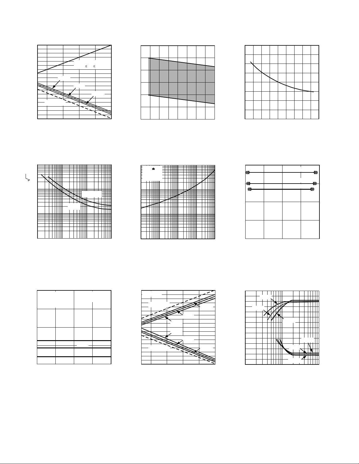
–Typical Performance Characteristics
18
14
10
6
2
–2
–6
–10
INPUT RANGE OF AMPLIFIER – V
V– SUPPLY
–14
–18
46 18
SUPPLY VOLTAGE +V AND –V –V
INPUT + RANGE = V+
–55ⴗC
TA +125ⴗC
–55ⴗC
+25ⴗC
+125ⴗC
91215
TPC 1. A and B Input Range vs.
Supply Voltage
1000
100
10
INPUT NOISE VOLTAGE – nV/ Hz
RS = 10k⍀
RS = 0
6
4
2
0
–2
OFFSET VOLTAGE – mV
–4
–6
–75 –50 125–25 0 25 50 75 100
TEMPERATURE – ⴗC
TPC 2. A and B Amplifiers Offset
Voltage vs. Temperature
100
VS = 15V
T
= 25ⴗC
A
A
= +1
V
10
1
RMS NOISE – V
40
35
30
25
– nA
20
OS
A,B I
15
10
5
0
–25 0 25 75 100 12550
–75 –50 150
TEMPERATURE – ⴗC
TPC 3. A, B IOS vs. Temperature
1.0
0.5
0
ERROR – mV
–0.5
+125ⴗC
+25ⴗC
–55ⴗC
0
110 1k100
FREQUENCY – Hz
TPC 4. Input Spot Noise vs.
Frequency
1.0
POLARITY OF
ERROR MAY BE
POSITIVE OR
NEGATIVE
0.5
0
ERROR – mV
–0.5
–1.0
–10 –50510
V
IN
+125ⴗC
– V
+25ⴗC
–55ⴗC
CH = 1000pF
T
= 25ⴗC
A
TPC 7. Amplifier A Charge Injection Error vs. Input Voltage and
Temperature
0
0.1 1 10010
BANDWIDTH – kHz
1000
TPC 5. Wideband Noise vs.
Bandwidth
18
RL = 10k⍀
14
V+ SUPPLY
10
6
2
–2
–6
OUTPUT SWING – V
–10
V– SUPPLY
–14
–18
46 18
SUPPLY VOLTAGE +V AND –V – V
–55ⴗC
–55ⴗC
91215
+125ⴗC
+25ⴗC
+25ⴗC
+125ⴗC
TPC 8. Output Voltage Swing vs.
Supply Voltage (Dual Supply
Operation)
–1.0
–10 –50 510
– V
V
IN
TPC 6. Amplifier B Charge Injection Error vs. Input Voltage and
Temperature
OUTPUT SWING – Volts
–10.0
–12.5
15
12.5
10.0
7.5
5.0
2.5
0
–2.5
–5.0
–7.5
–15
+25ⴗC
–55ⴗC
+125ⴗC
–55ⴗC
+25ⴗC
+125ⴗC
1.0 10.0
LOAD RESISTOR TO GROUND – k⍀
0.1
TPC 9. Output Voltage vs. Load
Resistance
–6–
REV. A

PKD01
10
0%
100
90
TIME – 20s/DIV
OUTPUT VOLTAGE – 5mV/DIV
TA = 25ⴗC
0V
12
10
8
2mV ERROR
6
4
PK OF SINEWAVE – V
20mV ERROR
2
0
100 1k 1M
FREQUENCY – Hz
200mV ERROR
10k 100k
TPC 10. Output Error vs.
Frequency and Input Voltage
TA = 25ⴗC
100
90
10
0%
OUTPUT VOLTAGE – 5V/DIV
CH = 1000pF
100
90
10
0%
PEAK
OUTPUT
2s10mV
TPC 11. Settling Response
TA = 25ⴗC
100
90
0V
10
0%
OUTPUT VOLTAGE – 5V/DIV
0V
10mV
CH = 1000pF
100
90
10
0%
10mV
3kHz
SINEWAVE
INPUT
TPC 12. Settling Response
2s
DETECTED
PEAK
10V
TIME – 20s/DIV
TPC 13. Large-Signal Inverting
Response
100
90
TA = 25ⴗC
TA = 25ⴗC
10
0%
OUTPUT VOLTAGE – 5mV/DIV
TIME – 20s/DIV
TPC 16. Settling Time for +10 V to
0 V Step Input
TPC 14. Large-Signal Noninverting
Response
90
60
CH = 1000pF
30
GAIN – dB
0V
0
–30
1 10 10M
TPC 17. Small-Signal Open-Loop
Gain/Phase vs. Frequency
TIME – 20s/DIV
GAIN
CH = 1000pF
PHASE
100 1k 10k 100k 1M
FREQUENCY – Hz
TA = 25ⴗC
R
= 10k⍀
L
C
= 30pF
L
C
= 1000pF
H
0
45
90
135
180
TPC 15. Settling Time for –10 V to
0 V Step Input
120
100
80
60
TEST CONDITION:
40
PHASE LAG – Degrees
CH = 1000pF
AMPLIFIER A AND B CONNECTED IN +1 GAIN
20
AMPLIFIER A(B) OFF, INPUT = 20V p-p
AMPLIFIER B(B) ON, INPUT = 0V
CHANNEL-TO-CHANNEL ISOLATION – dB
0
1 10 10M
100 1k 10k 100k 1M
FREQUENCY – Hz
TPC 18. Channel-to-Channel
Isolation vs. Frequency
TA = 25ⴗC
REV. A
–7–

PKD01
HOLD CAPACITANCE – pF
ACQUISITION TIME TO 0.1% ACCURACY – s
500
200
400
300
2000 4000 6000 8000 100000
100
80
60
40
20
0
20V STEP TO 20mV (0.1%)
10V STEP TO 10mV (0.1%)
5V STEP TO 5mV (0.1%)
1V STEP TO 1mV (0.1%)
100
A, AV = +1
B, A
= ⴞ1
80
60
40
OFF ISOLATION – dB
20
0
V
A, AV = –1
1 10 10M
100 1k 10k 100k 1M
FREQUENCY – Hz
TPC 19. Off Isolation vs. Frequency
50
TA = 25ⴗC
= 1000pF
C
H
40
30
20
SETTLING TIME – s
10
0
TO 2mV
51015200
TO 20mV
TO 200mV
INPUT STEP – V
TPC 22. Acquisition Time vs. Input
Voltage Step Size
3
TA = 125ⴗC
= 1000pF
C
H
2
1
DROOP RATE – mV/ms
0
23456789100
1
TIME AFTER POWER APPLIED – Minutes
TPC 20. Droop Rate vs. Time after
Power On
10000
1000
= 1000pF
H
100
10
DROOP RATE (mV/sec), C
1
–100 –50 500
TEMPERATURE – ⴗC
AMBIENT
TEMPERATURE
JUNCTION
TEMPERATURE
100 500
TPC 23. Droop Rate vs. Temperature
TPC 21. Acquisition Time vs.
External Hold Capacitor and
Acquisition Step
5V
RESET
100
90
10
0%
10V
INPUT
10V
PEAK
DETECT
50s
RESET
PEAK
OUTPUT
TPC 24. Acquisition of Step Input
+10V
0V
–10V
+10V
0V
–10V
1V 5mV
1V 5mV
COMPARATOR OUTPUT
COMPARATOR OUTPUT
100
90
5
4
3
2
10
1
OUTPUT VOLTAGE – V
0%
0
TIME – 50ns/DIV
TPC 26. Comparator Output
Response Time (2 k
Resistor, T
= 25°C)
A
–8–
CH = 1000pF
100
90
10
0%
5V
5V
3kHz
SINEWAVE
INPUT
DETECTED
PEAK
RESET
50s
+10V
0V
–10V
TPC 25. Acquisition of Sine
Wave Peak
50ns
50ns
Ω
Pull-Up
1V 5mV
1V 5mV
COMPARATOR OUTPUT
100
90
5
+5
–5
4
0
3
2
10
1
INPUT VOLTAGE – mV
OUTPUT VOLTAGE – V
0%
0
COMPARATOR OUTPUT
TIME – 50ns/DIV
TPC 27. Comparator Output
Response Time (2 k
Resistor, T
= 25°C)
A
50ns
50ns
Ω
Pull-Up
+5
0
–5
INPUT VOLTAGE – mV
REV. A

PKD01
18
14
10
6
2
–2
–6
INPUT LOGIC RANGE – V
–10
–14
–18
–55ⴗC
V–
46
SUPPLY VOLTAGE +V AND –V – V
+VIN V+ FOR
TA +125ⴗC
–55ⴗC
+25ⴗC
+125ⴗC
9121518
TPC 28. Input Logic Range vs.
Supply Voltage
6
+25ⴗC
+125ⴗC
96
SUPPLY CURRENT – mA
–55ⴗC
5
4
31215180
SUPPLY +V AND –V – V
TPC 31. Supply Current vs. Supply
Voltage
18
14
10
6
2
0
–55ⴗC
–2
–6
–10
–14
INPUT RANGE OF LOGIC GROUND – V
–18
46 9 12 1815
SUPPLY VOLTAGE +V AND –V – V
V+
+125ⴗC
+25ⴗC
ACCEPTABLE GROUND PIN
POTENTIAL IS BETWEEN
SLIDE LINES.
+25ⴗC
+125ⴗC
V–
TPC 29. Input Range of Logic
Ground vs. Supply Voltage
100
REJECTION RATIO – dB
80
60
40
20
0
POSITIVE SUPPLY
(+15V +1V SIN T)
NEGATIVE SUPPLY
(–15V +1V SIN )
CHANNEL A = 1
CHANNEL B = 0
10 100 1M
1k 10k 100k
FREQUENCY – Hz
TA = 25ⴗC
= 0V
V
IN
= 1000pF
C
H
TPC 32. Hold Mode Power Supply
Rejection vs. Frequency
1
LOGIC 1
0
–1
LOGIC CURRENT – A
–2
–3
+125ⴗC
LOGIC 0
–2 –15
01234
LOGIC INPUT VOLTAGE – V
–55ⴗC
+25ⴗC
LOGIC GROUND = 0V
TPC 30. Logic Input Current vs.
Logic Input Voltage
3
VS = ⴞ15V
= 25ⴗC
T
A
2
1
0
–1
INPUT BIAS CURRENT (EITHER INPUT) – A
–15 –10 15
INPUT CURRENT
MUST BE LIMITED
TO LESS THAN 1mA
OTHER
INPUT
AT –10V
–50 510
INPUT VOLTAGE – V
OTHER
INPUT
AT 0V
OTHER
INPUT
AT +10V
TPC 33. Comparator Input Bias
Current vs. Differential Input Voltage
3
2
1
0
–1
OFFSET VOLTAGE – mV
–2
–3
–75 –50 125–25 0 25 50 75 100
TEMPERATURE – ⴗC
TPC 34. Comparator Offset Voltage
vs. Temperature
REV. A
110
100
90
– nA
OS
80
70
COMPARATOR I
60
50
–25 0 25 75 100 12550
–75 –50 150
TEMPERATURE – ⴗC
TPC 35. Comparator IOS vs.
Temperature
–9–
1200
1000
– nA
B
800
600
COMPARATOR I
400
200
–25 0 25 75 100 12550
–75 –50 150
TEMPERATURE – ⴗC
TPC 36. Comparator IB vs.
Temperature

PKD01
18
14
10
6
2
–55ⴗC
–2
–6
–10
–14
OUTPUT RANGE OF COMPARATOR – V
–18
46 9121518
SUPPLY VOLTAGE +V AND –V – V
V+
+125ⴗC
+25ⴗC
+25ⴗC
+125ⴗC
V–
TPC 37. Output Swing of Com parator vs. Supply Voltage
1.0
0.8
DC
0.6
0.4
0.2
0
– VOLTAGE OUTPUT – V
O
V
–0.2
014
IO – OUTPUT SINK CURRENT – mA
+125ⴗC
+25ⴗC
–55ⴗC
42 6 10 128
5
PULL-UP
RESISTOR = 2k⍀
4
3
2
TA = –55ⴗC
OUTPUT VOLTAGE – V
1
0
+5
0
–5
INPUT VOLTAGE – mV
–50 300
TPC 38. Comparator Response
Time vs. Temperature
5
4
3
TA = –55ⴗC
2
OUTPUT VOLTAGE – V
1
0
+5
0
–5
INPUT VOLTAGE – mV
–50 300
TA = +25ⴗC
500 100 200 250150
TA = +25ⴗC
500 100 200 250150
TIME – ns
TIME – ns
TA = +125ⴗC
PULL-UP
RESISTOR = 2k⍀
TA = +125ⴗC
6
INVERTING INPUT = V
NONINVERTING INPUT = 0V
5
4
3
RL = 2k⍀
TO 5V
2
OUTPUT VOLTAGE – V
1
0
–1.5 2.0
–0.5–1.0 0 1.0 1.50.5
INPUT VOLTAGE – mV
IN
R
= 1k⍀
L
TO 5V
VS = ⴞ15V
= 25ⴗC
T
A
TPC 39. Comparator Transfer
Characteristic
TPC 40. Comparator Output
Voltage vs. Output Current and
Temperature
TPC 41. Comparator Response
Time vs. Temperature
–10–
REV. A

PKD01
THEORY OF OPERATION
The typical peak detector uses voltage amplifiers and a diode or
an emitter follower to charge the hold capacitor, C
ionally (see Figure 1). The output impedance of A plus D
dynamic impedance, r
, make up the resistance which deter-
d
, indirect-
H
’s
1
mines the feedback loop pole. The dynamic impedance is
kT
r
=
d
The pole moves toward the origin of the S plane as I
, where Id is the capacitor charging current.
qI
d
goes to
d
zero. The pole movement in itself will not significantly lengthen
the acquisition time since the pole is enclosed in the system
feedback loop.
V
(A) = VIN (A) ⴛ AV (A)
OUT
A
V
V
IN
INPUT
OUT
R
OUT
+
D
1
V
r
d
C
H
C
H
OUTPUT
Figure 1. Conventional Voltage Amplifier Peak Detector
When the moving pole is considered with the typical frequency
compensation of voltage amplifiers however, there is a loop stability
problem. The necessary compensation can increase the required
acquisition time. ADI’s approach replaces the input voltage amplifier with a transconductance amplifier (see Figure 2).
The PKD01 transfer function can be reduced to:
V
OUT
=
V
IN
++
1
where: gm ⬇ 1 µA/mV, R
1
sC
H
ggR
mm
⬇ 20 MΩ.
OUT
1
OUT
1
≈
sC
H
+
1
g
m
The diode in series with A’s output (see Figure 2) has no effect
because it is a resistance in series with a current source. In
addition to simplifying the system compensation, the input
transconductance amplifier output current is switched by current steering. The steered output is clamped to reduce and match
any charge injection.
I
(A) = VIN (A) ⴛ gm (A)
OUT
A
I
V
IN
INPUT
OUT
R
OUT
D
1
V
H
C
C
H
OUTPUT
V
OUT
Figure 2. Transconductance Amplifier Peak Detector
Figure 3 shows a simplified schematic of the reset gm amplifier,
B. In the track mode, Q
OFF. A current of 2I passes through D
passes through Q
1
can absorb only 3I, thus the current passing through D
and Q4 are ON and Q2 and Q3 are
1
, I is summed at B and
1
, and is summed with gmVIN. The current sink
can
2
only be: 2K – g
node then, is g
Q
and Q3 are ON while Q1 and Q4 are OFF. The net current
2
into the top of D
bottom of D
thus, D
is pulled up with a current I until D4 turns ON,
2
and D2 are reverse biased by <0.6 V, and charge injec-
1
. The net current into the hold capacitor
m VIN
mVIN [IH
= 2I – (2I – gmVIN)]. In the hold mode,
is –I until D3 turns ON. With Q1 OFF, the
1
tion is independent of input level.
The monolithic layout results in points A and B having equal
nodal capacitance. In addition, matched diodes D
and D2 have
1
equal diffusion capacitance. When the transconductance amplifier outputs are switched open, points A and B are ramped
equally, but in opposite phase. Diode clamps D
and D4 cause
3
the swings to have equal amplitudes. The net charge injection
(voltage change) at node C is therefore zero.
V+
I
2I
A
D
1
C
D
2
B
Q
Q
2
1
gm V
V
IN
IN
3I
D
3
C
D
4
C
H
6
Q
Q
4
3
3I
A
B
A > B = PEAK DETECT
V–
A < B = PEAK HOLD
LOGIC
CONTROL
Figure 3. Transconductance Amplifier with Low Glitch
Current Switch
The peak transconductance amplifier, A is shown in Figure 4.
Unidirectional hold capacitor charging requires diode D
to be
1
connected in series with the output. Upon entering the peak
hold mode D
is reverse-biased. The voltage clamp limits charge
1
injection to approximately 1 pC and the hold step to 0.6 mV.
Minimizing acquisition time dictates a small C
capacitance. A
H
1000 pF value was selected. Droop rate was also minimized by
providing the output buffer with an FET input stage. A current cancellation circuit further reduces droop current and
minimizes the gate current’s tendency to double for every 10°
temperature change.
V+
I
2I
D
2
Q
Q
2
1
gm V
V
IN
IN
3I
D
3
D
1
r
D
d
4
6
Q
Q
3
3I
C
C
H
4
A > B = PEAK DETECT
V–
A < B = PEAK HOLD
A
B
LOGIC
CONTROL
Figure 4. Peak Detecting Transconductance Amplifier
with Switched Output
REV. A
–11–

PKD01
APPLICATIONS INFORMATION
Optional Offset Voltage Adjustment
Offset voltage is the primary zero scale error component since a
variable voltage clamp limits voltage excursions at D
’s anode
1
and reduces charge injection. The PKD01 circuit gain and operational mode (positive or negative peak detection) determine the
applicable null circuit. Figures 5 through 8 are suggested circuits.
Each circuit also corrects amplifier C offset voltage error.
100k⍀
+
V
S
0.1F
VIN+
NOTES:
1. NULL RANGE = ⴞV
2. DISCONNECT RC FROM CH AFTER AMPLIFIER A ADJUSTMENT.
3. REPEAT NULL CIRCUIT FOR RESET BUFFER AMPLIFIER B IF REQUIRED.
R
A
VS–
R2
2M⍀
DET
R1
1k⍀
, RB AND RC NOT NECESSARY FOR AMPLIFIER B ADJUSTMENT.
A
B
RST
R1
(
)
S
R2
R1
1k⍀
D
1
C
R
2M⍀
–15V
C
C
H
1000pF
PKD01
V
OUT
R
A
200k⍀
R
B
1k⍀
Figure 5. VOS Null Circuit for Unity Gain Positive Peak
Detector
R2 = R3 + R4
DET
IN
VS–
V
R1
R1
+
R3
R5
20k⍀
R4
0.1F
+
S
20⍀
R5
(
S
R4
)( )
R1 + R3
VIN–
V
25k⍀
NOTES:
1. NULL RANGE = ⴞV
2. DISCONNECT RC FROM CH AFTER AMPLIFIER A ADJUSTMENT.
3. REPEAT NULL CIRCUIT FOR RESET BUFFER AMPLIFIER B IF REQUIRED.
A
B
RST
R1
D
1
R
2M⍀
V
OUT
–15V
R
A
C
200k⍀
R
B
1k⍀
C
H
1000pF
C
PKD01
Figure 6. VOS Null Circuit for Differential Peak Detector
A. Nulling Gated Output g
Amplifier A. Diode D1 must
m
be conducting to close the feedback circuit during amplifier A
adjustment. Resistor network RA – RC cause D1 to conduct
V
OS
slightly. With DET = 0 and V
output. Adjust the null potentiometer until V
adjustment, disconnect R
B. Nulling Gated g
input to V
= 0 V and monitor the PKD01 output. Set DET =
IN
Amplifier B. Set Amplifier B signal
m
1, RST = 1 and adjust the null potentiometer for V
= 0 V, monitor the PKD01
IN
from CH.
C
OUT
= 0 V. After
= 0 V.
OUT
The circuit gain—inverting or noninverting—will determine which
null circuit illustrated in Figures 5 through 8 is applicable.
V
IN
VS–
25k⍀
V
NOTES:
1. NULL RANGE = ⴞV
2. DISCONNECT RC FROM CH AFTER AMPLIFIER A ADJUSTMENT.
3. REPEAT NULL CIRCUIT FOR RESET BUFFER AMPLIFIER B IF REQUIRED.
R1
DET
R3
20k⍀
R4
0.1F
+
S
20⍀
S
A
B
RST
R4
(
)
R3
R2
D
1
R
2M⍀
V
OUT
–15V
R
A
C
200k⍀
R
B
1k⍀
C
H
1000pF
C
PKD01
Figure 7. VOS Null Circuit for Negative Peak Detector
VS–
25k⍀
V
V
IN
NOTES:
1. NULL RANGE = ⴞV
2. DISCONNECT RC FROM CH AFTER AMPLIFIER A ADJUSTMENT.
3. REPEAT NULL CIRCUIT FOR RESET BUFFER AMPLIFIER B IF REQUIRED.
R5
R1
20k⍀
R3
0.1F
R4 =
20⍀
R4
R2 R1
R1 + R2
S
+
S
DET
A
B
RST
R3
(
)
R5
R2
D
1
C
H
1000pF
GAIN = 1 +
C
PKD01
R
2M⍀
C
R1 + R3
–15V
R2
V
OUT
R
A
200k⍀
R
B
1k⍀
Figure 8. VOS Null Circuit for Positive Peak Detector with
Gain
–12–
REV. A

PKD01
PEAK HOLD CAPACITOR RECOMMENDATIONS
The hold capacitor (CH) serves as the peak memory element
and compensating capacitor. Stable operation requires a minimum value of 1000 pF. Larger capacitors may be used to lower
droop rate errors, but acquisition time will increase.
Zero scale error is internally trimmed for C
C
values will cause a zero scale shift which can be approxi-
H
= 1000 pF. Other
H
mated with the following equation.
pC
×
110
∆VmV
()
ZS
=
()
CnF
()
H
mV
−
063.
The peak hold capacitor should have very high insulation resistance and low dielectric absorption. For temperatures below
85°C, a polystyrene capacitor is recommended, while a Teflon
capacitor is recommended for high temperature environments.
CAPACITOR GUARDING AND GROUND LAYOUT
Ground planes are recommended to minimize ground path
resistance. Separate analog and digital grounds should be used.
The two ground systems are tied together only at the common
system ground. This avoids digital currents returning to the
system ground through the analog ground path.
PKD01
1
2
3
4
5
6
7
C
H
REPEAT ON
“COMPONENT SIDE”
OF PC BOARD IF POSSIBLE
14
13
12
11
10
9
8
BOTTOM VIEW
Figure 9. CH Terminal (Pin 4) Guarding. See Text.
The CH terminal (Pin 4) is a high impedance point. To minimize
gain errors and maintain the PKD01’s inherently low droop rate,
guarding Pin 4 as shown in Figure 9 is recommended.
COMPARATOR
The comparator output high level (VOH) is set by external resistors. It is possible to optimize noise immunity while interfacing
to all standard logic families—TTL, DTL, and CMOS. Figure
10 shows the comparator output with external level-setting
resistors. Table I gives typical R1 and R2 values for common
circuit conditions.
The maximum comparator high output voltage (V
) should be
OH
limited to:
V
(maximum) < V+ –2.0 V
OH
With the comparator in the low state (V
will be required to sink a current approximately equal to V
), the output stage
OL
C
/R1.
COMPARATOR
INPUT
CMP
INVERTING
COMPARATOR
INPUT
PKD01
DIGITAL
GND
V–
V
R1 = R2
C
R1
R2
V
(
V
V
OH
C
–1
)
OH
Figure 10. Comparator Output with External Level-Setting
Resistors
Table I.
V
VCV
OH
R1 R2
R
1 ≈
I
C
SINK
5 3.5 2.7 kΩ 6.2 kΩ
5 5.0 2.7 kΩ ⬁
15 3.5 4.7 kΩ 1.5 kΩ
15 5.0 4.7 kΩ 2.4 kΩ
15 7.5 7.5 kΩ 7.5 kΩ
15 10.0 7.5 kΩ 15 kΩ
R
2
V
1
V
C
1≈−
OH
PEAK DETECTOR LOGIC CONTROL (RST, DET)
The transconductance amplifier outputs are controlled by the
digital logic signals RST and DET. The PKD01 operational
mode is selected by steering the current (I
) through Q1 and Q2,
1
thus providing high-speed switching and a predictable logic
threshold. The logic threshold voltage is 1.4 V when digital
ground is at zero volts.
Other threshold voltages (V
) may be selected by applying
TH
the formula:
V
≈ 1.4 V + Digital Ground Potential.
TH
For proper operation, digital ground must always be at least
3.5 V below the positive supply and 2.5 V above the negative
supply. The RST or DET signal must always be at least 2.8 V
above the negative supply.
Operating the digital ground at other than zero volts does influence
the comparator output low voltage. The V
level is referenced
OL
to digital ground and will follow any changes in digital ground
potential:
V
≈ 0.2 V + Digital Ground Potential.
OL
REV. A
–13–

PKD01
DET OR RST
I
1
Q
Q
CURRENT TO
CONTROL MODES
2
1
I
2
D
Q
3
V–
Figure 11. Logic Control
Typical Circuit Configurations
INPUT
OUTPUT
V+
DIGITAL
GROUND
+10V
0V
+10V
0V
DET/RST
INPUT
RESET
VO LTAG E
+18V
56k⍀
5%
1
2
3
PKD01
4
5
6
7
36k⍀
5%
–18V
18k⍀
5%
Figure 12. Burn-In Circuit
V+ V–
D
1
A
PKD01
B
C
A GAIN = +1
B GAIN = +1
14
13
12
11
10
9
8
OUTPUT
INPUT
OUTPUT
TIME – 50s/DIV
TIME – 50s/DIV
Figure 13. Unity Gain Positive Peak Detector
DET
10k⍀
+5V
0V
–2V
+10V
0V
–4V
–10V
INPUT
(GAIN = +2)
VOLTAGE = +1V
(RESETS TO –4V)
40.2k⍀
RESET
5.1k⍀
5%
1%
10k⍀
1%
10k⍀
8.2k⍀
RST
1%
5%
5%
Figure 14. Positive Peak Detector with Gain
A
PKD01
B
C
H
1000pF
V+ V–
D
1
C
A GAIN = +2
B GAIN = –4
C
H
1000pF
OUTPUT
–14–
REV. A

PKD01
INPUT
OUTPUT
INPUT
OUTPUT
TIME – 50s/DIV
DET/RST
20k⍀
10k⍀
1%
30.1k⍀
RESET
1%
1%
10k⍀
1%
8.2k⍀
5%
7.5k⍀
5%
RST
+2V
0V
–5V
+10V
0V
–4V
–10V
INPUT
(GAIN = –2)
VOLTAGE = –1V
(RESETS TO –4V)
Figure 15. Negative Peak Detector with Gain
DET
10k⍀
1%
10k⍀
5%
0V
–10V
+10V
0V
V
IN
10k⍀
1%
RESET
VO LTAG E
A
PKD01
B
A
PKD01
B
V+ V–
D
1
V+ V–
D
1
C
A GAIN = –2
B GAIN = +4
C
H
1000pF
C
A GAIN = –1
B GAIN = +1
OUTPUT
OUTPUT
INPUT
RESET
VO LTAG E
R3
R4
R1
TIME – 50s/DIV
A
B
Figure 16. Unity Gain Negative Peak Detector
R2
OUTPUT
INPUT AMPLIFIER GAIN
RESET AMPLIFIER GAIN
R3 = R4 =
1
1R11
+
R2
= 1 +
R1
R2
PKD01
C
H
1000pF
C
Figure 17. Alternate Gain Configuration
C
H
1000pF
IF BOTH INPUT SIGNAL (AMPLIFIER A INPUT) AND THE RESET
VOLTAGE (AMPLIFIER B INPUT) HAVE THE SAME POSITIVE
VOLTAGE GAIN, THE GAIN CAN BE SET BY A SINGLE VOLTAGE
DIVIDER FOR BOTH INPUT AMPLIFIERS.
NOTE:
R1, R2, R3 AND R4 > 5k
⍀
REV. A
–15–

PKD01
V
PEAK DETECTOR
INPUT
IN
POS/NEG
R
VPK+
PKD01
POSITIVE
PEAK
DETECTOR
V
IN
PKD01
–
V
PK
NEGATIVE
PEAK
DETECTOR
VPK+
VPK–
10k⍀
10k⍀
10k⍀
OP27
VPK– + VPK+
10k⍀
V
OUT
Figure 18. Peak-to-Peak Detector
+15V
10.5k⍀
S2
SW-02
S1
S3
S4
R
+15V –15V
PKD01
1000pF
C
H
POLYSTYRENE
OUTPUT
PEAK DETECTOR
RESET
Figure 19. Logic Selectable Positive or Negative Peak Detector
PORT 0
PROCESSOR
PORT 1
0
1
2
3
4
5
6
7
0
1
2
3
4
5
6
7
BIT 1
BIT 10
–15V
DAC10
NOTES:
1. DEVICE IS RESET TO 0 VOLTS.
2. DETECTED PEAKS ARE PRESENTED AS POSITIVE OUTPUT LEVELS.
3. R = 10k⍀.
5V
2.7k⍀
RESET
VO LTAG E
INPUT
SIGNAL
DET
RST
CMP
D
1
A
B
C
PKD01
C
H
R
R
Figure 20. Peak Reading A/D Converter
–16–
REV. A

V
V
RS
V
RS
V
RS
VRS4
A1
A2
A3
A4
PK DET/RST
IN
1
2
3
–15V +15V
SW-201
5V
A
B
ANALOG
–15V+15V
GND
C
PKD01
LOGIC
GND
V
OUT
INPUT
PEAK
DETECT
OUTPUT
NOTES:
RESET VOLTAGE = –1.0V
TRACE 1 = 2V/DIV
TRACE 2 = 5V/DIV
TRACE 3 = 2V/DIV
Figure 21. Positive Peak Detector with Selectable Reset Voltage
PKD01
RESET
1ms2V
AMPLITUDE
SELECTION
LOGIC
RAMP
AMPLITUDE
DET
D
A0 A1 A2
CH1
CH2
CH3
CH4
MUX-08
CH5
CH6
CH7
CH8
RAMP
AMPLITUDE
RAMP
START
PULSE
0
RAMP START
PULSE
SLOPE =
~0.5V/s
NOTES:
1. NEGATIVE SLOPE OF RAMP IS SET BY DAC08 OUTPUT CURRENT.
2. DAC08 IS A DIGITALLY CONTROLLED CURRENT GENERATOR.
THE MAXIMUM FULL-SCALE CURRENT MUST BE LESS THAN 0.5mA.
1
A
B
RST
I
0
C
~0.5V/s
C
PKD01
I
C
H
I
SLOPE =
1
C
Figure 22. Programmable Low Frequency Ramp Generator
BUFFERED
RAMP
OUTPUT
RAMP SLOPE
SELECTION
B1 B8
DAC08
R > 20k⍀
15V
REF-01
REV. A
–17–

PKD01
OUTLINE DIMENSIONS
Dimensions shown in inches and (mm).
14-Lead Plastic DIP (PDIP)
0.795 (20.19)
0.725 (18.42)
14
17
PIN 1
0.210 (5.33)
MAX
0.160 (4.06)
0.115 (2.93)
0.005 (0.13) MIN 0.098 (2.49) MAX
0.200 (5.08)
0.200 (5.08)
0.125 (3.18)
0.100 (2.54)
0.022 (0.558)
0.014 (0.356)
14
PIN 1
17
0.100 (2.54) BSC
0.785 (19.94) MAX
MAX
0.023 (0.58)
0.014 (0.36)
(N-14)
8
0.280 (7.11)
0.240 (6.10)
0.070 (1.77)
0.045 (1.15)
0.060 (1.52)
0.015 (0.38)
SEATING
PLANE
BSC
14-Lead Cerdip
(Q-14)
8
0.310 (7.87)
0.220 (5.59)
0.060 (1.52)
0.015 (0.38)
0.070 (1.78)
0.030 (0.76)
SEATING
PLANE
0.130
(3.30)
MIN
0.150
(3.81)
MIN
0.325 (8.25)
0.300 (7.62)
0.015 (0.381)
0.008 (0.204)
0.320 (8.13)
0.290 (7.37)
15°
0°
0.195 (4.95)
0.115 (2.93)
0.015 (0.38)
0.008 (0.20)
C00481-0-2/01 (rev. A)
–18–
PRINTED IN U.S.A.
REV. A
 Loading...