

–
查询OP11A供应商
Quad Matched
a
FEATURES
Guaranteed V
Guaranteed Matched CMRR: 94 dB Min
Guaranteed Matched VOS: 750 V Max
LM148/LM348 Direct Replacement
Low Noise
Silicon-Nitride Passivation
Internal Frequency Compensation
Low Crossover Distortion
Continuous Short-Circuit Protection
Low Input Bias Current
GENERAL DESCRIPTION
The OP11 provides four matched 741-type operational amplifiers
in a single 14-lead DIP package. The OP11 is pin compatible
with the LM148, LM348, RM4156, RM4158, and HA4741
amplifiers. The amplifier is matched for common-mode rejection
ratio and offset voltage which is very important in designing
instrumentation amplifiers. In addition, the amplifier is designed
to have equal positive-going and negative-going slew rates. This
is an important consideration for good audio system performance.
The OP11 is ideal for use in designs requiring minimum space
and cost while maintaining performance.
: 500 V Max
OS
741-Type Operational Amplifiers
OP11
PIN CONFIGURATIONS
14-Lead Epoxy DIP
(P Suffix)
1
OUT A
2
–IN A
3
+IN A
4
V+
5
+IN B
6
–IN B
7
OUT B
14-Lead Hermetic DIP
(Y Suffix)
1
OUT A
2
–IN A
3
+IN A
4
V+
5
+IN B
6
–IN B
7
OUT B
14
OUT D
13
–IN D
12
+IN D
11
V–
10
+IN C
9
–IN C
8
OUT C
14
OUT D
13
–IN D
12
+IN D
11
V–
10
+IN C
9
–IN C
8
OUT C
V+
IN
+IN
OUTPUT
V–
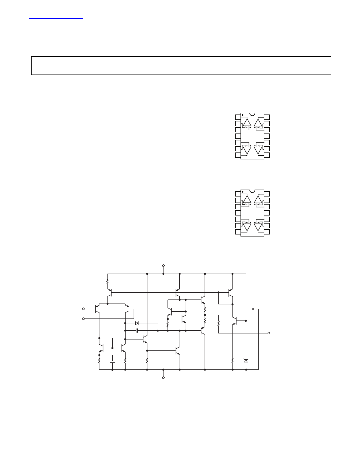
Figure 1. Simplified Schematic
REV. A
Information furnished by Analog Devices is believed to be accurate and
reliable. However, no responsibility is assumed by Analog Devices for its
use, nor for any infringements of patents or other rights of third parties that
may result from its use. No license is granted by implication or otherwise
under any patent or patent rights of Analog Devices.
One Technology Way, P.O. Box 9106, Norwood, MA 02062-9106, U.S.A.
Tel: 781/329-4700 www.analog.com
Fax: 781/326-8703 © Analog Devices, Inc., 2002

OP11–SPECIFICATIONS
ELECTRICAL CHARACTERISTICS
(@ VS = 15 V, TA = 25C, unless otherwise noted)
OP11A/OP11E OP11F OP11G
Parameter Symbol Conditions Min Typ Max Min Typ Max Min Typ Max Unit
Input Offset Voltage V
Input Offset Current I
Input Bias Current I
OS
OS
B
RS = 10 kW 0.3 0.5 0.6 2.5 1.2 5.0 mV
5.5 20 25 50 75 200 nA
180 300 300 500 300 500 nA
Input Resistance
Differential Mode1R
IN
0.17 0.29 0.1 0.17 0.1 0.17 MW
Input Voltage Range IVR ±12 ±13 ±12 ± 13 ±12 ±13 V
Common-Mode CMRR
Rejection Ratio VCM = ±12 V, RS = 10 kW 100 120 100 120 70 100 dB
Power Supply VS = ±5 V to ±15 V,
Rejection Ratio PSRR RS £ 10 kW 432 432 10 100 mV/V
Output Voltage
Swing V
O
RL = 2 kW±11 ±13 ±11 ± 13 ±11 ±13 V
Large-Signal
Voltage Gain A
Power Consumption2P
VO
d
RL £ 2 kW, VO = ±10 V 100 650 100 650 50 500 V/mV
VO = 0 V 105 180 123 180 210 340 mW
Input Noise Voltage en p-p 0.1 Hz to 10 Hz 0.7 0.7 0.7 mV p-p
Input Noise Voltage e
n
fO = 10 Hz 18 18 18 nV/÷Hz
Density fO = 100 Hz 14 14 14 nV/÷Hz
fO = 1 MHz 12 12 12 nV/÷Hz
Input Noise Current In p-p 0.1 Hz to 10 Hz 17 17 17 pA p-p
Input Noise Current I
n
fO = 10 Hz 1.8 1.8 1.8 pA/÷Hz
Density fO = 100 Hz 1.5 1.5 1.5 pA/÷Hz
fO = 1 MHz 1.2 1.2 1.2 pA/÷Hz
Channel Separation CS 100 130 100 130 130 dB
Slew Rate
Large Signal
Closed-Loop
Rise Time
Overshoot
NOTES
1
Guaranteed by input bias current.
2
Total dissipation for all four amplifiers in package.
3
Sample tested.
4
Guaranteed by rise time.
Specifications subject to change without notice
2
Bandwidth
Bandwidth
3
3
SR 0.7 1.0 0.7 1.0 0.7 1.0 V/ms
3
4
BW A
t
f
VO = 20 V p-p 11 16 11 16 11 16 kHz
= 1 2.4 3.0 2.4 3.0 2.4 3.0 MHz
VCL
AV = 1, VIN = 50 mV 110 145 110 145 110 145 ns
OS 15 25 15 25 15 25 %
–2–
REV. A

OP11
ELECTRICAL CHARACTERISTICS
(@ VS = 15 V, 55C £ TA £ 125C for OP11A, 0C £ T
otherwise noted)
£ 70C for OP11E, unless
A
OP11A OP11E
Parameter Symbol Conditions Min Typ Max Min Typ Max Unit
Input Offset Voltage V
Average Input Offset Voltage Drift
1
Input Offset Current I
Average Input Offset Current Drift
1
Input Bias Current I
OS
TCV
OS
TCI
B
RS £ 10 kW 0.4 1.0 0.4 0.8 mV
RS £ 10 kW 2.0 10 2.0 10 mV/∞C
OS
20 40 14 30 nA
OS
0.1 0.3 0.1 0.3 nA/∞C
200 375 200 350 nA
Input Voltage Range IVR ±12 ±13 ±12 ±13 V
Common-Mode Rejection Ratio CMRR V
= ±12 V,
CM
RS £ 10 kW 100 120 100 120 dB
Power Supply Rejection Ratio PSRR VS = ±5 V to ±15 V,
RS £ 10 kW 432 4 32mV/V
Large-Signal Voltage Gain A
VO
RL ≥ 2 kW,
VO = ±10 V 50 250 50 250 V/mV
Output Voltage Swing V
Power Consumption
NOTES
1
Guaranteed but not tested.
2
Total dissipation for all four amplifiers in package.
Specifications subject to change without notice
2
O
P
d
RL ≥ 2 kW±11 ±13 ±11 ±13 V
VO = 0 V 115 200 115 200 mW
ELECTRICAL CHARACTERISTICS
(@ VS = 15 V, 40C £ T
£ +85C, R
A
£ 100 , unless otherwise noted)
S
OP11F OP11G
Parameter Symbol Conditions Min Typ Max Min Typ Max Unit
Input Offset Voltage V
OS
Average Input Offset Voltage Drift TCV
Input Offset Current I
Average Input Offset Current Drift
1
Input Bias Current I
OS
TCI
B
RS £ 10 kW 0.8 3.0 1.5 6 .0 mV
RS £ 10 kW 4.0 15 4.0 mV/∞C
OS
40 60 250 300 nA
OS
0.3 0.6 0.3 0.6 nA/∞C
400 550 400 800 nA
Input Voltage Range IVR ±12 ±13 ±12 ±13 V
Common-Mode Rejection Ratio CMRR V
= ±12 V,
CM
RS £ 10 kW 100 120 70 100 dB
Power Supply Rejection Ratio PSRR V
= ±5 V to ±15 V,
S
RS £ 10 kW 432 10100 mV/V
Large-Signal Voltage Gain A
VO
RL ≥ 2 kW,
VO = ±10 V 50 250 25 100 V/mV
Output Voltage Swing V
Power Consumption
NOTES
1
Guaranteed but not tested.
2
Total dissipation for all four amplifiers in package.
Specifications subject to change without notice
2
O
P
d
RL ≥ 2 kW±11 ±13 ±11 ±13 V
VO = 0 V 115 200 250 400 mW
REV. A
–3–

OP11
WARNING!
ESD SENSITIVE DEVICE
ABSOLUTE MAXIMUM RATINGS*
Supply Voltage (VS) . . . . . . . . . . . . . . . . . . . . . . . . . . . . ±22 V
Input Voltage* . . . . . . . . . . . . . . . . . . . . . . . . . Supply Voltage
Differential Input Voltage . . . . . . . . . . . . . . . . . . . . . . . ±30 V
Output Short-Circuit Duration . . . . . . . . . . . . . . . Continuous
(One Amp Only)
Storage Temperature Range
Y Package . . . . . . . . . . . . . . . . . . . . . . . . –65∞C to +150∞C
P Package . . . . . . . . . . . . . . . . . . . . . . . . . –65∞C to +125∞C
Lead Temperature Range (Soldering, 60 sec) . . . . . . . . 300∞C
Operating Temperature Range
OP11A . . . . . . . . . . . . . . . . . . . . . . . . . . . –55∞C to +125∞C
OP11E . . . . . . . . . . . . . . . . . . . . . . . . . . . . . . . 0∞C to 70∞C
OP11F, OP11G . . . . . . . . . . . . . . . . . . . . . –40∞C to +85∞C
*Absolute maximum ratings apply to both DICE and packaged parts, unless
otherwise noted.
Package Type JA*
JC
Unit
14-Lead Plastic DIP (P) 83 39 ∞C/W
14-Lead Hermetic DIP (Y) 108 15 ∞C/W
*qJA is specified for worst-case conditions, i.e., q
socket for CERDIP and P-DIP packages.
ORDERING GUIDE
is specified for device in
JA
Temperature Package Package
Model Range Description Option
OP11AY* –40∞C to +125∞C 14-Lead CERDIP Y-14
OP11EP –40∞C to +125∞C 14-Lead Epoxy DIP P-14
OP11EY* 0∞C to 85∞C 14-Lead CERDIP Y-14
OP11FP* –40∞C to 85∞C 14-Lead Epoxy DIP P-14
OP11GP –40∞C to 85∞C 14-Lead Epoxy DIP P-14
*Not for new designs. Obsolete April 2002.
For Military processed devices, please refer to the Standard
Microcircuit Drawing (SMD) available at
www.dscc.dla.mil/programs/milspec/default.asp
SMD Part Number ADI Equivalent
5962-89801012A OP11ARCMDA
5962-8980101CA OP11AYMDA
MATCHING CHARACTERISTICS
(@ VS = 15 V, TA = 25C, RS £ 100 , unless otherwise noted)
OP11A, OP11E OP11F
Parameter Symbol Conditions Min Typ Max Min Typ Max Unit
Input Offset Voltage Match DV
OS
Common-Mode Rejection Ratio Match DCMRR V
= ±12 V 1 20 1 20 mV/V
CM
0.5 0.75 0.6 2.0 mV
VCM = ±12 V 94 120 94 120 dB
Specifications subject to change without notice
MATCHING CHARACTERISTICS
(@ VS = 15 V, 55C £ T
+85C for OP11F, RS £ 100 , unless otherwise noted)
£ +125C for OP11A, 0C £ TA £ 70C for OP11E, 40C £ TA £
A
OP11A, OP11E OP11F
Parameter Symbol Conditions Min Typ Max Min Typ Max Unit
Input Offset Voltage Match DV
OS
Common-Mode Rejection Ratio Match DCMRR V
= ±12 V 3.2 20 3.2 20 mV/V
CM
0.6 1.0 1.0 2.5 mV
VCM = ±12 V 94 110 94 110 dB
Specifications subject to change without notice
CAUTION
ESD (electrostatic discharge) sensitive device. Electrostatic charges as high as 4000 V readily
accumulate on the human body and test equipment and can discharge without detection. Although
the OP11 features proprietary ESD protection circuitry, permanent damage may occur on devices
subjected to high-energy electrostatic discharges. Therefore, proper ESD precautions are recommended to avoid performance degradation or loss of functionality.
–4–
REV. A

Typical Performance Characteristics–
OP11
0.1
VS = 15V
0.2
0.3
OFFSET VOLTAGE – mV
0.4
0.5
60
40
020406080100120
20
TEMPERATURE – C
TPC 1. Input Offset Voltage vs. Temperature
20
VS = 15V
15
10
5
INPUT OFFSET CURRENT – nA
140
800
VS = 15V
R
700
600
500
400
300
OPEN-LOOP GAIN – V/mV
200
100
0
60
TPC 4. Open-Loop Gain vs. Temperature
120
100
80
60
40
OPEN-LOOP GAIN – dB
20
= 2k
L
40
020406080100 120
20
TEMPERATURE – C
GAIN
PHASE
VS = 15V
R
= 2k
L
T
= 25C
A
= 100pF
C
L
140
0
45
90
135
180
PHASE LAG – Degrees
0
60
40
020406080100120
20
TEMPERATURE – C
TPC 2. Offset Current vs. Temperature
300
VS = 15V
200
100
INPUT BIAS CURRENT – nA
0
60
40
020406080100120
20
TEMPERATURE – C
TPC 3. Bias Current vs. Temperature
140
140
0
0.1 10M1.0
10 100 1k 10k 100k 1M
FREQUENCY – Hz
TPC 5. Open-Loop Gain and Phase vs. Frequency
1.4
V
= 15V
S
1.3
1.2
1.1
SLEW RATE
BANDWIDTH
140
1.0
0.9
0.8
0.7
NORMALIZED VALUE REFERRED TO 25C
0.6
60
40
020406080100 120
20
TEMPERATURE – C
TPC 6. Normalized Slew Rate and Bandwidth
vs. Temperature
REV. A
–5–

OP11
0
k
k
800
RL = 2k
T
= 25C
700
A
600
500
400
300
OPEN-LOOP GAIN – V/mV
200
100
0
02
5
POWER SUPPLY VOLTAGE – V
10 15
TPC 7. Open-Loop Gain vs. Supply Voltage
140
120
100
80
60
CMRR – dB
40
VS = 15V
T
= 25C
A
140
VS = 15V
120
= 25C
T
A
100
80
60
40
CHANNEL SEPARATION – dB
20
0
10 100k100
TPC 10. Channel Separation vs. Frequency
1k
VS = 15V
T
= 25C
A
100
10
1k 10k
FREQUENCY – Hz
20
0
1.0 100
10
100 1k 10k
FREQUENCY – Hz
TPC 8. CMRR vs. Frequency
140
120
100
80
60
PSRR – dB
40
20
0
1.0 100
10
100 1k 10k
FREQUENCY – Hz
VS = 15V
T
= 25C
A
TPC 9. PSRR vs. Frequency
VOLTA GE NOISE DENSITY – nV/ Hz
1
10 10k100 1k
FREQUENCY – Hz
TPC 11. Voltage Noise Density vs. Frequency
100
VS = 15V
T
= 25C
A
10
1
CURRENT NOISE DENSITY – pA/ Hz
0.1
10 10k100 1k
FREQUENCY – Hz
TPC 12. Noise Current Density vs. Frequency
–6–
REV. A

OP11
0
0
TEMPERATURE – C
140
130
100
60
140
40
POWER CONSUMPTION – mW
20
020406080100 120
120
110
VS = 15V
OUTPUT VOLTAGE – mV
20
1
OUTPUT VOLTAGE – V
2
3
VS = 15V
= 2k
R
L
= 25C
T
A
= 100pF
C
20
0
0
200 400 600 800
TIME – ns
L
TPC 13. Transient Response
VS = 15V
3
2
1
0
RL = 2k
= 25C
T
A
= 100pF
C
L
16
VS = 15V
14
T
= 25C
A
12
10
8
6
4
OUTPUT VOLTAGE SWING – V
2
0
0.1 1
LOAD RESISTANCE TO GROUND – k
POSITIVE SWING
NEGATIVE SWING
1
TPC 16. Output Voltage vs. Load Resistance
5
TA = 25C
4
3
2
QUIESCENT CURRENT – mA
1
0202
4681012 14 16 18
TIME – s
TPC 14. Voltage Follower Pulse Response
28
(27)
24
20
16
12
8
4
OUTPUT VOLTAGE PEAK-TO-PEAK – V
0
1k 1M10k
FREQUENCY – Hz
100k
VS = 15V
R
= 2k
L
T
= 25C
A
TPC 15. Maximum Output Swing vs. Frequency
0
04
10
TOTAL SU PPLY VOLTAGE – V
20 30
TPC 17. Quiescent Current vs. Supply Voltage
TPC 18. Power Consumption vs. Temperature
REV. A
–7–

OUTLINE DIMENSIONS
Dimensions shown in inches and (mm).
0.795 (20.19)
0.725 (18.42)
14
1
PIN 1
0.210 (5.33)
MAX
0.160 (4.06)
0.115 (2.93)
0.100 (2.54)
0.022 (0.558)
0.014 (0.356)
14-Lead Hermetic DIP
0.005 (0.13) MIN 0.098 (2.49) MAX
14-Lead Epoxy DIP
(P Suffix)
8
0.280 (7.11)
0.240 (6.10)
BSC
0.070 (1.77)
0.045 (1.15)
7
0.060 (1.52)
0.015 (0.38)
SEATING
PLANE
0.130
(3.30)
MIN
0.325 (8.25)
0.300 (7.62)
(Y Suffix)
0.195 (4.95)
0.115 (2.93)
0.015 (0.381)
0.008 (0.204)
C02784-0-4/02(A)
PIN 1
0.200 (5.08)
MAX
0.200 (5.08)
0.125 (3.18)
14
17
0.100 (2.54) BSC
0.785 (19.94) MAX
0.023 (0.58)
0.014 (0.36)
8
0.070 (1.78)
0.030 (0.76)
0.310 (7.87)
0.220 (5.59)
0.060 (1.52)
0.015 (0.38)
0.150
(3.81)
MIN
SEATING
PLANE
0.320 (8.13)
0.290 (7.37)
0.015 (0.38)
15
0.008 (0.20)
0
Revision History
Location Page
Data Sheet changed from REV. 0 to REV. A.
Change OP-09/OP-11 to OP11 . . . . . . . . . . . . . . . . . . . . . . . . . . . . . . . . . . . . . . . . . . . . . . . . . . . . . . . . . . . . . . . . . . . . . . . . . Global
Edits to PIN CONNECTIONS . . . . . . . . . . . . . . . . . . . . . . . . . . . . . . . . . . . . . . . . . . . . . . . . . . . . . . . . . . . . . . . . . . . . . . . . . . . . . 1
Edits to Figure 1 . . . . . . . . . . . . . . . . . . . . . . . . . . . . . . . . . . . . . . . . . . . . . . . . . . . . . . . . . . . . . . . . . . . . . . . . . . . . . . . . . . . . . . . . 1
Edits to ABSOLUTE MAXIMUM RATINGS . . . . . . . . . . . . . . . . . . . . . . . . . . . . . . . . . . . . . . . . . . . . . . . . . . . . . . . . . . . . . . . . . 2
Edits to ORDERING GUIDE . . . . . . . . . . . . . . . . . . . . . . . . . . . . . . . . . . . . . . . . . . . . . . . . . . . . . . . . . . . . . . . . . . . . . . . . . . . . . . 2
Edits to SPEC TABLES . . . . . . . . . . . . . . . . . . . . . . . . . . . . . . . . . . . . . . . . . . . . . . . . . . . . . . . . . . . . . . . . . . . . . . . . . . . . . . . . 2-4
Deletion of DICE CHARACTERISTICS . . . . . . . . . . . . . . . . . . . . . . . . . . . . . . . . . . . . . . . . . . . . . . . . . . . . . . . . . . . . . . . . . . . . . 5
Deletion of WAFER TEST LIMITS Table . . . . . . . . . . . . . . . . . . . . . . . . . . . . . . . . . . . . . . . . . . . . . . . . . . . . . . . . . . . . . . . . . . . . 5
Deletion of TYPICAL ELECTRICAL CHARACTERISTICS Table . . . . . . . . . . . . . . . . . . . . . . . . . . . . . . . . . . . . . . . . . . . . . . . 5
PRINTED IN U.S.A.
–8–
 Loading...