

123456789181716151413121110
MLT-04
18
17
16
15
14
13
12
11
10
4
1
2
3
5
6
7
8
9
MLT04
W4
GND4
X4
V
EE
Y4
Y3
X3
GND3
W3
W1
GND1
X1
Y1
V
CC
Y2
X2
GND2
W2
W = (X • Y)/2.5V
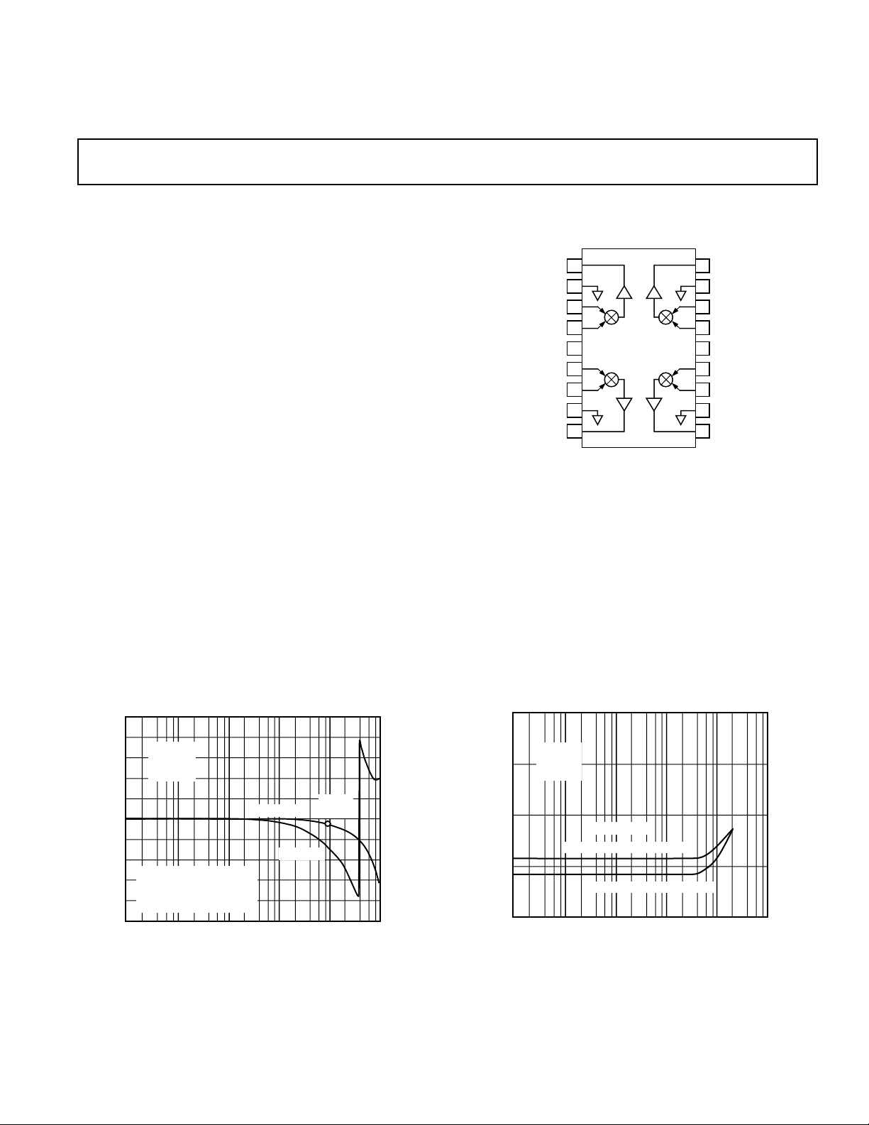
Four-Channel, Four-Quadrant
a
FEATURES
Four Independent Channels
Voltage IN, Voltage OUT
No External Parts Required
8 MHz Bandwidth
Four-Quadrant Multiplication
Voltage Output; W = (X × Y)/2.5 V
0.2% Typical Linearity Error on X or Y Inputs
Excellent Temperature Stability: 0.005%
±2.5 V Analog Input Range
Operates from ±5 V Supplies
Low Power Dissipation: 150 mW typ
Spice Model Available
APPLICATIONS
Geometry Correction in High-Resolution CRT Displays
Waveform Modulation & Generation
Voltage Controlled Amplifiers
Automatic Gain Control
Modulation and Demodulation
GENERAL DESCRIPTION
The MLT04 is a complete, four-channel, voltage output analog
multiplier packaged in an 18-pin DIP or SOIC-18. These complete
multipliers are ideal for general purpose applications such as voltage
controlled amplifiers, variable active filters, “zipper” noise free
audio level adjustment, and automatic gain control. Other applications include cost-effective multiple-channel power calculations
(I × V), polynomial correction generation, and low frequency
modulation. The MLT04 multiplier is ideally suited for generating
complex, high-order waveforms especially suitable for geometry
correction in high-resolution CRT display systems.
Analog Multiplier
MLT04
FUNCTIONAL BLOCK DIAGRAM
18-Lead Epoxy DIP (P Suffix)
18-Lead Wide Body SOIC (S Suffix)
Fabricated in a complementary bipolar process, the MLT04
includes four 4-quadrant multiplying cells which have been lasertrimmed for accuracy. A precision internal bandgap reference
normalizes signal computation to a 0.4 scale factor. Drift over
temperature is under 0.005%/°C. Spot noise voltage of 0.3 µV/√Hz
results in a THD + Noise performance of 0.02% (LPF = 22 kHz)
for the lower distortion Y channel. The four 8 MHz channels
consume a total of 150 mW of quiescent power.
The MLT04 is available in 18-pin plastic DIP, and SOIC-18
surface mount packages. All parts are offered in the extended
industrial temperature range (–40°C to +85°C).
100
40
V
= +5V
CC
VEE = –5V
TA = +25°C
20
Ø (X OR Y)
8.9MHz
–3dB
0
Av GAIN – dB
–20
X & Y MEASUREMENTS
SUPERIMPOSED:
X = 100mV RMS, Y = 2.5V DC
–40
Y = 100mV RMS, X = 2.5V DC
REV. B
Information furnished by Analog Devices is believed to be accurate and
reliable. However, no responsibility is assumed by Analog Devices for its
use, nor for any infringements of patents or other rights of third parties
which may result from its use. No license is granted by implication or
otherwise under any patent or patent rights of Analog Devices.
1k 10k 100M10M1M100k
Figure 1. Gain & Phase vs. Frequency Response
Av (X OR Y)
FREQUENCY – Hz
90
0
Ø – Phase Degrees
–90
THD + NOISE – %
0.01
One Technology Way, P.O. Box 9106, Norwood. MA 02062-9106, U.S.A.
Tel: 617/329-4700 Fax: 617/326-8703
V
= +5V
CC
V
= –5V
10
0.1
EE
T
= +25°C
A
1
10 100 1M100k10k1k
LPF = 500kHz
THDX: X = 2.5VP, Y = +2.5V DC
THDY: Y = 2.5VP, X = +2.5V DC
FREQUENCY – Hz
Figure 2. THD + Noise vs. Frequency

MLT04–SPECIFICATIONS
(VCC = +5 V, VEE = –5 V, VIN = ±2.5 VP, RL = 2 kΩ, TA = +25°C unless otherwise noted.)
Parameter Symbol Conditions Min Typ Max Units
MULTIPLIER PERFORMANCE
Total Error2 XE
Total Error
Linearity Error2 XLE
Linearity Error
2
YE
2
YLE
Total Error Drift TCE
Total Error Drift TCE
Scale Factor
3
Output Offset Voltage Z
Output Offset Drift TCZ
Offset Voltage, X X
Offset Voltage, Y Y
1
X
Y
X
Y
–2.5 V < X < +2.5 V, Y = +2.5 V –5 ±2 5 % FS
–2.5 V < Y < +2.5 V, X = +2.5 V –5 ±2 5 % FS
–2.5 V < X < +2.5 V, Y = +2.5 V –1 ±0.2 +1 % FS
–2.5 V < Y < +2.5 V, X = +2.5 V –1 ±0.2 +1 % FS
X = –2.5 V, Y = 2.5 V, TA = –40°C to +85°C 0.005 %/°C
X
Y = –2.5 V, X = 2.5 V, TA = –40°C to +85°C 0.005 %/°C
Y
K X = ±2.5 V, Y = ±2.5 V, TA = –40°C to +85°C 0.38 0.40 0.42 1/V
OS
OS
OS
X = 0 V, Y = 0 V, TA= –40°C to +85°C –50 ±10 50 mV
X = 0 V, Y = 0 V, TA= –40°C to +85°C50µV/°C
OS
X = 0 V, Y = ±2.5 V, TA = –40°C to +85°C –50 ±10.5 50 mV
Y = 0 V, X = ±2.5 V, TA = –40°C to +85°C –50 ±10.5 50 mV
DYNAMIC PERFORMANCE
Small Signal Bandwidth BW V
Slew Rate SR V
Settling Time t
AC Feedthrough FT
Crosstalk @ 100 kHz CT
S
AC
AC
= 0.1 V rms 8 MHz
OUT
= ±2.5 V 30 53 V/µs
OUT
V
= ∆2.5 V to 1% Error Band 1 µs
OUT
X = 0 V, Y = 1 V rms @ f = 100 kHz –65 dB
X = Y = 1 V rms Applied to Adjacent Channel –90 dB
OUTPUTS
Audio Band Noise E
Wide Band Noise E
Spot Noise Voltage e
N
N
N
Total Harmonic Distortion THD
THD
Open Loop Output Resistance R
Voltage Swing V
Short Circuit Current I
OUT
PK
SC
f = 10 Hz to 50 kHz 76 µV rms
Noise BW = 1.9 MHz 380 µV rms
f = 1 kHz 0.3 µV/√Hz
f = 1 kHz, LPF = 22 kHz, Y = 2.5 V 0.1 %
X
f = 1 kHz, LPF = 22 kHz, X = 2.5 V 0.02 %
Y
40 Ω
VCC = +5 V, VEE = –5 V ±3.0 ±3.3 V
30 mA
P
INPUTS
Analog Input Range IVR GND = 0 V –2.5 +2.5 V
Bias Current I
Resistance R
Capacitance C
B
IN
IN
X = Y = 0 V 2.3 10 µA
1MΩ
3pF
SQUARE PERFORMANCE
Total Square Error E
SQ
X = Y = 1 5 % FS
POWER SUPPLIES
V
Positive Current I
Negative Current I
Power Dissipation P
CC
EE
DISS
= 5.25 V, V
CC
V
= 5.25 V, V
CC
Calculated = 5 V × I
Supply Sensitivity PSSR X = Y = 0 V, V
Supply Voltage Range V
NOTES
1
Specifications apply to all four multipliers.
2
Error is measured as a percent of the ±2.5 V full scale, i.e., 1% FS = 25 mV.
3
Scale Factor K is an internally set constant in the multiplier transfer equation W = K × X × Y.
Specifications subject to change without notice.
RANGE
For VCC & V
= –5.25 V 15 20 mA
EE
= –5.25 V 15 20 mA
EE
= ∆5% or V
CC
EE
+ 5 V × I
CC
EE
= ∆5% 10 mV/V
EE
150 200 mW
±4.75 ±5.25 V
ABSOLUTE MAXIMUM RATINGS*
Supply Voltages V
Inputs X
Outputs W
, Y
I
I
, VEE to GND ±7 V
CC
I
VCC, V
VCC, V
EE
EE
Operating Temperature Range –40°C to +85°C
Maximum Junction Temperature (T
max) +150°C
J
Storage Temperature –65°C to +150°C
Lead Temperature (Soldering, 10 sec) +300°C
Package Power Dissipation (T
Thermal Resistance θ
JA
max–TA)/θ
J
JA
PDIP-18 (N-18) 74°C/W
SOIC-18 (SOL-18) 89°C/W
*Stresses above those listed under “Absolute Maximum Ratings” may cause perma-
nent damage to the device. This is a stress rating only and functional operation of
the device at these or any other conditions above those indicated in the operational
section of this specification are not implied.
–2–
ORDERING INFORMATION*
Temperature Package Package
Model Range Description Option
MLT04GP –40°C to +85°C 18-Pin P-DIP N-18
MLT04GS –40°C to +85°C 18-Lead SOIC SOL-18
MLT04GS-REEL –40°C to +85°C 18-Lead SOIC SOL-18
MLT04GBC +25°C Die
*For die specifications contact your local Analog sales office. The MLT04
contains 211 transistors.
REV. B
MLT04
50kΩ
–V
S
50kΩ
+V
S
±100mV
FOR X
OS
, YOS TRIM
CONNECT TO SUM
NODE OF AN EXT OP AMP
I
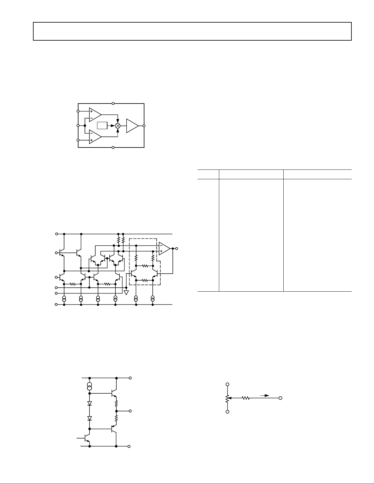
FUNCTIONAL DESCRIPTION
The MLT04 is a low cost quad, 4-quadrant analog multiplier with
single-ended voltage inputs and voltage outputs. The functional
block diagram for each of the multipliers is illustrated in Figure 3.
Due to packaging constraints, access to internal nodes for externally
adjusting scale factor, output offset voltage, or additional summing
signals is not provided.
+V
S
X1, X2, X3, X4
G1, G2, G3, G4
Y1, Y2, Y3, Y4
0.4
MLT04
W1, W2, W3, W4
–V
S
Figure 3. Functional Block Diagram of Each MLT04
Multiplier
Each of the MLT04’s analog multipliers is based on a Gilbert cell
multiplier configuration, a 1.23 V bandgap reference, and a unityconnected output amplifier. Multiplier scale factor is determined
through a differential pair/trimmable resistor network external to
the core. An equivalent circuit for each of the multipliers is shown
in Figure 4.
V
CC
W
SCALE
FACTOR
OUT
INTERNAL
BIAS
X
GND
Y
V
IN
IN
EE
22k
22k
200µA 200µA
200µA 200µA 200µA 200µA
22k
Figure 4. Equivalent Circuit for the MLT04
Details of each multiplier’s output-stage amplifier are shown in
Figure 5. The output stages idles at 200 µA, and the resistors in
series with the emitters of the output stage are 25 Ω. The output
stage can drive load capacitances up to 500 pF without oscillation.
For loads greater than 500 pF, the outputs of the MLT04 should
be isolated from the load capacitance with a 100 Ω resistor.
V
CC
ANALOG MULTIPLIER ERROR SOURCES
Multiplier errors consist primarily of input and output offsets, scale
factor errors, and nonlinearity in the multiplying core. An expression for the output of a real analog multiplier is given by:
= (K +∆K){(VX+ XOS)(VY+ YOS) + ZOS+ f(X , Y )}
V
O
where: K = Multiplier Scale Factor
∆K = Scale Factor Error
V
X
V
Y
Z
OS
ƒ(X, Y) = Nonlinearity
= X-Input Signal
X
= X-Input Offset Voltage
OS
= Y-Input Signal
Y
= Y-Input Offset Voltage
OS
= Multiplier Output Offset Voltage
Executing the algebra to simplify the above expression yields
expressions for all the errors in an analog multiplier:
Term Description Dependence on Input
KV
True Product Goes to Zero As Either or
XVY
Both Inputs Go to Zero
∆KVYVYScale-Factor Error Goes to Zero at VX, VY = 0
V
XYOS
Linear “X” Feedthrough Proportional to V
X
Due to Y-Input Offset
V
YXOS
Linear “Y” Feedthrough Proportional to V
Y
Due to X-Input Offset
X
OSYOS
Z
OS
Output Offset Due to X-, Independent of VX, V
Y-Input Offsets
Output Offset Independent of VX, V
Y
Y
ƒ(X, Y) Nonlinearity Depends on Both VX, VY.
Contains Terms Dependent
, VY, Their Powers
on V
X
and Cross Products
As shown in the table, the primary static errors in an analog
multiplier are input offset voltages, output offset voltage, scale
factor, and nonlinearity. Of the four sources of error, only two are
externally trimmable in the MLT04: the X- and Y-input offset
voltages. Output offset voltage in the MLT04 is factory-trimmed to
±50 mV, and the scale factor is internally adjusted to ±2.5% of full
scale. Input offset voltage errors can be eliminated by using the
optional trim circuit of Figure 6. This scheme then reduces the net
error to output offset, scale-factor (gain) error, and an irreducible
nonlinearity component in the multiplying core.
25Ω
W
OUT
25Ω
Figure 6. Optional Offset Voltage Trim Configuration
Figure 5. Equivalent Circuit for MLT04 Output Stages
REV. B
V
EE
–3–
MLT04
Feedthrough
In the ideal case, the output of the multiplier should be zero if
either input is zero. In reality, some portion of the nonzero input
will “feedthrough” the multiplier and appear at the output. This is
caused by the product of the nonzero input and the offset voltage of
the “zero” input. Introducing an offset equal to and opposite of the
“zero” input offset voltage will null the linear component of the
feedthrough. Residual feedthrough at the output of the multiplier
is then irreducible core nonlinearity.
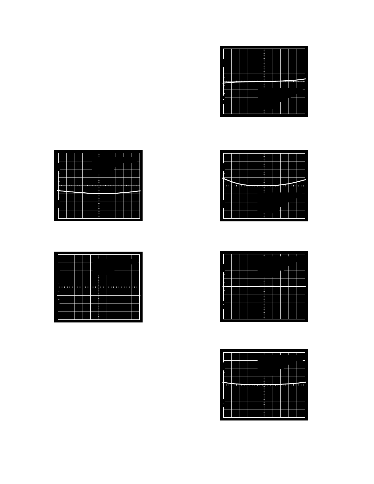
Typical X- and Y-input feedthrough curves for the MLT04 are
shown in Figures 7 and 8, respectively. These curves illustrate
MLT04 feedthrough after “zero” input offset voltage trim.
Residual X-input feedthrough measures 0.08% of full scale,
whereas residual Y-input feedthrough is almost immeasurable.
100
90
X-INPUT: ±2.5V @ 10Hz
10
VERTICAL – 5mV/DIV
0%
Y-INPUT: +2.5V
NULLED
Y
OS
T
= +25°C
A
HORIZONTAL – 0.5V/DIV
Figure 9. X-Input Nonlinearity @ Y = +2.5 V
100
90
10
VERTICAL – 5mV/DIV
0%
X-INPUT: ±2.5V @ 10Hz
NULLED
Y
OS
TA = +25°C
HORIZONTAL – 0.5V/DIV
Figure 7. X-Input Feedthrough with YOS Nulled
100
90
10
VERTICAL – 5mV/DIV
0%
Y-INPUT: ±2.5V @ 10Hz
NULLED
X
OS
TA = +25°C
HORIZONTAL – 0.5V/DIV
100
90
X-INPUT: ±2.5V @ 10Hz
10
VERTICAL – 5mV/DIV
0%
Y-INPUT: –2.5V
NULLED
Y
OS
T
= +25°C
A
HORIZONTAL – 0.5V/DIV
Figure 10. X-Input Nonlinearity @ Y = –2.5 V
Y-INPUT: ±2.5V @ 10Hz
100
90
10
VERTICAL – 5mV/DIV
0%
X-INPUT: +2.5V
NULLED
X
OS
TA = +25°C
HORIZONTAL – 0.5V/DIV
Figure 8. Y-Input Feedthrough with X
Nulled
OS
Nonlinearity
Multiplier core nonlinearity is the irreducible component of error.
It is the difference between actual performance and “best-straightline” theoretical output, for all pairs of input values. It is expressed
as a percentage of full scale with all other dc errors nulled. Typical
X- and Y-input nonlinearities for the MLT04 are shown in Figures
9 through 12. Worst-case X-input nonlinearity measured less than
0.2%, and Y-input nonlinearity measured better than 0.06%. For
modulator/demodulator or mixer applications it is, therefore,
recommended that the carrier be connected to the X-input while
the signal is applied to the Y-input.
–4–
Figure 11. Y-Input Nonlinearity @ X = +2.5 V
Y-INPUT: ±2.5V @ 10Hz
100
90
10
VERTICAL – 5mV/DIV
0%
X-INPUT: –2.5V
NULLED
X
OS
T
= +25°C
A
HORIZONTAL – 0.5V/DIV
Figure 12. Y-Input Nonlinearity @ X = –2.5 V
REV. B

T ypical Performance Characteristics – MLT04
FREQUENCY – Hz
1k 10k 100M10M1M100k
8
–2
–12
0
2
4
6
–10
–8
–6
–4
AV GAIN – dB
CL= 320pF
CL= 560pF
CL= 220pF
NO CL
CL= 100pF
VS = ±5V
RL = 2kΩ
TA = +25°C
10k 100k 10M1M
–12
12
0
–6
6
9
3
–3
–9
180
0
–90
90
135
45
–45
–135
–180
TA = +25°C
V
S
= ±5V
V
X
= +2.5V
V
Y
= 100mV
GAIN
PHASE
PHASE = 68.1
°
@ 8.064 MHz
FREQUENCY – Hz
GAIN –dB
PHASE – Degrees
NBW = 10Hz –50kHz
= +25°C
100
90
10
0%
OUTPUT NOISE VOLTAGE – 100µV/DIV
T
A
TIME = 10ms/DIV
Figure 13. Broadband Noise
NBW = 1.9MHz
= +25°C
100
90
T
A
12
9
6
3
0
GAIN –dB
–3
–6
–9
–12
10k 100k 10M1M
FREQUENCY – Hz
TA = +25°C
V
= ±5V
S
= 100mV
V
X
VY = +2.5V
GAIN
PHASE
PHASE = 68.3
@ 7.142 MHz
180
135
90
45
0
–45
–90
°
–135
–180
Figure 16. X-Input Gain and Phase vs. Frequency
PHASE – Degrees
REV. B
10
0%
OUTPUT NOISE VOLTAGE – 625µV/DIV
TIME = 10ms/DIV
Figure 14. Broadband Noise
10000
V
TA = +25°C
Hz
1000
100
NOISE DENSITY – nV/
0
10 100 1M100k10k1k
FREQUENCY – Hz
Figure 15. Noise Density vs. Frequency
S
= ±5V
Figure 17. Y-Input Gain and Phase vs. Frequency
Figure 18. Amplitude Response vs. Capacitive Load
–5–

MLT04 – Typical Performance Characteristics
VERTICAL – 50mV/DIV
TIME – 100ns/DIV
ΩX-INPUT = +2.5V
R
L
= 10kΩ
T
A
= +25°C
90
100
10
0%
TIME = 100ns/DIV
VERTICAL – 1V/DIV
ΩX-INPUT: +2.5V
R
L
= 10kΩ
T
A
= +25°C
90
100
10
0%
0
VS = ±5V
= +25°C
T
A
–20
–40
–60
FEEDTHROUGH – dB
–80
–100
10k 3M1M100k1k
FREQUENCY – Hz
VX = 0V
V
= 1V
Y
Figure 19. Feedthrough vs. Frequency
0
–20
–40
–60
CROSSTALK – dB
–80
–100
pk
VY = 0V
V
= 1V
X
pk
TA = 25°C
VS = ±5V
VX = ±2.5V
VY = +2.5VDC
pk
Figure 22. Y-Input Small-Signal Transient Response,
C
= 30 pF
L
ΩX-INPUT = +2.5V
R
100
90
10
VERTICAL – 50mV/DIV
0%
TIME – 100ns/DIV
T
= 10kΩ
L
= +25°C
A
Figure 23. Y-Input Small-Signal Transient Response,
= 100 pF
C
L
–120
10k 10M1M100k1k
FREQUENCY – Hz
Figure 20. Crosstalk vs. Frequency
2.0
1.5
1.0
0.5
0
–0.5
–1.0
AV GAIN – dB
–1.5
–2.0
–2.5
–3.0
1k 10k 100M10M1M100k
Figure 21. Gain Flatness vs. Frequency
Y = 100mV RMS
X = 2.5VDC
X = 100mV RMS
Y = 2.5VDC
FREQUENCY – Hz
ΩVS = ±5V
R
= 2kΩ
L
T
= +25°C
A
Figure 24. Y-Input Large-Signal Transient Response, C
= 30 pF
L
100
90
VERTICAL – 1V/DIV
10
0%
ΩX-INPUT: +2.5V
R
= 10kΩ
L
= +25°C
T
A
TIME = 100ns/DIV
–6–
Figure 25. Y-Input Large-Signal Transient Response,
CL = 100 pF
REV. B

1
–75 125–50
9
5
8
6
7
75 1005025
0
–25
80
60
75
65
70
V
S
= ±5V
V
X
= +2.5V
V
Y
= 100mV
PHASE @ –3dB BW – Degrees
–3dB-BANDWIDTH – MHz
TEMPERATURE – °C
–3dB BW
PHASE @ –3dB BW
4.5
4.0
0
10 100 10k1k
1.5
1.0
0.5
2.0
2.5
3.0
3.5
ΩLOAD RESISTANCE – Ω
OUTPUT SWING – Volts
VS = ±5V
T
A
= +25°C
POSITIVE SWING
NEGATIVE SWING
X-INPUT
Y = +2.5VDC
0.1
ΩVS = ±5V
R
= 2kΩ
THD + NOISE – %
0.01
0.001
L
T
= +25°C
A
f
= 1kHz
O
FLP F = 22kHz
0.1 1 10
INPUT SIGNAL LEVEL – Vol ts
Y-I NP UT
X = +2.5VDC
P-P
MLT04
Figure 26. THD + Noise vs. Input Signal Level
0.3
0.2
0.1
0
–0.1
LINEARTY ERROR – %
–0.2
–0.3
≤VX = +2.5V, –2.5V ≤ VY ≤ +2.5V
V
= +2.5V, –2.5V ≤ VX ≤ +2.5V
Y
0
TEMPERATURE – °C
Vs = ±5V
75–25
Figure 27. Linearity Error vs. Temperature
9
8
VS = ±5V
V
= 100mV
X
V
= +2.5V
Y
Figure 29. Y-Input Gain Bandwidth vs. Temperature
8
7
6
5
4
3
2
ΩTA = +25°C
= 2kΩ
R
MAXIMUM OUTPUT SWING – Volts p-p
125–50–75 1005025
L
V
S
= ±5V
10k 10M1M100k1k
FREQUENCY – Hz
1
0
1%
DISTORTION
Figure 30. Maximum Output Swing vs. Frequency
80
75
7
REV. B
–3dB-BANDWIDTH – MHz
6
5
–75 125–50
Figure 28. X-Input Gain Bandwidth vs. Temperature
–3dB BW
PHASE @ –3dB BW
0
–25
TEMPERATURE –
75 1005025
°
C
70
65
PHASE @ –3dB BW – Degrees
60
Figure 31. Maximum Output Swing vs. Resistive Load
–7–

MLT04
125–50–75 1007550250–25
TEMPERATURE –
°
C
0.407
0.402
0.405
0.403
0.404
0.406
SCALE FACTOR – 1/V
VS = ±5V
NO LOAD
300
SS = 1000 MULTIPLIERS
250
200
150
UNITS
100
50
0
XOS @ Y = ±2.5V
OFFSET VOLTAGE – mV
YOS @ X = ±2.5V
Figure 32. Offset Voltage Distribution
6
4
XOS, Y = ±2.5V
2
– mV
0
OS
V
–2
–4
–6
YOS, X = ±2.5V
TEMPERATURE –
°
C
TA = +25°C
V
= ±5V
S
X = ±2.5V
VS = ±5V
12.5–10–12.5 1052.50 7.5–2.5–5–7.5
Figure 35. Scale Factor vs. Temperature
400
SS = 1000
350
MULTIPLIERS
300
250
200
UNITS
150
100
50
125–50–75 1005025075–25
0
OUTPUT OFFSET VOLTAGE – mV
TA = +25°C
= ±5V
V
S
= VY = 0V
V
X
15–12–15 129630–3–6–9
UNITS
Figure 33. Offset Voltage vs. Temperature
400
SS = 1000 MULTIPLIERS
350
300
250
200
150
100
50
0
SCALE FACTOR – 1/V
T
A
V
S
= +25°C
= ±5V
Figure 34. Scale Factor Distribution
Figure 36. Output Offset Voltage (ZOS) Distribution
10
Vs = ±5V
5
0
–5
OUTPUT OFFSET VOLTAGE – mV
–10
0.4150.39750.395 0.41250.4100.40750.4050.40250.400
–75 125–50 75 10050250–25
TEMPERATURE –
°
C
Figure 37. Output Offset Voltage (ZOS) vs. Temperature
–8– REV.B

MLT04
17
16
15
SUPPLY CURRENT – mA
14
13
–75 125–50 75 10050250–25
TEMPERATURE –
VS = ±5V
NO LOAD
V
= VY = 0
X
°
C
Figure 38. Supply Current vs. Temperature
100
TA = +25°C
= ±5V
V
80
60
–PSRR
40
20
POWER SUPPLY REJECTION – dB
0
1k 1M100k10k100
FREQUENCY – Hz
+PSRR
S
15
12
9
6
3
0
–3
–6
–9
OUTPUT VOLTAGE OFFSET – mV
–12
–15
2000 1000800600400
HOURS OF OPERATION AT +125
σX +3σ
X
σX –3σ
°
C
Figure 41. Output Voltage Offset (ZOS) Distribution
Accelerated by Burn-in
0.424
0.420
0.416
0.412
0.408
0.404
0.400
0.396
SCALE FACTOR – 1/V
0.392
0.388
0.384
2000 1000800600400
HOURS OF OPERATION AT +125
°
C
σX +3σ
X
σX –3σ
Figure 39. Power Supply Rejection vs. Frequency
1.25
1.25
1.0
1.0
0.75
0.50
0.25
0
0
–0.25
–0.50
LINEARITY ERROR – %
–0.75
–1.0
–1.25
2000 1000800600400
HOURS OF OPERATION AT +125
σX +3σ
X
σX –3σ
°
C
Figure 40. Linearity Error (LE) Distribution Accelerated
by Burn-in
Figure 42. Scale Factor (K) Distribution Accelerated by Burn-in
–9–REV. B

MLT04
APPLICATIONS
The MLT04 is well suited for such applications as modulation/
demodulation, automatic gain control, power measurement, analog
computation, voltage-controlled amplifiers, frequency doublers,
and geometry correction in CRT displays.
Multiplier Connections
Figure 43 llustrates the basic connections for multiplication. Each
of the four independent multipliers has single-ended voltage inputs
(X, Y) and a low impedance voltage output (W). Also, each
multiplier has its own dedicated ground connection (GND) which
is connected to the circuit’s analog common. For best performance, circuit layout should be compact with short component
leads and well-bypassed supply voltage feeds. In applications where
fewer than four multipliers are used, all unused analog inputs must
be returned to the analog common.
+5V
0.1µF
W1
W2
1
W1
GND1
2
3
X1
Y1
Y2
X2
X1
Y1
4
V
5
CC
Y2
6
X2
7
GND2
8
9
W2
MLT04
123456789181716151413121110
GND4
V
GND3
W4
X4
Y3
X3
W3
18
17
16
15
Y4
14
EE
13
12
11
10
W4
Y4
X4
Y3
X3
W3
–5V
0.1µF
The equation shows a dc term at the output which will vary
strongly with the amplitude of the input, V
. The output dc offset
IN
can be eliminated by capacitively coupling the MLT04’s output
with a high-pass filter. For optimal spectral performance, the
filter’s cutoff frequency should be chosen to eliminate the input
fundamental frequency.
A source of error in this configuration is the offset voltages of the X
and Y inputs. The input offset voltages produce cross products
with the input signal to distort the output waveform. To circumvent this problem, Figure 45 illustrates the use of inverting
amplifiers configured with an OP285 to provide a means by which
the X- and Y-input offsets can be trimmed.
ΩP1
50kΩ
–5V
ΩR5
500kΩ
R1
10k
V
IN
R3
10k
ΩR6
500kΩ
–5V
50kΩ
+5V
X
TRIM
OS
R2
10k
2
A1
3
+
A1, A2 = 1/2 OP285
+
5
A2
6
R4
10k
YOS TRIM
+5V
ΩP2
1/4 MLT04
3
1
7
+
C1
100pF
2
0.4
+
4
W1
1
ΩR
L
10kΩ
V
O
W
1–4
= 0.4 (X
1–4
• Y
1–4
)
Figure 43. Basic Multiplier Connections
Squaring and Frequency Doubling
As shown in Figure 44, squaring of an input signal, V
by connecting the X-and Y-inputs in parallel to produce an output
2
of V
/2.5 V. The input may have either polarity, but the output
IN
, is achieved
IN
will be positive.
+5V
0.1µF
X
V
IN
GND
+
Y
+
0.4
1/4 MLT04
–5V
0.1µF
W
W = 0.4 V
2
IN
Figure 44. Connections for Squaring
When the input is a sine wave given by VIN sin ωt, the squaring
circuit behaves as a frequency doubler because of the trigonometric
identity:
Figure 45. Frequency Doubler with Input Offset Voltage
Trims
Feedback Divider Connections
The most commonly used analog divider circuit is the “inverted
multiplier” configuration. As illustrated in Figure 46, an “inverted
multiplier” analog divider can be configured with a multiplier
operating in the feedback loop of an operational amplifier. The
general form of the transfer function for this circuit configuration is
given by:
V
O
=−2.5V ×
R2
R1
IN
×
V
X
V
Here, the multiplier operates as a voltage-controlled potentiometer
that adjusts the loop gain of the op amp relative to a control signal,
VX. As the control signal to the multiplier decreases, the output of
the multiplier decreases as well. This has the effect of reducing
negative feedback which, in turn, decreases the amplifier’s loop
gain. The result is higher closed-loop gain and reduced circuit
bandwidth. As V
is increased, the output of the multiplier
X
increases which generates more negative feedback — closed-loop
gain drops and circuit bandwidth increases. An example of an
“inverted multiplier” analog divider frequency response is shown in
Figure 47.
2
2
(V
sinωt)
IN
2.5V
=
V
2.5V
1
IN
(1−cos 2ωt)
2
–10– REV. B

V
O
V
IN
=−
R2
R1
1
s
R2+R1
R1
2.5RC
V
X
+1
MLT04
V
O
V
IN
R1
10k
R2
10k
1/4 MLT04
0.4
3
2
4
1
Y1
X1
W1
6
OP113
D1
1N4148
VO = –2.5V • V
IN
2
3
+
X1
3
2
4
IN
X
GND1
Y1
+
V
V
O
R2
10k
W1
1/4 MLT04
1
+
0.4
+
R1
10k
V
IN
2
OP113
3
+
VO = –2.5V •
6
V
V
Figure 46. “Inverted-Multiplier” Configuration for
Analog Division
90
80
70
60
50
40
GAIN – dB
30
20
10
0
VX = 0.025V
V
VX = 2.5V
= 0.25V
X
A
VOL
OP113
X
Voltage-Controlled Low-Pass Filter
The circuit in Figure 49 illustrates how to construct a voltagecontrolled low-pass filter with an analog multiplier. The advantage
with this approach over conventional active-filter configurations is
that the overall characteristic cut-off frequency, ω
proportional to a multiplying input voltage. This permits the
, will be directly
O
construction of filters in which the capacitors are adjustable
(directly or inversely) by a control voltage. Hence, the frequency
scale of a filter can be manipulated by means of a single voltage
without affecting any other parameters. The general form of the
circuit’s transfer function is given by:
100 1k 10M1M100k10k
Figure 47. Signal-Dependent Feedback Makes Variables
Out of Amplifier Bandwidth and Stability
Although this technique works well with almost any operational
FREQUENCY – Hz
In this circuit, the ratio of R2 to R1 sets the passband gain, and the
=
, is given by:
LP
R1
R1+ R2
V
X
2.5RC
break frequency of the filter, ω
ω
LP
amplifier, there is one caveat: for best circuit stability, the unitygain crossover frequency of the operational amplifier should be
equal to or less than the MLT04’s 8 MHz bandwidth.
Connection for Square Rooting
Another application of the “inverted multiplier” configuration is the
square-root function. As shown in Figure 48, both inputs of the
MLT04 are wired together and are used as the output of the
circuit. Because the circuit configuration exhibits the following
generalized transfer function:
R2
×V
R1
IN
For example, if R1 = R2 = 10 kΩ , R = 10 kΩ , and C = 80 pF,
–11–REV. B
the input signal voltage is limited to the range –2.5 V ≤ VIN < 0. To
prevent circuit latchup due to positive feedback or input signal
polarity reversal, a 1N4148-type junction diode is used in series
with the output of the multiplier.
Figure 48. Connections for Square Rooting
V
=−2.5 ×
O
X1
V
X
GND1
R1
10k
3
2
+
V
IN
1/4 MLT04
+
0.4
+
4
Y1
V
O
= –
V
IN
1 + S
V
fLP =; f
X
π10πRC
= MAX @ VX = 2.5V
LP
R
10k
W1
1
2
A1
3
+
R2
A1 = 1/2 OP285
10k
1
5RC
V
X
Figure 49. A Voltage-Controlled Low-Pass Filter
C
80pF
1
V
O

MLT04
PIN 1
0.280 (7.11)
0.240 (6.10)
18
1
9
10
0.210
(5.33)
MAX
0.160 (4.06)
0.115 (2.93)
0.022 (0.558)
0.014 (0.356)
0.100
(2.54)
BSC
0.070 (1.77)
0.045 (1.15)
SEATING
PLANE
0.130
(3.30)
MIN
0.925 (23.49)
0.845 (21.47)
0.015
(0.38)
MIN
0.325 (8.25)
0.300 (7.62)
0.015 (0.38)
0.008 (0.20)
15°
0°
PIN 1
0.2992 (7.60)
0.2914 (7.40)
0.4193 (10.65)
0.3937 (10.00)
1
18
10
9
0.4625 (11.75)
0.4469 (11.35)
0.0192 (0.49)
0.0138 (0.35)
0.0500 (1.27)
BSC
0.1043 (2.65)
0.0926 (2.35)
0.0118 (0.30)
0.0040 (0.10)
0.0125 (0.32)
0.0091 (0.23)
0.0500 (1.27)
0.0157 (0.40)
8
°
0
°
0.0291 (0.74)
0.0098 (0.25)
x 45
°
then the output of the circuit has a pole at frequencies from 1 kHz
to 100 kHz for V
ranging from 25 mV to 2.5 V. The performance
X
of this low-pass filter is illustrated in Figure 20.
30
20
10
0
GAIN – dB
0.25V
– 10
VX = 0.025V
2.5V
– 20
– 30
10 100 10M1M100k10k1k
FREQUENCY – Hz
Figure 50. Low-Pass Cutoff Frequency vs. Control
Voltage, V
X
With this approach, it is possible to construct parametric biquad
filters whose parameters (center frequency, passband gain, and Q)
can be adjusted with dc control voltages.
OUTLINE DIMENSIONS
Dimensions shown in inches and (mm).
18-Lead Epoxy DIP (P Suffix)
C1845–18–10/93
18-Lead Wide-Body SOL (S Suffix)
PRINTED IN U.S.A.
–12– REV. B
 Loading...