

Page 1

LTC6652
V
ACCURACY (%)
0.050
Precision Low Drift Low
Noise Buffered Reference
Features
n
Low Drift:
A-Grade 5ppm/°C Max
B-Grade 10ppm/°C Max (MSOP8)
B-Grade 8ppm/°C Max (LS8)
n
High Accuracy:
A Grade ±0.05% Max
B-Grade ±0.1% Max
n
Low Noise: 2.1ppm
n
100% Tested at – 40°C, 25°C and 125°C
n
Sinks and Sources Current: ±5mA
n
Low Power Shutdown: <2µA Maximum
n
Thermal Hysteresis (LS8): 45ppm (–40°C to 125°C)
n
Long-Term Drift (LS8): 20ppm/√kHr
n
Low Dropout: 300mV
n
Available Output Voltage Options: 1.25V, 2.048V, 2.5V,
(0.1Hz to 10Hz)
P-P
3V, 3.3V, 4.096V, 5V
n
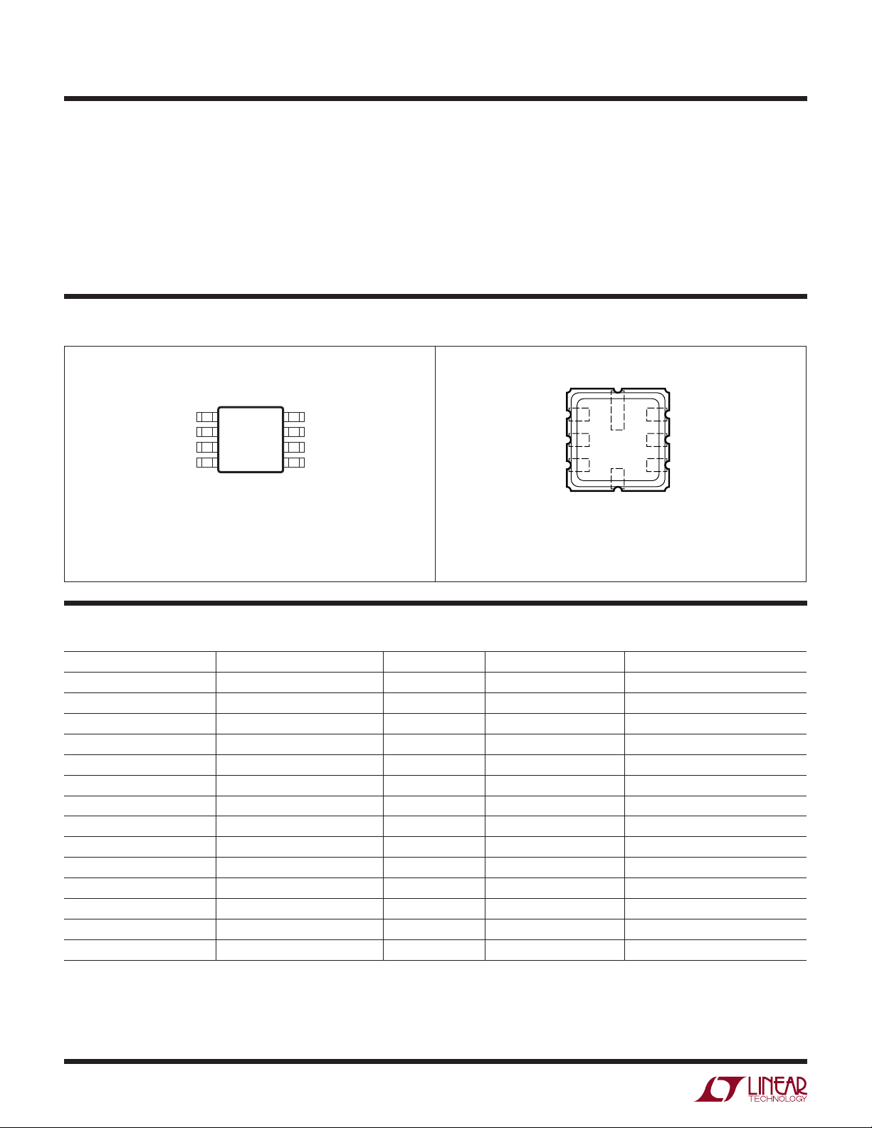
8-Lead MSOP and 5mm × 5mm Surface Mount
Hermetic Packages
applications
n
Automotive Control and Monitoring
n
High Temperature Industrial
n
High Resolution Data Acquisition Systems
n
Instrumentation and Process Control
n
Precision Regulators
n
Medical Equipment
Description
The LTC®6652 family of precision, low drift, low noise
references is fully specified over the temperature range
of –40°C to 125°C. High order curvature compensation
allows these references to achieve a low drift of less than
5ppm/°C with a predictable temperature characteristic and
an output voltage accuracy of ±0.05%. The performance
over temperature should appeal to automotive, high performance industrial and other high temperature applications.
The LTC6652 voltage references can be powered from
supply voltages up to 13.2V. They boast low noise, excellent load regulation, source and sink capability and
exceptional line rejection, making them a superior choice
for demanding precision applications. A shutdown mode
allows power consumption to be reduced when the reference is not needed. The optional output capacitor can be
left off when space constraints are critical.
The LTC6652 references are offered in an 8-lead MSOP
package and an 8-lead LS8 package. The LS8 is a 5mm
× 5mm surface mount hermetic package that provides
outstanding stability.
L, LT, LTC, LTM, Linear Technology and the Linear logo are registered trademarks of Linear
Technology Corporation. All other trademarks are the property of their respective owners.
typical application
Basic Connection
V
2.8V ≤ VIN ≤ 13.2V
0.1µF
(OPTIONAL)
C
IN
IN
SHDN
LTC6652-2.5
GND
Output Voltage Temperature Drift
0.025
V
C
OUT
1µF
(OPTIONAL)
6652 TA01a
OUT
2.5V
OUT
–0.025
–0.050
0
–20 0 20 40
–40
TEMPERATURE (°C)
60 80 100 125
6652 TA01b
6652fe
1
V
OUT
For more information www.linear.com/6652
Page 2
LTC6652
absolute MaxiMuM ratings
(Note 1)
Input Voltage
V
to GND ..........................................–0.3V to 13.2V
IN
SHDN to GND ............................–0.3V to (V
+ 0.3V)
IN
Output Voltage
V
...........................................–0.3V to (V
OUT
+ 0.3V)
IN
Output Short-Circuit Duration ...................... Indefinite
pin conFiguration
TOP VIEW
1
DNC
2
V
IN
3
SHDN
4
GND
MS8 PACKAGE
8-LEAD PLASTIC MSOP
= 150°C, θJA = 200°C/W
T
JMAX
DNC: DO NOT CONNECT
*CONNECT THE PINS TO DEVICE GND (PIN 4)
8
7
6
5
GND*
GND*
V
OUT
GND*
Operating Temperature Range ................ –40°C to 125°C
Storage Temperature Range (Note 2) ..... –65°C to 150°C
Lead Temperature Range (Soldering, 10 sec)
(Note 9)............................................................. 300°C
TOP VIEW
GND*
8
1
DNC
2
V
IN
SHDN
3
GND
8-PIN LEADLESS CHIP CARRIER (5mm × 5mm)
*CONNECT THE PINS TO DEVICE GND (PIN 4)
LS8 PACKAGE
= 150°C, θJA = 120°C/W
T
JMAX
DNC: DO NOT CONNECT
7
GND*
6
V
OUT
GND*
5
4
orDer inForMation
LEAD FREE FINISH TAPE AND REEL PART MARKING* PACKAGE DESCRIPTION SPECIFIED TEMPERATURE RANGE
LTC6652AHMS8-1.25#PBF LTC6652AHMS8-1.25#TRPBF LTCVH 8-Lead Plastic MSOP –40°C to 125°C
LTC6652BHMS8-1.25#PBF LTC6652BHMS8-1.25#TRPBF LTCVH 8-Lead Plastic MSOP –40°C to 125°C
LTC6652AHMS8-2.048#PBF LTC6652AHMS8-2.048#TRPBF LTCVJ 8-Lead Plastic MSOP –40°C to 125°C
LTC6652BHMS8-2.048#PBF LTC6652BHMS8-2.048#TRPBF LTCVJ 8-Lead Plastic MSOP –40°C to 125°C
LTC6652AHMS8-2.5#PBF LTC6652AHMS8-2.5#TRPBF LTCQV 8-Lead Plastic MSOP –40°C to 125°C
LTC6652BHMS8-2.5#PBF LTC6652BHMS8-2.5#TRPBF LTCQV 8-Lead Plastic MSOP –40°C to 125°C
LTC6652AHMS8-3#PBF LTC6652AHMS8-3#TRPBF LTCVK 8-Lead Plastic MSOP –40°C to 125°C
LTC6652BHMS8-3#PBF LTC6652BHMS8-3#TRPBF LTCVK 8-Lead Plastic MSOP –40°C to 125°C
LTC6652AHMS8-3.3#PBF LTC6652AHMS8-3.3#TRPBF LTCVM 8-Lead Plastic MSOP –40°C to 125°C
LTC6652BHMS8-3.3#PBF LTC6652BHMS8-3.3#TRPBF LTCVM 8-Lead Plastic MSOP –40°C to 125°C
LTC6652AHMS8-4.096#PBF LTC6652AHMS8-4.096#TRPBF LTCVN 8-Lead Plastic MSOP –40°C to 125°C
LTC6652BHMS8-4.096#PBF LTC6652BHMS8-4.096#TRPBF LTCVN 8-Lead Plastic MSOP –40°C to 125°C
LTC6652AHMS8-5#PBF LTC6652AHMS8-5#TRPBF LTCVP 8-Lead Plastic MSOP –40°C to 125°C
LTC6652BHMS8-5#PBF LTC6652BHMS8-5#TRPBF LTCVP 8-Lead Plastic MSOP –40°C to 125°C
2
6652fe
For more information www.linear.com/6652
Page 3

LTC6652
orDer inForMation
LEAD FREE FINISH PART MARKING* PACKAGE DESCRIPTION SPECIFIED TEMPERATURE RANGE
†
LTC6652AHLS8-2.5#PBF
LTC6652BHLS8-2.5#PBF
Consult LTC Marketing for parts specified with wider operating temperature ranges. *The temperature grade is identified by a label on the shipping container.
Consult LTC Marketing for information on non-standard lead based finish parts.
For more information on lead free part marking, go to: http://www.linear.com/leadfree/
For more information on tape and reel specifications, go to: http://www.linear.com/tapeandreel/
†
This product is only offered in trays. For more information go to: http://www.linear.com/packaging/
665225 8-Lead Ceramic LCC 5mm × 5mm –40°C to 125°C
†
665225 8-Lead Ceramic LCC 5mm × 5mm –40°C to 125°C
available options
OUTPUT VOLTAGE INITIAL ACCURACY TEMPERATURE COEFFICIENT PART NUMBER**
1.250 0.05%
0.1%
2.048 0.05%
0.1%
2.500 0.05%
0.1%
0.05%
0.1%
3.000 0.05%
0.1%
3.300 0.05%
0.1%
4.096 0.05%
0.1%
5.000 0.05%
0.1%
**See Order Information section for complete part number listing.
5ppm/°C
10ppm/°C
5ppm/°C
10ppm/°C
5ppm/°C
10ppm/°C
5ppm/°C
8ppm/°C
5ppm/°C
10ppm/°C
5ppm/°C
10ppm/°C
5ppm/°C
10ppm/°C
5ppm/°C
10ppm/°C
LTC6652AHMS8-1.25
LTC6652BHMS8-1.25
LTC6652AHMS8-2.048
LTC6652BHMS8-2.048
LTC6652AHMS8-2.5
LTC6652BHMS8-2.5
LTC6652AHLS8-2.5
LTC6652BHLS8-2.5
LTC6652AHMS8-3
LTC6652BHMS8-3
LTC6652AHMS8-3.3
LTC6652BHMS8-3.3
LTC6652AHMS8-4.096
LTC6652BHMS8-4.096
LTC6652AHMS8-5
LTC6652BHMS8-5
electrical characteristics
The l denotes the specifications which apply over the full operating
temperature range, otherwise specifications are at TA = 25°C, VIN = V
PARAMETER CONDITIONS MIN TYP MAX UNITS
Output Voltage LTC6652A
Output Voltage Temperature Coefficient
(Note 3)
Line Regulation V
Load Regulation (Note 4) I
LTC6652B
LTC6652A
LTC6652BMS8
LTC6652BLS8
+ 0.5V ≤ VIN ≤ 13.2V, SHDN = V
OUT
= 5mA, LTC6652-1.25, LTC6652-2.048,
SOURCE
LTC6652-2.5, LTC6652-3, LTC6652-3.3,
LTC6652-4.096, LTC6652-5
= 1mA, LTC6652-1.25, LTC6652-2.048
I
SINK
= 5mA, LTC6652-2.5, LTC6652-3,
I
SINK
LTC6652-3.3, LTC6652-4.096, LTC6652-5
For more information www.linear.com/6652
+ 0.5V, unless otherwise noted.
OUT
–0.05
–0.1
l
l
IN
l
l
l
l
2
0.05
0.1
4
4
2 50
20 75
80 250
50 150
5
10
8
80
200
600
450
ppm/°C
ppm/°C
ppm/°C
ppm/V
ppm/V
ppm/mA
ppm/mA
ppm/mA
ppm/mA
ppm/mA
ppm/mA
6652fe
3
%
%
Page 4

LTC6652
electrical characteristics
The l denotes the specifications which apply over the full operating
temperature range, otherwise specifications are at TA = 25°C, VIN = V
PARAMETER CONDITIONS MIN TYP MAX UNITS
Minimum Operating Voltage (Note 5) I
Output Short-Circuit Current Short V
Shutdown Pin (SHDN) Logic High Input Voltage
Supply Current No Load
Shutdown Current SHDN Tied to GND
Output Voltage Noise (Note 6) 0.1Hz ≤ f ≤ 10Hz
Turn-On Time 0.1% Settling, C
Long-Term Drift of Output Voltage (Note 7) LTC6652MS8
Hysteresis (Note 8) ∆T = –40°C to 125°C, LTC6652MS8
= 5mA, V
SOURCE
LTC6652-1.25, LTC6652-2.048
LTC6652-2.5, LTC6652-3, LTC6652-3.3,
LTC6652-4.096, LTC6652-5
to GND
OUT
OUT
to V
Short V
Logic High Input Current
Logic Low Input Voltage
Logic Low Input Current
LTC6652-1.25
LTC6652-2.048, LTC6652-2.5, LTC6652-3
LTC6652-3.3
LTC6652-4.096
LTC6652-5
10Hz ≤ f ≤ 1kHz
LTC6652LS8
∆T = –40°C to 85°C, LTC6652MS8
∆T = 0°C to 70°C, LTC6652MS8
∆T = –40°C to 125°C, LTC6652LS8
∆T = –40°C to 85°C, LTC6652LS8
∆T = 0°C to 70°C, LTC6652LS8
Error ≤ 0.1%
OUT
IN
= 0 100 µs
LOAD
+ 0.5V, unless otherwise noted.
OUT
l
l
l
l
l
l
l
l
2.7
+ 0.3V
V
OUT
2
16
16
0.1
0.1
350
0.1 2 µA
2.4
2.1
2.2
2.3
2.8
3
60
20
80
75
45
45
25
10
1
0.8
1
560
mA
mA
ppm
ppm
ppm
ppm
ppm
ppm
RMS
ppm/√kHr
ppm/√kHr
ppm
ppm
ppm
ppm
ppm
ppm
µA
µA
µA
µA
P-P
P-P
P-P
P-P
P-P
V
V
V
V
Note 1: Stresses beyond those listed under Absolute Maximum Ratings
may cause permanent damage to the device. Exposure to any Absolute
Maximum Rating condition for extended periods may affect device
reliability and lifetime.
Note 2: If the parts are stored outside of the specified temperature range,
the output may shift due to hysteresis.
Note 3: Temperature coefficient is measured by dividing the maximum
change in output voltage by the specified temperature range.
Note 4: Load regulation is measured on a pulse basis from no load to the
specified load current. Output changes due to die temperature change
must be taken into account separately.
Note 5: Excludes load regulation errors.
Note 6: Peak-to-peak noise is measured with a 3-pole highpass at 0.1Hz
and 4-pole lowpass filter at 10Hz. The unit is enclosed in a still-air
environment to eliminate thermocouple effects on the leads. The test
time is 10 seconds. RMS noise is measured on a spectrum analyzer in
a shielded environment where the intrinsic noise of the instrument is
removed to determine the actual noise of the device.
Note 7: Long-term stability typically has a logarithmic characteristic and
therefore, changes after 1000 hours tend to be much smaller than before that
time. Total drift in the second thousand hours is normally less than one third
that of the first thousand hours with a continuing trend toward reduced drift
with time. Long-term stability will also be affected by differential stresses
between the IC and the board material created during board assembly.
Note 8: Hysteresis in output voltage is created by package stress that differs
depending on whether the IC was previously at a higher or lower temperature.
Output voltage is always measured at 25°C, but the IC is cycled to the hot
or cold temperature limit before successive measurements. Hysteresis
is roughly proportional to the square of the temperature change. For
instruments that are stored at well controlled temperatures (within 20 or 30
degrees of operational temperature) it’s usually not a dominant error source.
Typical hysteresis is the worst-case of 25°C to cold to 25°C or 25°C to hot to
25°C, preconditioned by one thermal cycle.
Note 9: The stated temperature is typical for soldering of the leads during
manual rework. For detailed IR reflow recommendations, refer to the
Applications section.
6652fe
4
For more information www.linear.com/6652
Page 5
LTC6652
NOISE VOLTAGE (nV/√Hz)
OUTPUT NOISE (1µV/DIV)
OUTPUT VOLTAGE (V)
REFERENCE VOLTAGE (V)
1.2510
OUTPUT VOLTAGE CHANGE (ppm)
OUTPUT VOLTAGE CHANGE (ppm)
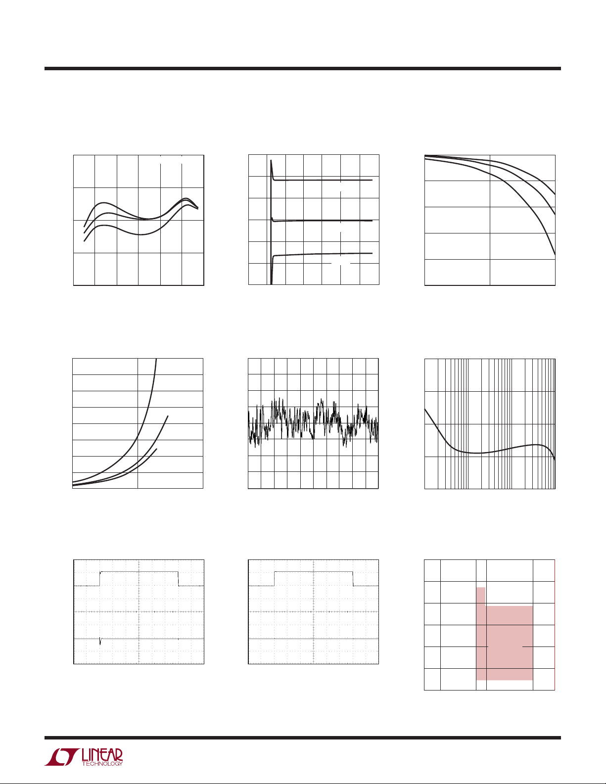
typical perForMance characteristics
Characteristic curves are similar for most
LTC6652s. Curves from the LTC6652-1.25, LTC6652-2.5 and the LTC6652-5 represent the extremes and typical of the voltage options.
Characteristic curves for other output voltages fall between these curves and can be estimated based on their output.
1.25V Output Voltage
Temperature Drift
1.2505
1.2500
1.2495
1.2490
–80
–40 0
40 160
TEMPERATURE (°C)
1.25V Load Regulation (Sinking)
400
350
300
250
200
150
100
50
0
0.1
OUTPUT CURRENT (mA)
–40°C
1 10
3 TYPICAL PARTS
80
120
6652 G17
125°C
25°C
6652 G20
1.25V Line Regulation
1.2506
1.2504
1.2502
1.2500
1.2498
1.2496
1.2494
0
2 4
6 10
INPUT VOLTAGE (V)
1.25V Low Frequency 0.1Hz to
10Hz Transient Noise
TIME (1 SECOND/DIV)
125°C
25°C
–40°C
8 12 14
6652 G18
6652 G21
1.25V Load Regulation (Sourcing)
0
–50
–100
–150
–200
–250
0.1
OUTPUT CURRENT (mA)
125°C
1
1.25V Output Voltage Noise
Spectrum
400
300
200
100
0
0.01
0.1 1 10
FREQUENCY (kHz)
–40°C
25°C
10
6652 G19
6652 G22
I
OUT
500mV/DIV
1.25 Sinking Current Without
Output Capacitor
1mA
0mA
V
OUT
C
= 0µF
OUT
500µs/DIV
6652 G23
1.25 Sinking Current with Output
Capacitor
1mA
I
OUT
0mA
V
OUT
500mV/DIV
C
= 1µF
OUT
For more information www.linear.com/6652
500µs/DIV
6652 G24
1.25V Stability with Output
Capacitance
10µF
1µF
0.1µF
10nF
1nF
OUTPUT CAPACITOR
100pF
NO CAP
–5 –1 0 5
LOAD CURRENT (mA)
REGION OF
MARGINAL
STABILITY
6652 G16
6652fe
5
Page 6

LTC6652
typical perForMance characteristics
Characteristic curves are similar for most
LTC6652s. Curves from the LTC6652-1.25, LTC6652-2.5 and the LTC6652-5 represent the extremes and typical of the voltage options.
Characteristic curves for other output voltages fall between these curves and can be estimated based on their output.
2.5V Output Voltage
Temperature Drift
2.5010
2.5005
2.5000
2.4995
REFERENCE VOLTAGE (V)
2.4990
2.4985
–50
–25 0
50
25 75 150
TEMPERATURE (°C)
2.5V Load Regulation (Sinking)
700
600
500
400
200
100
OUTPUT VOLTAGE CHANGE (ppm)
0
0.1
OUTPUT CURRENT (mA)
1 10
3 TYPICAL PARTS
100 125
125°C
25°C
–40°C
6652 G01
6652 G04
2.5V Line Regulation
2.5010
2.5005
2.5000
2.4995
2.4990
OUTPUT VOLTAGE (V)
2.4985
2.4980
0
2 4
2.5V Supply Current
vs Input Voltage
1000
900
800
700
600
500
400
300
SUPPLY CURRENT (µA)
200
100
0
0
2
8 12 14
6 10
INPUT VOLTAGE (V)
125°C
25°C
–40°C
8
6
4
INPUT VOLTAGE (V)
125°C
25°C
–40°C
10
12
6652 G02
6652 G05
14
2.5V Load Regulation (Sourcing)
0
–20
–40
–60
–80
–100
–120
–140
–160
OUTPUT VOLTAGE CHANGE (ppm)
–180
–200
0.1
OUTPUT CURRENT (mA)
1
2.5V Shutdown Current
vs Input Voltage
1.0
0.9
0.8
0.7
0.6
0.5
0.4
0.3
SUPPLY CURRENT (µA)
0.2
0.1
0
0
2
125°C
25°C
–40°C
8
6
4
INPUT VOLTAGE (V)
125°C
10
–40°C
25°C
12
10
6652 G03
14
6652 G06
6
2.5V Minimum V
Differential (Sourcing)
10
1
25°C
0.1
OUTPUT CURRENT (mA)
0.01
0.001
125°C, –40°C
0.01 0.1 1
INPUT-OUTPUT VOLTAGE (V)
IN-VOUT
6652 G09
For more information www.linear.com/6652
2.5V Minimum V
Differential (Sinking)
10
1
OUTPUT CURRENT (mA)
0.1
0.001
25°C
125°C
0.01 0.1 1
OUTPUT-INPUT VOLTAGE (V)
OUT-VIN
–40°C
6652 G10
6652fe
Page 7

LTC6652
typical perForMance characteristics
Characteristic curves are similar for most
LTC6652s. Curves from the LTC6652-1.25, LTC6652-2.5 and the LTC6652-5 represent the extremes and typical of the voltage options.
Characteristic curves for other output voltages fall between these curves and can be estimated based on their output.
2.5V Low Frequency 0.1Hz to
10Hz Transient Noise
OUTPUT NOISE (1µV/DIV)
TIME (1 SECOND/DIV)
Typical V
Distribution for
OUT
LTC6652-2.5
180
1004 UNITS
160
140
120
80
60
NUMBER OF UNITS
40
20
0
2.4985
LTC6652A LIMITS
2.4995 2.5015
OUTPUT VOLTAGE (V)
2.5005
6652 G11
6652 G15
2.5V Output Voltage Noise
Spectrum
600
500
400
300
200
NOISE VOLTAGE (nV/√Hz)
100
0
0.01
0.1 1 10
FREQUENCY (kHz)
Stability with Output Capacitance
(LTC6652-2.5, LTC6652-3,
LTC6652-3.3, LTC6652-4.096,
LTC6652-5)
10µF
1µF
0.1µF
10nF
1nF
OUTPUT CAPACITOR
100pF
NO CAP
–5 0 5
REGION OF
MARGINAL STABILITY
LOAD CURRENT (mA)
6652 G12
6652 G14
For more information www.linear.com/6652
6652fe
7
Page 8

LTC6652
NOISE VOLTAGE (nV/√Hz)
OUTPUT NOISE (5µV/DIV)
SUPPLY CURRENT (µA)
OUTPUT VOLTAGE (V)
5.002
REFERENCE VOLTAGE (V)
SUPPLY CURRENT (µA)
OUTPUT CURRENT (mA)
10
typical perForMance characteristics
Characteristic curves are similar for most
LTC6652s. Curves from the LTC6652-1.25, LTC6652-2.5 and the LTC6652-5 represent the extremes and typical of the voltage options.
Characteristic curves for other output voltages fall between these curves and can be estimated based on their output.
5V Output Voltage
Temperature Drift
5.005
5.003
5.000
4.998
4.995
–50 25 75 150
–25 0
TEMPERATURE (°C)
3 TYPICAL PARTS
50
100 125
5V Shutdown Current
vs Input Voltage
1.0
0.9
0.8
0.7
0.6
0.5
0.4
0.3
0.2
0.1
0
0
2
6
4
INPUT VOLTAGE (V)
125°C
–40°C
25°C
8
10
12
6652 G25
6652 G29
5V Line Regulation
5.001
25°C
5.000
125°C
4.999
4.998
0
2 4
5V Minimum VIN to V
6 10
INPUT VOLTAGE (V)
–40°C
8 12 14
6652 G26
OUT
Differential (Sourcing)
1
25°C
0.1
–40°C
125°C
0.01
14
0.001
0.01 0.1 1
INPUT-OUTPUT VOLTAGE (V)
6652 G30
5V Supply Current
vs Input Voltage
1000
900
800
700
600
500
400
300
200
100
0
0
4
2
INPUT VOLTAGE (V)
125°C
25°C
–40°C
8
6
5V Low Frequency 0.1Hz to 10Hz
Transient Noise
TIME (1 SECOND/DIV)
12
14
6652 G27
6652 G31
10
1000
800
600
400
200
8
5V Output Voltage Noise Spectrum
0
0.01
0.1 1 10
FREQUENCY (kHz)
6652 G32
5V Start-Up Response Without
Output Capacitor
V
IN
2V/DIV
V
OUT
2V/DIV
= 0µF
C
OUT
For more information www.linear.com/6652
100µs/DIV
6652 G33
5V Start-Up Response with Output
Capacitor
V
IN
2V/DIV
V
OUT
2V/DIV
= 1µF
C
OUT
100µs/DIV
6652 G34
6652fe
Page 9

LTC6652
typical perForMance characteristics
Characteristic curves are similar for most
LTC6652s. Curves from the LTC6652-1.25, LTC6652-2.5 and the LTC6652-5 represent the extremes and typical of the voltage options.
Characteristic curves for other output voltages fall between these curves and can be estimated based on their output.
Power Supply Rejection Ratio
vs Frequency
0
–10
–20
–30
–40
–50
–60
–70
–80
–90
POWER SUPPLY REJECTION RATIO (dB)
–100
0.01
0.1 1 10 100 1000
C
OUT
FREQUENCY (kHz)
= 0µF
C
OUT
C
OUT
= 10µF
= 1µF
6652 G07
Output Impedance vs Frequency
100
10
1
OUTPUT IMPEDANCE (Ω)
0.1
0.01 1 10 100
pin Functions
DNC (Pin 1): Do Not Connect.
(Pin 2): Power Supply. The minimum supply input is
V
IN
+ 300mV or 2.7V; whichever is higher. The maximum
V
OUT
supply is 13.2V. Bypassing V
GND will improve PSRR.
with a 0.1µF capacitor to
IN
C
OUT
C
0.1
FREQUENCY (kHz)
SHDN Input Voltage Thresholds
vs V
1.5
0.5
IN
V
TH(UP)
V
TH(DN)
0
2
4
8 12 14
6 10
VIN (V)
6652 G13
= 1µF
OUT
C
OUT
= 10µF
= 0µF
6652 G08
(V)
TRIP
V
2.5
2.0
1.0
GND (Pin 4): Device Ground.
(Pin 6): Output Voltage. An output capacitor is not
V
OUT
required. For some applications, a capacitor between 0.1µF
to 10µF can be beneficial. See the graphs in the Typical
Performance Characteristics section for further details.
SHDN (Pin 3): Shutdown Input. This active low input
powers down the device to <2µA. For normal operation
tie this pin to V
IN
.
GND (Pins 5,7,8): Internal Function. Ground these pins.
6652fe
For more information www.linear.com/6652
9
Page 10

LTC6652
block DiagraM
V
IN
2
SHDN
3 6
GND
4
BANDGAP
applications inForMation
Bypass and Load Capacitors
The LTC6652 voltage references do not require an input
capacitor, but a 0.1µF capacitor located close to the part
improves power supply rejection.
The LTC6652 voltage references are stable with or without
a capacitive load. For applications where an output capacitor is beneficial, a value of 0.1µF to 10µF is recommended
depending on load conditions. The Typical Performance
Characteristics section includes a plot illustrating a region
of marginal stability. Either no or low value capacitors for
any load current are acceptable. For loads that sink current
or light loads that source current, a 0.1µF to 10µF capacitor
has stable operation. For heavier loads that source current
a 0.5µF to 10µF capacitor range is recommended.
+
–
The transient response for a 0.5V step on V
6652 BD
V
OUT
with and
IN
without an output capacitor is shown in Figures 2 and 3,
respectively.
The LTC6652 references with an output of 2.5V and above
are guaranteed to source and sink 5mA. The 1.25V and
2.048V versions are guaranteed to source 5mA and sink
1mA. The test circuit for transient load step response is
shown in Figure 1. Figures 4 and 5 show a 5mA source
and sink load step response without a load capacitor,
respectively.
Start-Up
The start-up characteristic of the LTC6652 is shown in
Figures 8 and 9. Note that the turn-on time is affected by
the value of the output capacitor.
10
2, 3 6
V
IN
3V
C
IN
0.1µF
Figure 1. Transient Load Test Circuit
For more information www.linear.com/6652
LTC6652-2.5
4, 5, 7, 8
100Ω
C
OUT
1µF
V
6652 F01
GEN
0.5V
6652fe
Page 11

applications inForMation
LTC6652
3.5V
V
IN
3V
V
OUT
500mV/DIV
C
OUT
= 0µF
500µs/DIV
6652 F02
Figure 2. Transient Response Without Output Capacitor
3.5V
V
IN
3V
V
OUT
500mV/DIV
5mA
I
OUT
0mA
V
OUT
200mV/DIV
0mA
I
OUT
–5mA
V
OUT
200mV/DIV
C
OUT
= 0µF
250µs/DIV
Figure 5. LTC6652-2.5 Sinking
Current Without Output Capacitor
6652 F05
C
= 1µF
OUT
500µs/DIV
6652 F03
Figure 3. Transient Response with 1µF Output Capacitor
0mA
I
OUT
–5mA
V
OUT
200mV/DIV
C
OUT
= 0µF
250µs/DIV
6652 F04
Figure 4. LTC6652-2.5 Sourcing
Current Without Output Capacitor
5mA
I
OUT
0mA
V
OUT
50mV/DIV
C
= 1µF
OUT
250µs/DIV
6652 F06
Figure 6. LTC6652-2.5 Sourcing Current
with Output Capacitor
C
= 1µF
OUT
250µs/DIV
6652 F07
Figure 7. LTC6652-2.5 Sinking
Current with Output Capacitor
For more information www.linear.com/6652
6652fe
11
Page 12

LTC6652
applications inForMation
V
IN
2V/DIV
V
OUT
1V/DIV
C
= 0µF
OUT
100µs/DIV
6652 F08
Figure 8. Start-Up Response without Output Capacitor
V
IN
2V/DIV
V
OUT
1V/DIV
2.8V ≤ VIN ≤ 13.2V
Figure 10. Open-Drain Shutdown Circuit
SHDN
1V/DIV
V
OUT
1V/DIV
I
LOAD
TO µC
= 5mA
C1
1µF
R1
20k
SHDN
2N7002
1ms/DIV
V
IN
LTC6652-2.5
GND
V
6652 F10
OUT
6652 F11
C2
1µF
V
OUT
C
OUT
= 1µF
100µs/DIV
6652 F09
Figure 9. Start-Up Response with 1µF Output Capacitor
In Figure 8, ripple momentarily appears just after the
leading edge of powering on. This brief one time event is
caused by calibration circuitry during initialization. When
an output capacitor is used, the ripple is virtually undetectable as shown in Figure 9.
Shutdown Mode
Shutdown mode is enabled by tying SHDN low which
places the part in a low power state (i.e., <2µA). In shut-
down mode, the output pin takes the value 20k • (rated
output voltage). For example, an LTC6652-2.5 will have
Figure 11. Shutdown Response with 5mA Load
an output impedance of 20k • 2.5 = 50kΩ. For normal
operation, SHDN should be greater than or equal to 2.0V.
For use with a microcontroller, use a pull-up resistor to
and an open-drain output driver as shown in Figure
V
IN
10. The LTC6652’s response into and out of shutdown
mode is shown in Figure 11.
The trip thresholds on SHDN have some dependence on the
voltage applied to V
as shown in the Typical Performance
IN
Characteristics section. Be careful to avoid leaving SHDN
at a voltage between the thresholds as this will likely cause
an increase in supply current due to shoot-through current.
12
6652fe
For more information www.linear.com/6652
Page 13

applications inForMation
LTC6652
80
LTC6652-2.5 MS8 PACKAGE
3 TYPICAL PARTS
= 35°C
T
60
A
40
20
ppm
0
–20
–40
0
300 600 1200 1500
900
HOURS
Figure 12a. MS8 Long-Term Drift
35
25°C TO 125°C TO 25°C 25°C TO –40°C TO 25°C
30
25
20
15
NUMBER OF UNITS
10
5
0
–250 –150 –50
DISTRIBUTION (ppm)
6652 F12a
15050
6652 F13a
80
LTC6652-2.5 LS8 PACKAGE
4 TYPICAL PARTS
= 30°C
T
60
A
40
20
ppm
0
–20
–40
0
200 400 800 1000
600
HOURS
Figure 12b. LS8 Long-Term Drift
9
25°C TO 125°C TO 25°C
8
7
6
5
4
3
NUMBER OF UNITS
2
1
0
–110 –80 –50 –20 0 5020 80
DISTRIBUTION (ppm)
25°C TO –40°C TO 25°C
6652 F12b
110
6652 F13b
Figure 13a. MS8 Hysteresis Plot –40°C to 125°C Figure 13b. LS8 Hysteresis Plot –40°C to 125°C
Long-Term Drift
Long-term drift cannot be extrapolated from accelerated
high temperature testing. This erroneous technique gives
drift numbers that are wildly optimistic. The only way
long-term drift can be determined is to measure it over
the time interval of interest. The LTC6652 long-term drift
data was collected on more than 100 parts that were soldered into PC boards similar to a “real world” application.
The boards were then placed into a constant temperature
oven with T
= 35°C, their outputs were scanned regularly
A
and measured with an 8.5 digit DVM. Long-term drift is
shown below in Figure 12.
For more information www.linear.com/6652
Hysteresis
The hysteresis data shown in Figure 13 represents the
worst-case data collected on parts from –40°C to 125°C.
The output is capable of dissipating relatively high power,
i.e., for the LTC6652-2.5, P
= 10.7V • 5.5mA = 58.85mW.
D
The thermal resistance of the MS8 package is 200°C/W
and this dissipation causes a 11.8°C internal rise. This
could increase the junction temperature above 125°C and
may cause the output to shift due to thermal hysteresis.
6652fe
13
Page 14

LTC6652
300
applications inForMation
PC Board Layout
The mechanical stress of soldering a surface mount voltage reference to a PC board can cause the output voltage
to shift and temperature coefficient to change. These two
changes are not correlated. For example, the voltage may
shift, but the temperature coefficient may not.
To reduce the effects of stress-related shifts, mount the
reference near the short edge of the PC board or in a
corner. In addition, slots can be cut into the board on two
sides of the device.
The capacitors should be mounted close to the package.
The GND and V
traces should be as short as possible
OUT
to minimize I • R drops. Excessive trace resistance directly
impacts load regulation.
IR Reflow Shift
The different expansion and contraction rates of the materials that make up the lead-free LTC6652 package cause the
output voltage to shift after undergoing IR reflow. Lead-free
reflow profiles reach over 250°C, considerably more than
their leaded counterparts. The lead-free IR reflow profile
used to experimentally measure output voltage shift in the
LTC6652-2.5 is shown in Figure 14. Similar results can be
380s
TP = 260°C
225
TS = 190°C
T = 150°C
150
RAMP TO
150°C
75
0
0 2 4 6
Figure 14. Lead-Free Reflow Profile
T
S(MAX)
TL = 217°C
= 200°C
120s
MINUTES
t
30s
t
130s
40s
RAMP
DOWN
P
L
10
8
6652 F14
expected using a convection reflow oven. In our experiment,
the serialized parts were run through the reflow process
twice. The results indicate that the standard deviation of
the output voltage increases with a slight positive mean
shift of 0.003% as shown in Figure 15. While there can
be up to 0.016% of output voltage shift, the overall drift
of the LTC6652 after IR reflow does not vary significantly.
Power Dissipation
Power dissipation in the LTC6652 is dependent on V
IN
,
load current, and package. The LTC6652 package has
a thermal resistance, or θ
, of 200°C/W. A curve that
JA
illustrates allowed power dissipation vs temperature for
this package is shown in Figure 16.
The power dissipation of the LTC6652-2.5V as a function
of input voltage is shown in Figure 17. The top curve
shows power dissipation with a 5mA load and the bottom
curve shows power dissipation with no load.
When operated within its specified limits of V
= 13.2V
IN
and sourcing 5mA, the LTC6652-2.5 consumes just under
60mW at room temperature. At 125°C the quiescent current will be slightly higher and the power consumption
increases to just over 60mW. The power-derating curve
in Figure 16 shows the LTC6652-2.5 can safely dissipate
125mW at 125°C about half the maximum power consumption of the package.
Humidity Sensitivity
Plastic mould compounds absorb water. With changes
in relative humidity, plastic packaging materials change
the amount of pressure they apply to the die inside,
which can cause slight changes in the output of a voltage reference, usually on the order of 100ppm. The LS8
package is hermetic, so it is not affected by humidity, and
is therefore more stable in environments where humidity
may be a concern.
14
6652fe
For more information www.linear.com/6652
Page 15

applications inForMation
LTC6652
10
8
6
4
NUMBER OF UNITS
2
0
–0.014 –0.006
OUTPUT VOLTAGE SHIFT DUE TO IR REFLOW (%)
0.0180.0100.002
6652 F15a
Figure 15a. MS8 Output Voltage Shift Due to IR Reflow
0.7
0.6
0.5
0.4
0.3
DISSIPATION (W)
0.2
0.1
0
0
40
20
TEMPERATURE (°C)
60 140
80
100 120
6652 F16
7
1X
3X
6
5
4
3
NUMBER OF UNITS
2
1
0
–0.1 –0.02–0.06
OUTPUT VOLTAGE SHIFT DUE TO IR REFLOW (%)
0.060.020
0.1
6652 F15b
Figure 15b. LS8 Output Voltage Shift Due to IR Reflow
0.06
TA = 25°C
0.05
0.04
5mA LOAD
0.03
POWER (W)
0.02
0.01
0
2
4
NO LOAD
6
8 14
VIN (V)
10 12
6652 F17
Figure 16. Maximum Recommended Dissipation for LTC6652
For more information www.linear.com/6652
Figure 17. Typical Power Dissipation of the LTC6652
6652fe
15
Page 16

LTC6652
VCC ≥ 1.75V
typical applications
Extended Supply Range Reference Extended Supply Range Reference
4V TO 30V
R1
BZX84C18
V
LTC6652-2.5
IN
SHDN
C1
0.1µF
Negative Rail Circuit
C1
0.1µF
6
LTC6652-2.5
VEE ≤ –3V
GND
2, 3
4, 5, 7, 8
500Ω
V
OUT
6652 TA02
1µF
6652 TA06
V
OUT
–2.5V
V
OUT
C2
OPTIONAL
R1
330k
V+ ≥ (V
R2
4.7k
BZX84C18
+ 1.8V)
OUT
6V TO 160V
ON SEMI
MMBT5551
V
SHDN
IN
GND
V
OUT
6652 TA03
LTC6652-2.5
C1
0.1µF
Boosted Output Current
C1
1µF
R1
220Ω
V
IN
LTC6652-2.5
GND
SHDN
6652 TA04
V
OUT
C2
OPTIONAL
2N2905
V
C2
1µF
OUT
V
OUT
16
6652fe
For more information www.linear.com/6652
Page 17

package Description
Please refer to http://www.linear.com/designtools/packaging/ for the most recent package drawings.
MS8 Package
8-Lead Plastic MSOP
(Reference LTC DWG # 05-08-1660 Rev F)
LTC6652
0.889 ± 0.127
(.035 ± .005)
5.23
(.206)
MIN
0.42 ± 0.038
(.0165 ± .0015)
TYP
RECOMMENDED SOLDER PAD LAYOUT
NOTE:
1. DIMENSIONS IN MILLIMETER/(INCH)
2. DRAWING NOT TO SCALE
3. DIMENSION DOES NOT INCLUDE MOLD FLASH, PROTRUSIONS OR GATE BURRS.
MOLD FLASH, PROTRUSIONS OR GATE BURRS SHALL NOT EXCEED 0.152mm (.006") PER SIDE
4. DIMENSION DOES NOT INCLUDE INTERLEAD FLASH OR PROTRUSIONS.
INTERLEAD FLASH OR PROTRUSIONS SHALL NOT EXCEED 0.152mm (.006") PER SIDE
5. LEAD COPLANARITY (BOTTOM OF LEADS AFTER FORMING) SHALL BE 0.102mm (.004") MAX
3.20 – 3.45
(.126 – .136)
0.65
(.0256)
BSC
GAUGE PLANE
0.18
(.007)
0.254
(.010)
DETAIL “A”
DETAIL “A”
0° – 6° TYP
0.53 ± 0.152
(.021 ± .006)
SEATING
PLANE
3.00 ± 0.102
(.118 ± .004)
(NOTE 3)
4.90 ± 0.152
(.193 ± .006)
(.043)
0.22 – 0.38
(.009 – .015)
TYP
1.10
MAX
8
1 2
0.65
(.0256)
BSC
0.52
5
4
(.0205)
REF
3.00 ± 0.102
(.118 ± .004)
(NOTE 4)
0.86
(.034)
REF
0.1016 ± 0.0508
(.004 ± .002)
MSOP (MS8) 0307 REV F
7
6
3
For more information www.linear.com/6652
6652fe
17
Page 18

LTC6652
LS8 Package
8-Pin Leadless Chip Carrier (5mm × 5mm)
(Reference LTC DWG # 05-08-1852 Rev Ø)
package Description
Please refer to http://www.linear.com/designtools/packaging/ for the most recent package drawings.
LS8 Package
8-Leadless Chip Carrier (5mm × 5mm)
(Reference LTC DWG # 05-08-1852 Rev Ø)
8
2.50 ±0.15
1
2
3
4
5.00 SQ ±0.15
5.80 SQ ±0.15
APPLY SOLDER MASK TO AREAS THAT ARE NOT SOLDERED
5.00 SQ ±0.15
4.20 SQ ±0.10
8
1
PIN 1
TOP MARK
(SEE NOTE 5)
0.70 ±0.05
PACKAGE OUTLINE
7
6
2.54 ±0.15
5
1.50 ±0.15
7
1.45 ±0.10
0.95 ±0.10
2.00 REF
8
7
R0.20 REF
1
18
2
3
4
NOTE:
1. ALL DIMENSIONS ARE IN MILLIMETERS
2. DRAWING NOT TO SCALE
3. DIMENSIONS PACKAGE DO NOT INCLUDE PLATING BURRS
PLATING BURRS, IF PRESENT, SHALL NOT EXCEED 0.30mm ON ANY SIDE
4. PLATING—ELECTO NICKEL MIN 1.25UM, ELECTRO GOLD MIN 0.30UM
5. SHADED AREA IS ONLY A REFERENCE FOR PIN 1 LOCATION ON THE
TOP AND BOTTOM OF PACKAGE
6
5
4.20 ±0.10
For more information www.linear.com/6652
R0.20 REF
6
5
4
0.10 TYP0.70 TYP
0.64 TYP
2
2.54 ±0.15
3
1.00 TYP
LS8 0609 REV Ø
6652fe
Page 19

LTC6652
revision history
REV DATE DESCRIPTION PAGE NUMBER
C 11/09 Change to Typical Performance Characteristics.
Change to Typical Application.
D 8/12 Addition of 5mm × 5mm Hermetic LS8 Package.
Update to Electrical Characteristics to Include LS8 Package.
Addition of Long Term Drift, Hysteresis, IR Drift Plots for LS8 Package.
Addition of Humidity Sensitivity Information.
E 1/13 Correction to pin labeling of LS8 Package 2
(Revision history begins at Rev C)
6
14
1, 2, 3, 12, 18
4
13, 15
14
Information furnished by Linear Technology Corporation is believed to be accurate and reliable.
However, no responsibility is assumed for its use. Linear Technology Corporation makes no representation that the interconnection of its circuits as described herein will not infringe on existing patent rights.
For more information www.linear.com/6652
6652fe
19
Page 20

LTC6652
typical application
Improved Reference Supply Rejection in a Data Converter Application
R1
50k
C1
0.1µF
C2
10µF
SHDN
GND
V
V
CC
IN
LTC6652
LTC1657
16
DATA
V
OUT
C
OUT
1µF
D/A
REFGND
V1
V2
V3
V4
VDAC
6652 TA05
REF
GND
A/D
LTC1605
16
D
OUT
relateD parts
PART NUMBER DESCRIPTION COMMENTS
LT1460 Micropower Series References 0.075% Max, 10ppm/°C Max, 20mA Output Current
LT1461 Micropower Series Low Dropout 0.04% Max, 3ppm/°C Max, 50mA Output Current
LT1790 Micropower Precision Series References 0.05% Max, 10ppm/°C Max, 60µA Supply, SOT23 Package
LT6650 Micropower Reference with Buffer Amplifier 0.5% Max, 5.6µA Supply, SOT23 Package
LT6660 Tiny Micropower Series Reference
LT6654 Precision Wide Supply High Output Drive Low Noise Reference 0.05% Max, 10ppm/°C Max, 10mA Output Current,
0.2% Max, 20ppm/°C Max, 20mA Output Current, 2mm × 2mm DFN
1.6ppm
Noise in SOT23 and LS8 Packages
P-P
20
Linear Technology Corporation
1630 McCarthy Blvd., Milpitas, CA 95035-7417
(408) 432-1900 ● FAX: (408) 434-0507
For more information www.linear.com/6652
●
www.linear.com/6652
6652fe
LT 0113 REV E • PRINTED IN USA
LINEAR TECHNOLOGY CORPORATION 2007
 Loading...