

Page 1
LTC3780
High Effi ciency, Synchronoous,
4-Switch Buck-Boost Controller
FEATURES
n
Single Inductor Architecture Allows VIN Above,
Below or Equal to V
n
Wide VIN Range: 4V to 36V Operation
n
Synchronous Rectifi cation: Up to 98% Effi ciency
n
Current Mode Control
n
±1% Output Voltage Accuracy: 0.8V < V
n
Phase-Lockable Fixed Frequency: 200kHz to 400kHz
n
Power Good Output Voltage Monitor
n
Internal LDO for MOSFET Supply
n
Quad N-Channel MOSFET Synchronous Drive
n
V
Disconnected from VIN During Shutdown
OUT
n
Adjustable Soft-Start Current Ramping
n
Foldback Output Current Limiting
n
Selectable Low Current Modes
n
Output Overvoltage Protection
n
Available in 24-Lead SSOP and Exposed Pad
OUT
OUT
< 30V
(5mm × 5mm) 32-Lead QFN Packages
APPLICATIONS
n
Automotive Systems
n
Telecom Systems
n
DC Power Distribution Systems
n
High Power Battery-Operated Devices
n
Industrial Control
DESCRIPTION
The LTC®3780 is a high performance buck-boost switching regulator controller that operates from input voltages
above, below or equal to the output voltage. The constant
frequency current mode architecture allows a phase-lockable frequency of up to 400kHz. With a wide 4V to 30V
(36V maximum) input and output range and seamless
transfers between operating modes, the LTC3780 is ideal
for automotive, telecom and battery-powered systems.
The operating mode of the controller is determined through
the FCB pin. For boost operation, the FCB mode pin can
select among Burst Mode
and forced continuous mode. During buck operation, the
FCB mode pin can select among skip-cycle mode, discontinuous mode and forced continuous mode. Burst Mode
operation and skip-cycle mode provide high effi ciency
operation at light loads while forced continuous mode and
discontinuous mode operate at a constant frequency.
Fault protection is provided by an output overvoltage
comparator and internal foldback current limiting. A power
good output pin indicates when the output is within 7.5%
of its designed set point.
, LT, LTC, LTM and Burst Mode are registered trademarks of Linear Technology
Corporation. All other trademarks are the property of their respective owners.
Protected by U.S. Patents including 5481178, 6304066, 5929620, 5408150, 6580258,
patent pending on current mode architecture and protection
®
operation, discontinuous mode
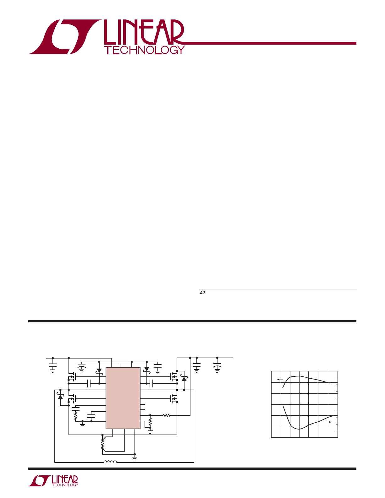
TYPICAL APPLICATION
High Effi ciency Buck-Boost Converter
V
IN
5V TO 32V
22μF
50V
CER
+
4.7μF
A
0.1μF 0.1μF
B
2200pF
20k
V
IN
TG2
BOOST2
SW2
BG2
I
TH
SS
0.1μF
SGND FCB
SENSE+SENSE–PGND
0.010Ω
4.7μH
PGOOD
LTC3780
INTV
BOOST1
SW1
PLLIN
RUN
V
OSENSE
CC
TG1
BG1
ON/OFF
7.5k
1%
1μF
CER
105k
1%
V
OUT
100μF
+
16V
D
C
CER
3780 TA01
330μF
16V
12V
5A
Effi ciency and Power Loss
V
= 12V, I
100
95
90
85
EFFICIENCY (%)
80
75
70
0
510
OUT
LOAD
20 30 35
15 25
VIN (V)
= 5A
3780 TA01b
10
9
8
POWER LOSS (W)
7
6
5
4
3
2
1
0
3780fe
1
Page 2
LTC3780
ABSOLUTE MAXIMUM RATINGS
(Note 1)
Input Supply Voltage (VIN) ........................ –0.3V to 36V
Topside Driver Voltages
(BOOST1, BOOST2) .................................. –0.3V to 42V
Switch Voltage (SW1, SW2) ........................ –5V to 36V
INTV
, EXTVCC, (BOOST – SW1),
CC
(BOOST2 – SW2), PGOOD .......................... –0.3V to 7V
RUN, SS ....................................................... –0.3V to 6V
PLLIN Voltage .......................................... –0.3V to 5.5V
PLLFLTR Voltage ....................................... –0.3V to 2.7V
FCB, STBYMD Voltages ........................ –0.3V to INTV
ITH, V
OSENSE
Voltages .............................. –0.3V to 2.4V
CC
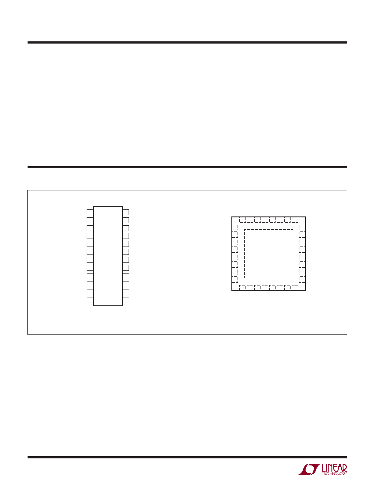
PIN CONFIGURATION
TOP VIEW
PGOOD
SENSE
SENSE
I
V
OSENSE
SGND
RUN
FCB
PLLFLTR
PLLIN
STBYMD
1
2
SS
+
3
–
4
5
TH
6
7
8
9
10
11
12
G PACKAGE
24-LEAD PLASTIC SSOP
T
= 125°C, θJA = 130°C/W
JMAX
24
23
22
21
20
19
18
17
16
15
14
13
BOOST1
TG1
SW1
V
IN
EXTV
CC
INTV
CC
BG1
PGND
BG2
SW2
TG2
BOOST2
Peak Output Current <10μs (TG1, TG2, BG1, BG2) .....3A
INTV
Peak Output Current ................................. 40mA
CC
Operating Junction Temperature Range (Notes 5, 2, 7)
LTC3780E ............................................. –40°C to 85°C
LTC3780I............................................ –40°C to 125°C
LTC3780MP ....................................... –55°C to 125°C
Junction Temperature (Note 2) ............................ 125°C
Storage Temperature Range ................... –65°C to 125°C
Lead Temperature (Soldering, 10 sec)
SSOP Only ........................................................ 300°C
TOP VIEW
NCSSPGOODNCNC
32 31 30 29 28 27 26 25
+
1SENSE
–
SENSE
2
I
3
TH
V
4
OSENSE
SGND
5
RUN
6
FCB
7
PLLFTR
8
9 10 11 12
NC
PLLIN
STBYMD
32-LEAD (5mm s 5mm) PLASTIC QFN
EXPOSED PAD (PIN 33) IS GND, MUST BE SOLDERED TO PCB
UH PACKAGE
T
= 125°C, θJA = 34°C/W
JMAX
BOOST1
33
13 14 15 16
NC
NC
BOOST2
TG1
TG2
NC
NC
24
SW1
V
23
IN
EXTV
22
CC
INTV
21
CC
BG1
20
PGND
19
BG2
18
SW2
17
2
3780fe
Page 3
LTC3780
ORDER INFORMATION
LEAD FREE FINISH TAPE AND REEL PART MARKING PACKAGE DESCRIPTION TEMPERATURE RANGE
LTC3780EG#PBF LTC3780EG#TRPBF LTC3780EG 24-Lead Plastic SSOP –40°C to 85°C
LTC3780IG#PBF LTC3780IG#TRPBF LTC3780IG 24-Lead Plastic SSOP –40°C to 125°C
LTC3780EUH#PBF LTC3780EUH#TRPBF 3780
LTC3780IUH#PBF LTC3780IUH#TRPBF 3780I
32-Lead (5mm × 5mm) Plastic QFN
32-Lead (5mm × 5mm) Plastic QFN
LEAD BASED FINISH TAPE AND REEL PART MARKING PACKAGE DESCRIPTION TEMPERATURE RANGE
LTC3780EG LTC3780EG#TR LTC3780EG 24-Lead Plastic SSOP –40°C to 85°C
LTC3780IG LTC3780IG#TR LTC3780IG 24-Lead Plastic SSOP –40°C to 125°C
LTC3780MPG LTC3780MPG#TR LTC3780MPG 24-Lead Plastic SSOP –55°C to 125°C
LTC3780EUH LTC3780EUH#TR 3780
LTC3780IUH LTC3780IUH#TR 3780I
32-Lead (5mm × 5mm) Plastic QFN
32-Lead (5mm × 5mm) Plastic QFN
Consult LTC Marketing for parts specifi ed with wider operating temperature ranges.
For more information on lead free part marking, go to:
For more information on tape and reel specifi cations, go to:
ELECTRICAL CHARACTERISTICS
The l denotes the specifi cations which apply over the full operating
http://www.linear.com/leadfree/
http://www.linear.com/tapeandreel/
junction temperature range, otherwise specifi cations are at TA = 25°C. VIN = 15V unless otherwise noted.
SYMBOL PARAMETER CONDITIONS MIN TYP MAX UNITS
Main Control Loop
V
OSENSE
Feedback Reference Voltage ITH = 1.2V, –40°C ≤ T ≤ 85°C (Note 3)
–55°C ≤ T ≤ 125°C
I
VOSENSE
V
LOADREG
V
REF(LINEREG)
g
m(EA)
g
m(GBW)
I
Q
Feedback Pin Input Current (Note 3) –5 –50 nA
Output Voltage Load Regulation (Note 3)
ΔI
= 1.2V to 0.7V
TH
ΔI
= 1.2V to 1.8V
TH
Reference Voltage Line Regulation VIN = 4V to 30V, ITH = 1.2V (Note 3) 0.002 0.02 %/V
Error Amplifi er Transconductance ITH = 1.2V, Sink/Source = 3μA (Note 3) 0.32 mS
Error Amplifi er GBW (Note 8) 0.6 MHz
Input DC Supply Current
(Note 4)
Normal
V
FCB
I
FCB
V
BINHIBIT
Standby
Shutdown Supply Current
Forced Continuous Threshold 0.76 0.800 0.84 V
Forced Continuous Pin Current V
Burst Inhibit (Constant Frequency)
V
= 0V, V
RUN
V
= 0V, V
RUN
= 0.85V –0.30 –0.18 –0.1 μA
FCB
Measured at FCB Pin 5.3 5.5 V
Threshold
UVLO Undervoltage Reset VIN Falling
V
OVL
I
SENSE
V
STBYMD(START)
V
STBYMD(KA)
Feedback Overvoltage Lockout Measured at V
Sense Pins Total Source Current V
Start-Up Threshold V
Keep-Alive Power-On Threshold V
SENSE
STBYMD
STBYMD
–
= V
> 2V
STBYMD
= Open
STBYMD
Pin 0.84 0.86 0.88 V
OSENSE
+
= 0V –380 μA
SENSE
Rising 0.4 0.7 V
Rising, V
= 0V 1.25 V
RUN
l
0.792
l
0.792
l
l
l
–40°C to 85°C
–40°C to 125°C
–40°C to 85°C
–40°C to 125°C
0.800
0.800
0.1
–0.1
0.808
0.811
0.5
–0.5
2400
1500
55 70
3.8 4 V
μA
μA
μA
V
V
%
%
3780fe
3
Page 4
LTC3780
ELECTRICAL CHARACTERISTICS
The l denotes the specifi cations which apply over the full operating
junction temperature range, otherwise specifi cations are at T
SYMBOL PARAMETER CONDITIONS MIN TYP MAX UNITS
DF MAX, Boost Maximum Duty Factor % Switch C On 99 %
DF MAX, Buck Maximum Duty Factor % Switch A On (in Dropout) 99 %
V
RUN(ON)
I
SS
V
SENSE(MAX)
V
SENSE(MIN,BUCK)
TG1, TG2 t
TG1, TG2 t
r
f
BG1, BG2 t
BG1, BG2 t
TG1/BG1 t
BG1/TG1 t
TG2/BG2 t
BG2/TG2 t
1D
2D
3D
4D
Mode
Transition 1
Mode
Transition 2
t
ON(MIN,BOOST)
t
ON(MIN,BUCK)
Internal VCC Regulator
V
INTVCC
ΔV
LDO(LOADREG)
V
EXTVCC
ΔV
EXTVCC(HYS)
ΔV
EXTVCC
Oscillator and Phase-Locked Loop
f
NOM
f
LOW
f
HIGH
R
PLLIN
I
PLLLPF
RUN Pin On Threshold V
Soft-Start Charge Current V
Maximum Current Sense Threshold Boost: V
Buck: V
Minimum Current Sense Threshold Discontinuous Mode –6 mV
TG Rise Time C
TG Fall Time C
BG Rise Time C
r
BG Fall Time C
f
TG1 Off to BG1 On Delay,
C
Switch C On Delay
BG1 Off to TG1 On Delay,
C
Synchronous Switch D On Delay
TG2 Off to BG2 On Delay,
C
Synchronous Switch B On Delay
BG2 Off to TG2 On Delay,
C
Switch A On Delay
BG1 Off to BG2 On Delay,
C
Switch A On Delay
BG2 Off to BG1 On Delay,
C
Synchronous Switch D On Delay
Minimum On-Time for Main Switch in
Switch C (Note 6) 200 ns
Boost Operation
Minimum On-Time for Synchronous
Switch B (Note 6) 180 ns
Switch in Buck Operation
Internal VCC Voltage 7V < VIN < 30V, V
Internal VCC Load Regulation ICC = 0mA to 20mA, V
EXTVCC Switchover Voltage ICC = 20mA, V
EXTVCC Switchover Hysteresis 300 mV
EXTVCC Switch Drop Voltage ICC = 20mA, V
Nominal Frequency V
Lowest Frequency V
Highest Frequency V
PLLIN Input Resistance 50 kΩ
Phase Detector Output Current f
f
= 25°C. VIN = 15V unless otherwise noted.
A
Rising 1 1.5 2 V
RUN
= 2V 0.5 1.2 μA
RUN
= V
OSENSE
OSENSE
= 3300pF (Note 5) 50 ns
LOAD
= 3300pF (Note 5) 45 ns
LOAD
= 3300pF (Note 5) 45 ns
LOAD
= 3300pF (Note 5) 55 ns
LOAD
= 3300pF Each Driver 80 ns
LOAD
= 3300pF Each Driver 80 ns
LOAD
= 3300pF Each Driver 80 ns
LOAD
= 3300pF Each Driver 80 ns
LOAD
= 3300pF Each Driver 250 ns
LOAD
= 3300pF Each Driver 250 ns
LOAD
= 1.2V 260 300 330 kHz
PLLFLTR
= 0V 170 200 220 kHz
PLLFLTR
= 2.4V 340 400 440 kHz
PLLFLTR
< f
PLLIN
OSC
> f
OSC
(Note 9)
PLLIN
– 50mV
REF
= V
– 50mV
REF
= 5V
EXTVCC
= 5V 0.2 2 %
EXTVCC
Rising
EXTVCC
= 6V 150 300 mV
EXTVCC
l
l
–95
l
5.7 6 6.3 V
l
5.4 5.7 V
160
–110
185
–150
–15
15
mV
mV
μA
μA
4
3780fe
Page 5
LTC3780
ELECTRICAL CHARACTERISTICS
The l denotes the specifi cations which apply over the full operating
junction temperature range, otherwise specifi cations are at T
SYMBOL PARAMETER CONDITIONS MIN TYP MAX UNITS
PGOOD Output
ΔV
FBH
ΔV
FBL
ΔV
FB(HYST)
V
PGL
I
PGOOD
Note 1: Stresses beyond those listed under Absolute Maximum Ratings
may cause permanent damage to the device. Exposure to any Absolute
Maximum Rating condition for extended periods may affect device
reliability and lifetime.
Note 2: T
power dissipation P
T
Note 3: The IC is tested in a feedback loop that servos V
voltage and measures the resultant V
Note 4: Dynamic supply current is higher due to the gate charge being
delivered at the switching frequency.
Note 5: Rise and fall times are measured using 10% and 90% levels. Delay
times are measured using 50% levels.
for the QFN package is calculated from the temperature TA and
J
= TA + (PD • 34°C/W)
J
PGOOD Upper Threshold V
PGOOD Lower Threshold V
PGOOD Hysteresis V
PGOOD Low Voltage I
PGOOD Leakage Current V
according to the following formula:
D
to a specifi ed
ITH
OSENSE
.
= 25°C. VIN = 15V unless otherwise noted.
A
Rising 5.5 7.5 10 %
OSENSE
Falling –5.5 –7.5 –10 %
OSENSE
Returning 2.5 %
OSENSE
= 2mA 0.1 0.3 V
PGOOD
= 5V ±1 μA
PGOOD
Note 6: The minimum on-time condition is specifi ed for an inductor
peak-to-peak ripple current ≥ 40% of I
considerations in the Applications Information section).
Note 7: The LTC3780E is guaranteed to meet performance specifi cations
from 0°C to 85°C. Performance over the –40°C to 85°C operating junction
temperature range is assured by design, characterization and correlation
with statistical process controls. The LTC3780I is guaranteed over the
–40°C to 125°C operating junction temperature range. The LTC3780MP
is guaranteed and tested over the full –55 to 125°C operating junction
temperature range.
Note 8: This parameter is guaranteed by design.
Note 9: f
is the running frequency for the application.
OSC
(see minimum on-time
MAX
3780fe
5
Page 6
LTC3780
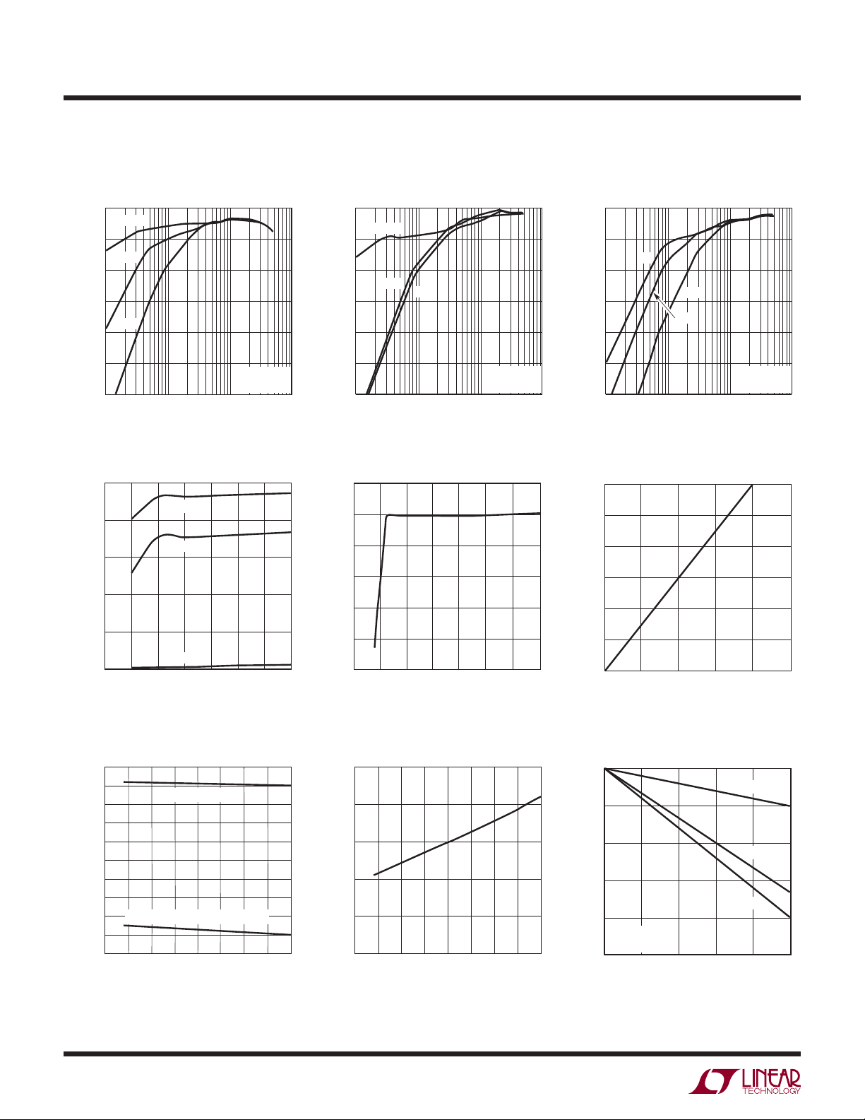
TYPICAL PERFORMANCE CHARACTERISTICS
Effi ciency vs Output Current
(Boost Operation)
100
BURST
90
DCM
80
70
CCM
EFFICIENCY (%)
60
50
40
0.01
VIN = 6V
= 12V
V
OUT
0.1 1 10
I
(A)
LOAD
3780 G01
Effi ciency vs Output Current
100
BURST
90
80
DCM
70
EFFICIENCY (%)
60
50
40
0.01
CCM
0.1 1 10
I
LOAD
(A)
T
= 25°C unless othewise noted.
A
Effi ciency vs Output Current
(Buck Operation)
100
90
80
70
EFFICIENCY (%)
60
VIN = 12V
= 12V
V
OUT
3780 G02
50
40
0.01
Supply Current vs Input Voltage Internal 6V LDO Line Regulation EXTVCC Voltage Drop
2500
2000
V
= 0V
FCB
6.5
6.0
120
100
SC
CCM
DCM
VIN = 18V
V
0.1 1 10
I
(A)
LOAD
OUT
= 12V
3780 G03
1500
1000
SUPPLY CURRENT (μA)
500
0
05
INTV
STANDBY
SHUTDOWN
10
INPUT VOLTAGE (V)
and EXTVCC Switch
CC
Voltage vs Temperature
6.05
6.00
5.95
5.90
5.85
5.80
SWITCH VOLTAGE (V)
CC
5.75
5.70
AND EXTV
5.65
CC
5.60
INTV
5.55
–75 –50
INTVCC VOLTAGE
EXTVCC SWITCHOVER THRESHOLD
–25
TEMPERATURE (°C)
5.5
5.0
VOLTAGE (V)
CC
4.5
INTV
4.0
20
15
25
30
35
3780 G04
3.5
0
510
INPUT VOLTAGE (V)
20 30 35
15 25
3780 G05
80
60
VOLTAGE DROP (mV)
40
CC
EXTV
20
0
0
10 20 30 40
CURRENT (mA)
50
3780 G06
EXTVCC Switch Resistance
vs Temperature
5
4
3
2
SWITCH RESISTANCE (Ω)
CC
1
EXTV
0
75
50
25
100
125
3780 G07
0
–75 –50 –25
50
25
0
TEMPERATURE (°C)
100
125
3780 G08
75
Load Regulation
0
–0.1
(%)
OUT
–0.2
–0.3
NORMALIZED V
–0.4
FCB = 0V
= 12V
V
OUT
–0.5
0
1
2
LOAD CURRENT (A)
3
VIN = 18V
VIN = 12V
VIN = 6V
4
5
3780 G09
6
3780fe
Page 7
LTC3780
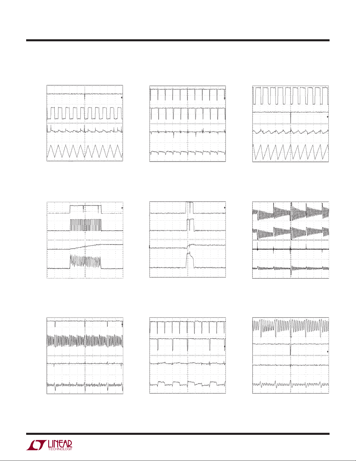
TYPICAL PERFORMANCE CHARACTERISTICS
SW2
10V/DIV
SW1
10V/DIV
V
OUT
100mV/DIV
2A/DIV
SW2
10V/DIV
SW1
10V/DIV
V
OUT
500mV/DIV
2A/DIV
Continuous Current Mode
(CCM, VIN = 6V, V
I
L
= 6V
IN
= 12V
V
OUT
= 12V)
OUT
5μs/DIVV
Burst Mode Operation
(VIN = 6V, V
I
L
OUT
= 12V)
100mV/DIV
3780 G10
200mV/DIV
Continuous Current Mode
(CCM, VIN = 12V, V
SW2
10V/DIV
SW1
10V/DIV
V
OUT
I
L
2A/DIV
= 12V
IN
= 12V
V
OUT
Burst Mode Operation
(VIN = 12V, V
SW2
10V/DIV
SW1
10V/DIV
V
OUT
I
L
2A/DIV
5μs/DIVV
OUT
OUT
= 12V)
= 12V)
TA = 25°C unless othewise noted.
Continuous Current Mode
(CCM, VIN = 18V, V
SW2
10V/DIV
SW1
10V/DIV
V
OUT
100mV/DIV
I
L
2A/DIV
3780 G11
= 18V
IN
= 12V
V
OUT
5μs/DIVV
Skip-Cycle Mode
SW2
10V/DIV
SW1
10V/DIV
V
OUT
100mV/DIV
1A/DIV
(VIN = 18V, V
I
L
OUT
OUT
= 12V)
= 12V)
3780 G12
SW2
10V/DIV
SW1
10V/DIV
V
OUT
100mV/DIV
1A/DIV
= 6V
IN
= 12V
V
OUT
25μs/DIVV
Discontinuous Current Mode
(DCM, VIN = 6V, V
I
L
= 6V
IN
= 12V
V
OUT
= 12V)
OUT
5μs/DIVV
3780 G13
3780 G16
SW2
10V/DIV
SW1
10V/DIV
V
OUT
100mV/DIV
2A/DIV
= 12V
IN
= 12V
V
OUT
10μs/DIVV
Discontinuous Current Mode
(DCM, VIN = 12V, V
I
L
= 12V
IN
= 12V
V
OUT
5μs/DIVV
OUT
= 12V)
3780 G14
3780 G17
SW2
10V/DIV
SW1
10V/DIV
V
OUT
100mV/DIV
1A/DIV
V
IN
OUT
= 18V
= 12V
2.5μs/DIVV
Discontinuous Current Mode
(DCM, VIN = 18V, V
I
L
= 18V
IN
= 12V
V
OUT
2.5μs/DIVV
OUT
= 12V)
3780 G15
3780 G18
3780fe
7
Page 8
LTC3780
TYPICAL PERFORMANCE CHARACTERISTICS
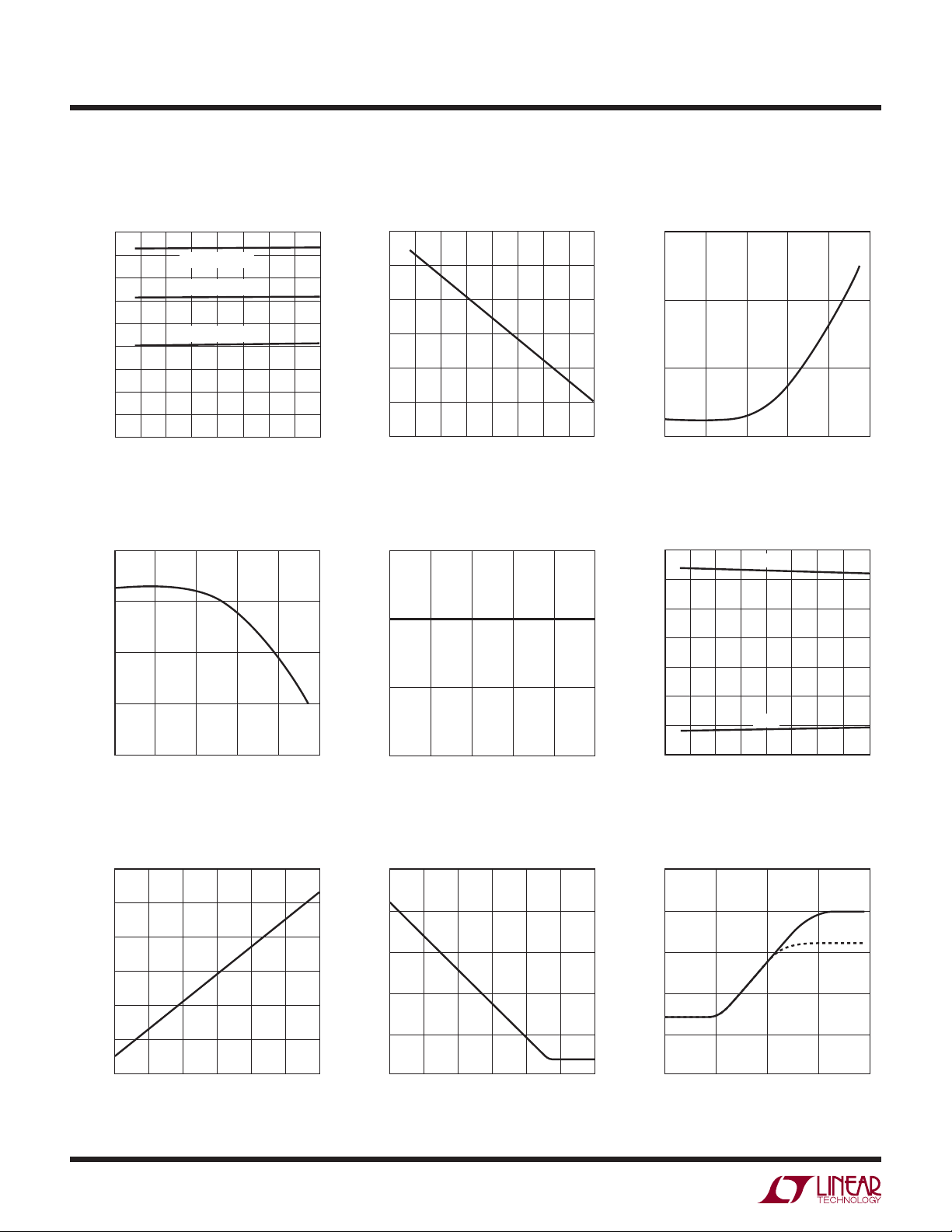
Oscillator Frequency
vs Temperature
450
400
350
300
250
200
150
FREQUENCY (kHz)
100
50
0
–75 –50
V
PLLFLTR
V
PLLFLTR
V
PLLFLTR
0
–25
25 125
TEMPERATURE (°C)
= 2.4V
= 1.2V
= 0V
50
Maximum Current Sense
Threshold vs Duty Factor (Boost)
180
160
(mV)
+
140
SENSE
I
120
100
20
0
DUTY FACTOR (%)
60
40
75 100
80
3780 G19
100
3780 G22
Undervoltage Reset
vs Temperature
4.2
4.0
3.8
3.6
3.4
UNDERVOLTAGE RESET (V)
3.2
3.0
–75 –50 –25
0
TEMPERATURE (°C)
50
25
Maximum Current Sense
Threshold vs Duty Factor (Buck)
140
130
(mV)
+
SNESE
I
120
110
20 40 60 80
DUTY FACTOR (%)
75
TA = 25°C unless othewise noted.
Minimum Current Sense
Threshold vs Duty Factor (Buck)
–20
–40
(mV)
+
SENSE
I
–60
100
125
3780 G20
–80
80 60 40 20
DUTY FACTOR (%)
Minimum Current Sense
Threshold vs Temperature
3780 G23
200
150
100
50
THRESHOLD (mV)
+
0
SNESE
–50
–100
MAXIMUM I
–150
1000
–75 –50
BOOST
BUCK
–25 0
TEMPERATURE (°C)
50 100 125
25 75
0100
3780 G21
3780 G24
Peak Current Threshold
vs V
(Boost)
ITH
50
0
0
0.4
(mV)
+
SENSE
I
–100
200
150
100
–50
8
0.8 1.2 1.6
V
(V)
ITH
1.8 2.4
3780 G25
Valley Current Threshold
vs V
(Buck)
ITH
50
0
0
0.8 1.2 1.6
0.4
(mV)
+
SENSE
I
–100
–150
100
–50
Current Foldback Limit
200
160
120
(mV)
+
SENSE
80
I
40
V
(V)
ITH
2.0 2.4
3780 G26
0
0
0.2 0.4 0.6
V
(V)
OSENSE
BOOST
BUCK
0.8
3780 G32
3780fe
Page 9
LTC3780
TYPICAL PERFORMANCE CHARACTERISTICS
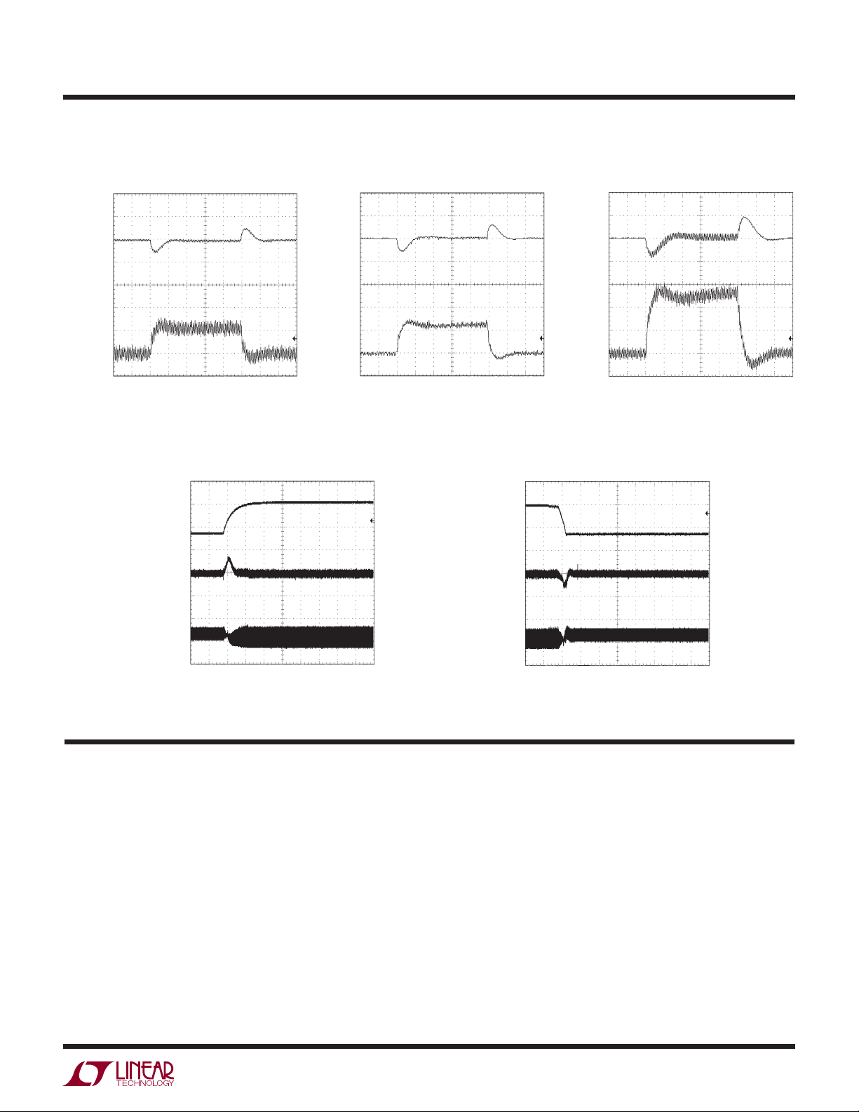
Load Step Load Step Load Step
V
OUT
500mV/DIV
5A/DIV
I
L
= 12V
V
OUT
LOAD STEP: 0A TO 5A
CONTINUOUS MODE
10V/DIV
200μs/DIVVIN = 18V
3780 G27
Line Transient Line Transient
V
IN
V
OUT
500mV/DIV
5A/DIV
I
L
= 12V
IN
= 12V
V
OUT
LOAD STEP: 0A TO 5A
CONTINUOUS MODE
200μs/DIVV
10V/DIV
TA = 25°C unless othewise noted.
V
OUT
500mV/DIV
I
L
5A/DIV
3780 G28
V
IN
= 6V
IN
= 12V
V
OUT
LOAD STEP: 0A TO 5A
CONTINUOUS MODE
200μs/DIVV
3780 G29
V
OUT
500mV/DIV
I
L
1A/DIV
OUT
I
LOAD
STEP: 7V TO 20V
V
IN
CONTINUOUS MODE
PIN FUNCTIONS
= 12V
= 1A
(SSOP/QFN)
500μs/DIVV
3780 G30
PGOOD (Pin 1/Pin 30): Open-Drain Logic Output. PGOOD
is pulled to ground when the output voltage is not within
±7.5% of the regulation point.
SS (Pin 2/Pin 31): Soft-start reduces the input power
sources’ surge currents by gradually increasing the
controller’s current limit. A minimum value of 6.8nF is
recommended on this pin.
+
SENSE
and Reverse Current Detect Comparators. The I
(Pin 3/Pin 1): The (+) Input to the Current Sense
pin
TH
V
OUT
500mV/DIV
I
L
1A/DIV
= 12V
OUT
= 1A
I
LOAD
STEP: 20V TO 7V
V
IN
CONTINUOUS MODE
500μs/DIVV
voltage and built-in offsets between SENSE
pins, in conjunction with R
SENSE
3780 G31
–
and SENSE+
, set the current trip
threshold.
–
SENSE
(Pin 4/Pin 2): The (–) Input to the Current Sense
and Reverse Current Detect Comparators.
(Pin 5/Pin 3): Current Control Threshold and Error
I
TH
Amplifi er Compensation Point. The current comparator
threshold increases with this control voltage. The voltage
ranges from 0V to 2.4V.
3780fe
9
Page 10

LTC3780
PIN FUNCTIONS
V
OSENSE
(Pin 6/Pin 4): Error Amplifi er Feedback Input.
(SSOP/QFN)
This pin connects the error amplifi er input to an external
resistor divider from V
OUT
.
SGND (Pin 7/Pin 5): Signal Ground. All small-signal components and compensation components should connect
to this ground, which should be connected to PGND at a
single point.
RUN (Pin 8/Pin 6): Run Control Input. Forcing the RUN
pin below 1.5V causes the IC to shut down the switching
regulator circuitry. There is a 100k resistor between the RUN
pin and SGND in the IC. Do not apply >6V to this pin.
FCB (Pin 9/Pin 7): Forced Continuous Control Input. The
voltage applied to this pin sets the operating mode of the
controller. When the applied voltage is less than 0.8V, the
forced continuous current mode is active. When this pin
is allowed to fl oat, the Burst Mode operation is active in
boost operation and the skip-cycle mode is active in buck
operation. When the pin is tied to INTV
, the constant
CC
frequency discontinuous current mode is active in buck
or boost operation.
PLLFLTR (Pin 10/Pin 8): The phase-locked loop’s
lowpass fi lter is tied to this pin. Alternatively, this pin can
be driven with an AC or DC voltage source to vary the
frequency of the internal oscillator.
PLLIN (Pin 11/Pin 10): External Synchronization Input to
Phase Detector. This pin is internally terminated to SGND
with 50kΩ. The phase-locked loop will force the rising
bottom gate signal of the controller to be synchronized
with the rising edge of the PLLIN signal.
STBYMD (Pin 12/Pin 11): LDO Control Pin. Determines
whether the internal LDO remains active when the controller is shut down. See Operation section for details. If the
STBYMD pin is pulled to ground, the SS pin is internally
pulled to ground, preventing start-up and thereby providing a single control pin for turning off the controller. To
keep the LDO active when RUN is low, for example to
power a “wake up” circuit which controls the state of the
RUN pin, bypass STBYMD to signal ground with a 0.1μF
capacitor, or use a resistor divider from V
to keep the
IN
pin within 2V to 5V.
BOOST2, BOOST1 (Pins 13, 24/Pins 14, 27): Boosted
Floating Driver Supply. The (+) terminal of the bootstrap
capacitor C
pin swings from a diode voltage below INTV
+ INTV
below INTV
and CB (Figure 11) connects here. The BOOST2
A
up to VIN
CC
. The BOOST1 pin swings from a diode voltage
CC
up to V
CC
+ INTVCC.
OUT
TG2, TG1 (Pins 14, 23/Pins 15, 26): Top Gate Drive. Drives
the top N-channel MOSFET with a voltage swing equal to
INTV
superimposed on the switch node voltage SW.
CC
SW2, SW1 (Pins 15, 22/Pins 17, 24): Switch Node. The (–)
terminal of the bootstrap capacitor C
and CB (Figure 11)
A
connects here. The SW2 pin swings from a Schottky diode
(external) voltage drop below ground up to V
. The SW1
IN
pin swings from a Schottky diode (external) voltage drop
below ground up to V
OUT
.
BG2, BG1 (Pins 16, 18/Pins 18, 20): Bottom Gate Drive.
Drives the gate of the bottom N-channel MOSFET between
ground and INTV
CC
.
PGND (Pin 17/Pin 19): Power Ground. Connect this pin
closely to the source of the bottom N-channel MOSFET, the
(–) terminal of C
INTV
(Pin 19/Pin 21): Internal 6V Regulator Output. The
CC
and the (–) terminal of CIN (Figure 11).
VCC
driver and control circuits are powered from this voltage.
Bypass this pin to ground with a minimum of 4.7μF low
ESR tantalum or ceramic capacitor.
EXTV
exceeds 5.7V, an internal switch connects this pin to INTV
(Pin 20/Pin 22): External VCC Input. When EXTVCC
CC
CC
and shuts down the internal regulator so that the controller
and gate drive power is drawn from EXTV
7V at this pin and ensure that EXTV
(Pin 21/Pin 23): Main Input Supply. Bypass this pin
V
IN
. Do not exceed
CC
< VIN.
CC
to SGND with an RC fi lter (1Ω, 0.1μF).
Exposed Pad (Pin 33, QFN Only): This pin is SGND and
must be soldered to PCB ground.
10
3780fe
Page 11
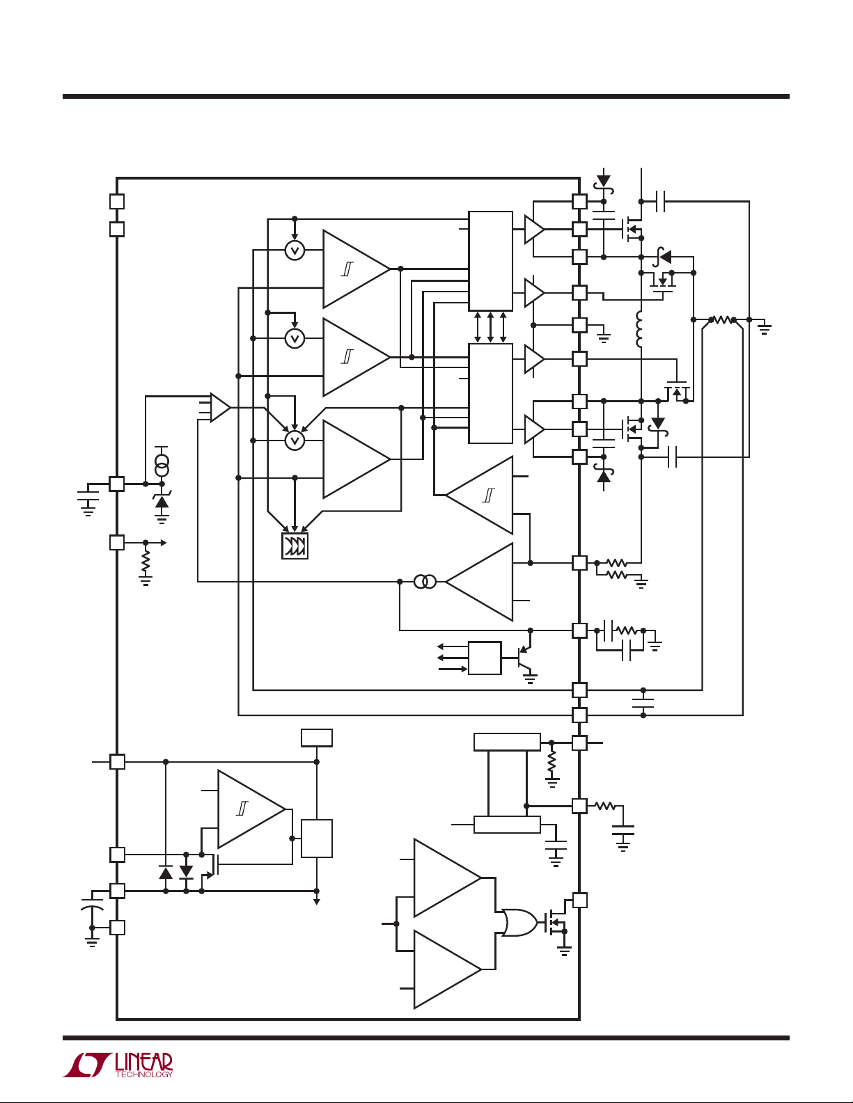
BLOCK DIAGRAM
INTV
LTC3780
CCVIN
STBYMD
FCB
SS
RUN
100k
1.2V
4(V
1.2μA
BOOST2
INTV
CC
TG2
SW2
BG2
PGND
R
SENSE
I
LIM
+
FCB
BUCK
LOGIC
–
I
REV
+
BG1
–
)
FB
I
CMP
+
–
SLOPE
FCB
OV
EA
BOOST
LOGIC
INTV
CC
SW1
TG1
BOOST1
0.86V
–
INTV
CC
V
+
V
OSENSE
–
V
FB
OUT
0.80V
+
I
TH
SHDN
RST
4(V
FB
V
V
V
IN
IN
5.7V
+
–
EXTV
CC
INTV
6V
+
CC
SGND
REF
6V
LDO
REG
INTERNAL
SUPPLY
V
OSENSE
0.86V
–
+
RUN/
CLK
SS
PHASE DET
OSCILLATOR
SENSE
SENSE
PLLIN
PLLFLTR
PGOOD
50k
+
–
F
IN
R
LP
C
LP
)
–
0.74V
+
3780 BD
3780fe
11
Page 12
LTC3780
OPERATION
MAIN CONTROL LOOP
The LTC3780 is a current mode controller that provides an
output voltage above, equal to or below the input voltage.
The LTC proprietary topology and control architecture employs a current-sensing resistor in buck or boost modes.
The sensed inductor current is controlled by the voltage
on the I
V
OSENSE
pin, which is the output of the amplifi er EA. The
TH
pin receives the voltage feedback signal, which is
compared to the internal reference voltage by the EA.
The top MOSFET drivers are biased from fl oating booststrap capacitors C
and CB (Figure 11), which are normally
A
recharged through an external diode when the top MOSFET
is turned off. Schottky diodes across the synchronous
switch D and synchronous switch B are not required, but
provide a lower drop during the dead time. The addition of
the Schottky diodes will typically improve peak effi ciency
by 1% to 2% at 400kHz.
The main control loop is shut down by pulling the RUN
pin low. When the RUN pin voltage is higher than 1.5V, an
internal 1.2μA current source charges soft-start capacitor
at the SS pin. The ITH voltage is then clamped to the
C
SS
SS voltage while C
is slowly charged during start-up.
SS
This “soft-start” clamping prevents abrupt current from
being drawn from the input power supply.
POWER SWITCH CONTROL
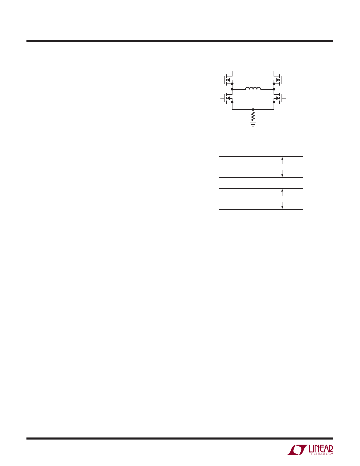
Figure 1 shows a simplifi ed diagram of how the four
, V
power switches are connected to the inductor, V
IN
OUT
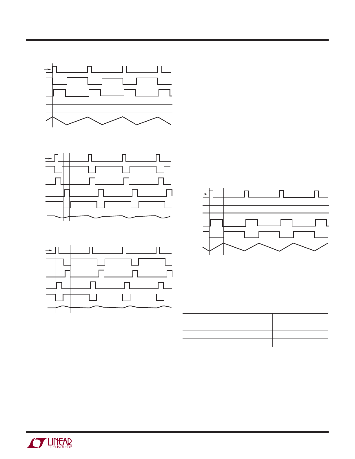
and GND. Figure 2 shows the regions of operation for the
LTC3780 as a function of duty cycle D. The power switches
are properly controlled so the transfer between modes is
continuous. When V
approaches V
IN
, the buck-boost
OUT
region is reached; the mode-to-mode transition time is
typically 200ns.
V
IN
TG2
BG2
Figure 1. Simplifi ed Diagram of the Output Switches
98%
D
MAX
BOOST
D
MIN
BOOST
D
MAX
BUCK
3%
D
MIN
BUCK
Figure 2. Operating Mode vs Duty Cycle
A
B
A ON, B OFF
PWM C, D SWITCHES
FOUR SWITCH PWM
D ON, C OFF
PWM A, B SWITCHES
L
SW2 SW1
V
OUT
D
C
R
SENSE
3780 F01
BOOST REGION
BUCK/BOOST REGION
BUCK REGION
TG1
BG1
3780 F02
and switch A is turned on for the remainder of the cycle.
switches A and B will alternate, behaving like a typical
synchronous buck regulator. The duty cycle of switch A
increases until the maximum duty cycle of the converter
in buck mode reaches D
D
MAX_BUCK
where D
= 100% – D
BUCK-BOOST
= duty cycle of the buck-boost switch
MAX_BUCK
BUCK-BOOST
, given by:
range:
D
BUCK-BOOST
= (200ns • f) • 100%
and f is the operating frequency in Hz.
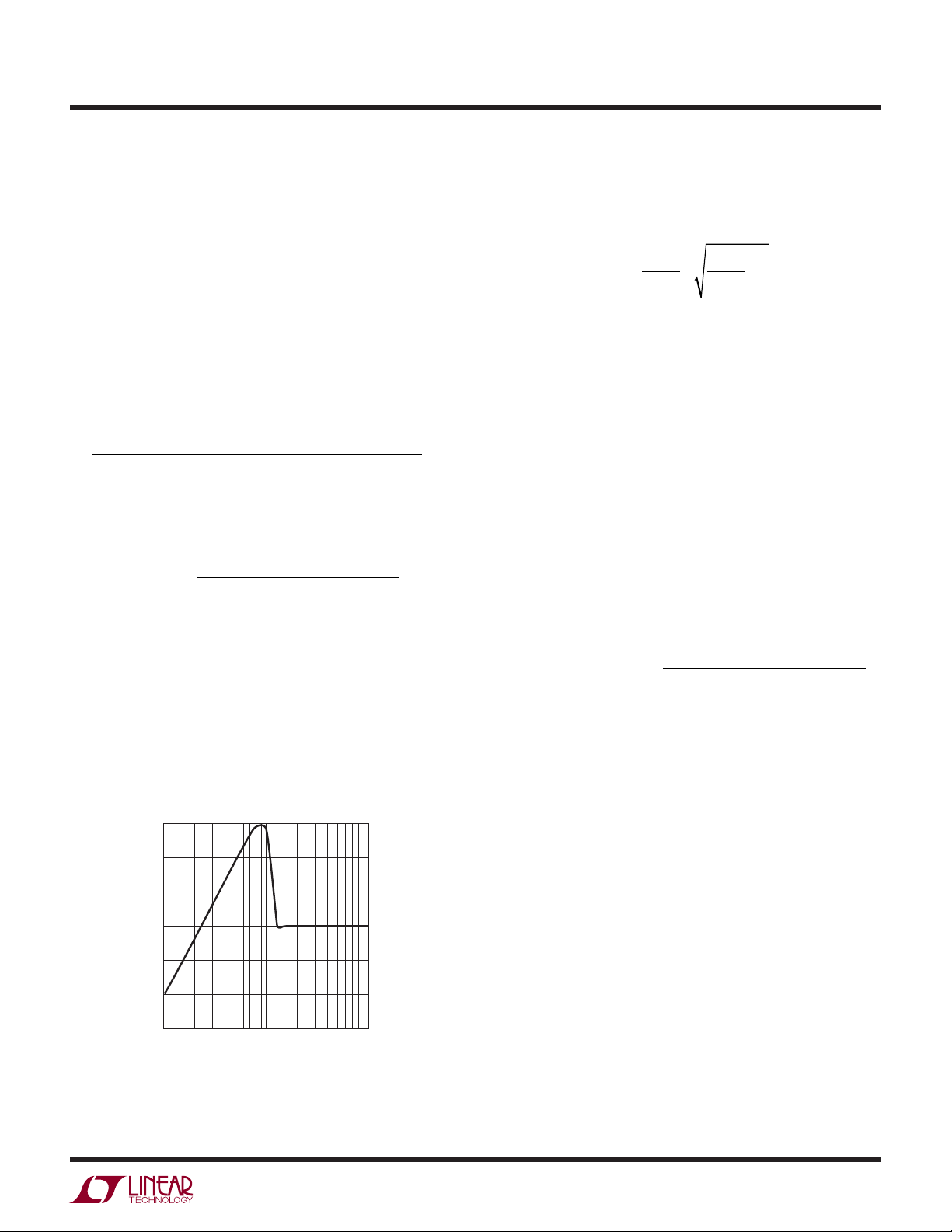
Figure 3 shows typical buck mode waveforms. If V
approaches V
, the buck-boost region is reached.
OUT
IN
Buck Region (V
IN
> V
OUT
)
Switch D is always on and switch C is always off during
this mode. At the start of every cycle, synchronous switch
B is turned on fi rst. Inductor current is sensed when
synchronous switch B is turned on. After the sensed inductor current falls below the reference voltage, which is
proportional to V
, synchronous switch B is turned off
ITH
12
Buck-Boost (V
When V
is close to V
IN
IN
≅ V
)
OUT
, the controller is in buck-boost
OUT
mode. Figure 4 shows typical waveforms in this mode.
Every cycle, if the controller starts with switches B and D
turned on, switches A and C are then turned on. Finally,
switches A and D are turned on for the remainder of the
time. If the controller starts with switches A and C turned
3780fe
Page 13
OPERATION
LTC3780
CLOCK
SWITCH A
SWITCH B
SWITCH C
SWITCH D
CLOCK
SWITCH A
SWITCH B
SWITCH C
SWITCH D
the remainder of the cycle. switches C and D will alternate,
behaving like a typical synchronous boost regulator.
The duty cycle of switch C decreases until the minimum duty
cycle of the converter in boost mode reaches D
0V
given by:
HIGH
I
L
Figure 3. Buck Mode (VIN > V
OUT
)
3780 F03
D
MIN_BOOST
where D
switch range:
D
BUCK-BOOST
= D
BUCK-BOOST
= (200ns • f) • 100%
BUCK-BOOST
is the duty cycle of the buck-boost
MIN_BOOST
,
and f is the operating frequency in Hz.
Figure 5 shows typical boost mode waveforms. If V
proaches V
CLOCK
SWITCH A
I
L
3780 F04a
(4a) Buck-Boost Mode (VIN ≥ V
OUT
)
SWITCH B
SWITCH C
SWITCH D
, the buck-boost region is reached.
OUT
IN
ap-
HIGH
0V
CLOCK
SWITCH A
SWITCH B
SWITCH C
SWITCH D
I
L
(4b) Buck-Boost Mode (VIN ≤ V
OUT
)
3780 F04b
Figure 4. Buck-Boost Mode
on, switches B and D are then turned on. Finally, switches
A and D are turned on for the remainder of the time.
Boost Region (V
IN
< V
OUT
)
Switch A is always on and synchronous switch B is always
off in boost mode. Every cycle, switch C is turned on fi rst.
Inductor current is sensed when synchronous switch C is
turned on. After the sensed inductor current exceeds the
reference voltage which is proportional to V
, switch C
ITH
is turned off and synchronous switch D is turned on for
I
L
Figure 5. Boost Mode (VIN < V
OUT
)
3780 F05
LOW CURRENT OPERATION
The FCB pin is used to select among three modes for both
buck and boost operations by accepting a logic input.
Figure 6 shows the different modes.
FCB PIN BUCK MODE BOOST MODE
0V to 0.75V Force Continuous Mode Force Continuous Mode
0.85V to 5V Skip-Cycle Mode Burst Mode Operation
>5.3V DCM with Constant Freq DCM with Constant Freq
Figure 6. Different Operating Modes
When the FCB pin voltage is lower than 0.8V, the controller
behaves as a continuous, PWM current mode synchronous
switching regulator. In boost mode, switch A is always on.
switch C and synchronous switch D are alternately turned
on to maintain the output voltage independent of direction
of inductor current. Every ten cycles, switch A is forced off
for about 300ns to allow boost capacitor C
(Figure 13) to
A
recharge. In buck mode, synchronous switch D is always
3780fe
13
Page 14

LTC3780
OPERATION
on. switch A and synchronous switch B are alternately
turned on to maintain the output voltage independent of
direction of inductor current. Every ten cycles, synchronous switch D is forced off for about 300ns to allow C
B
to recharge. This is the least effi cient operating mode at
light load, but may be desirable in certain applications. In
this mode, the output can source or sink current.
When the FCB pin voltage is below V
– 1V, but greater
INTVCC
than 0.8V, the controller enters Burst Mode operation in
boost operation or enters skip-cycle mode in buck operation. During boost operation, Burst Mode operation sets a
minimum output current level before inhibiting the switch
C and turns off synchronous switch D when the inductor
current goes negative. This combination of requirements
will, at low currents, force the I
pin below a voltage
TH
threshold that will temporarily inhibit turn-on of power
switches C and D until the output voltage drops. There is
100mV of hysteresis in the burst comparator tied to the
pin. This hysteresis produces output signals to the
I
TH
MOSFETs C and D that turn them on for several cycles,
followed by a variable “sleep” interval depending upon the
load current. The maximum output voltage ripple is limited
to 3% of the nominal DC output voltage as determined
by a resistive feedback divider. During buck operation at
no load, switch A is turned on for its minimum on-time.
This will not occur every clock cycle when the output load
current drops below 1% of the maximum designed load.
The body diode of synchronous switch B or the Schottky
diode, which is in parallel with switch B, is used to discharge the inductor current; switch B only turns on every
ten clock cycles to allow C
to recharge. As load current
B
is applied, switch A turns on every cycle, and its on-time
begins to increase. At higher current, switch B turns on
briefl y after each turn-off of switch A. switches C and D
remain off at light load, except to refresh CA (Figure 11)
every 10 clock cycles. In Burst Mode operation/skip-cycle
mode, the output is prevented from sinking current.
When the FCB pin voltage is tied to the INTV
pin, the
CC
controller enters constant frequency discontinuous current
mode (DCM). For boost operation, synchronous switch D
is held off whenever the I
pin is below a threshold volt-
TH
age. In every cycle, switch C is used to charge inductor
current. After the output voltage is high enough, the
controller will enter continuous current buck mode for
one cycle to discharge inductor current. In the following
cycle, the controller will resume DCM boost operation. For
buck operation, constant frequency discontinuous current
mode sets a minimum negative inductor current level.
synchronous switch B is turned off whenever inductor
current is lower than this level. At very light loads, this
constant frequency operation is not as effi cient as Burst
Mode operation or skip-cycle, but does provide lower
noise, constant frequency operation.
FREQUENCY SYNCHRONIZATION AND
FREQUENCY SETUP
The phase-locked loop allows the internal oscillator to be
synchronized to an external source via the PLLIN pin. The
phase detector output at the PLLFLTR pin is also the DC
frequency control input of the oscillator. The frequency
ranges from 200kHz to 400kHz, corresponding to a DC
voltage input from 0V to 2.4V at PLLFLTR. When locked,
the PLL aligns the turn on of the top MOSFET to the rising edge of the synchronizing signal. When PLLIN is left
open, the PLLFLTR pin goes low, forcing the oscillator to
its minimum frequency.
INTV
/EXTVCC Power
CC
Power for all power MOSFET drivers and most internal circuitry is derived from the INTV
EXTV
regulator supplies INTV
pin is left open, an internal 6V low dropout linear
CC
power. If EXTVCC is taken above
CC
pin. When the
CC
5.7V, the 6V regulator is turned off and an internal switch
is turned on, connecting EXTV
the INTV
power to be derived from a high effi ciency
CC
to INTVCC. This allows
CC
external source.
POWER GOOD (PGOOD) PIN
The PGOOD pin is connected to an open drain of an internal
MOSFET. The MOSFET turns on and pulls the pin low when
the output is not within ±7.5% of the nominal output level
as determined by the resistive feedback divider. When
the output meets the ±7.5% requirement, the MOSFET
is turned off and the pin is allowed to be pulled up by an
external resistor to a source of up to 7V.
14
3780fe
Page 15

OPERATION
LTC3780
FOLDBACK CURRENT
Foldback current limiting is activated when the output
voltage falls below 70% of its nominal level, reducing
power waste. During start-up, foldback current limiting
is disabled.
INPUT UNDERVOLTAGE RESET
The SS capacitor will be reset if the input voltage is allowed to fall below approximately 4V. The SS capacitor
will attempt to charge through a normal soft-start ramp
after the input voltage rises above 4V.
OUTPUT OVERVOLTAGE PROTECTION
An overvoltage comparator guards against transient overshoots (>7.5%) as well as other more serious conditions
that may overvoltage the output. In this case, synchronous
switch B and synchronous switch D are turned on until the
overvoltage condition is cleared or the maximum negative
current limit is reached. When inductor current is lower
than the maximum negative current limit, synchronous
switch B and synchronous switch D are turned off, and
switch A and switch C are turned on until the inductor
current reaches another negative current limit. If the
comparator still detects an overvoltage condition, switch
A and switch C are turned off, and synchronous switch B
and synchronous switch D are turned on again.
SHORT-CIRCUIT PROTECTION AND CURRENT LIMIT
Switch A on-time is limited by output voltage. When output
voltage is reduced and is lower than its nominal level,
switch A on-time will be reduced.
In every boost mode cycle, current is limited by a voltage
reference, which is proportional to the I
maximum sensed current is limited to 160mV. In every
buck mode cycle, the maximum sensed current is limited
to 130mV.
STANDBY MODE PIN
The STBYMD pin is a three-state input that controls circuitry
within the IC as follows: When the STBYMD pin is held at
ground, the SS pin is pulled to ground. When the pin is
left open, the internal SS current source charges the SS
capacitor, allowing turn-on of the controller and activating necessary internal biasing. When the STBYMD pin is
taken above 2V, the internal linear regulator is turned on
independent of the state on the RUN and SS pins, providing
an output power source for “wake-up” circuitry. Bypass
the pin with a small capacitor (0.1μF) to ground if the pin
is not connected to a DC potential.
pin voltage. The
TH
3780fe
15
Page 16
LTC3780
APPLICATIONS INFORMATION
Figure 11 is a basic LTC3780 application circuit. External
component selection is driven by the load requirement,
and begins with the selection of R
value. Next, the power MOSFETs are selected. Finally, C
and C
are selected. This circuit can be confi gured for
OUT
and the inductor
SENSE
IN
operation up to an input voltage of 36V.
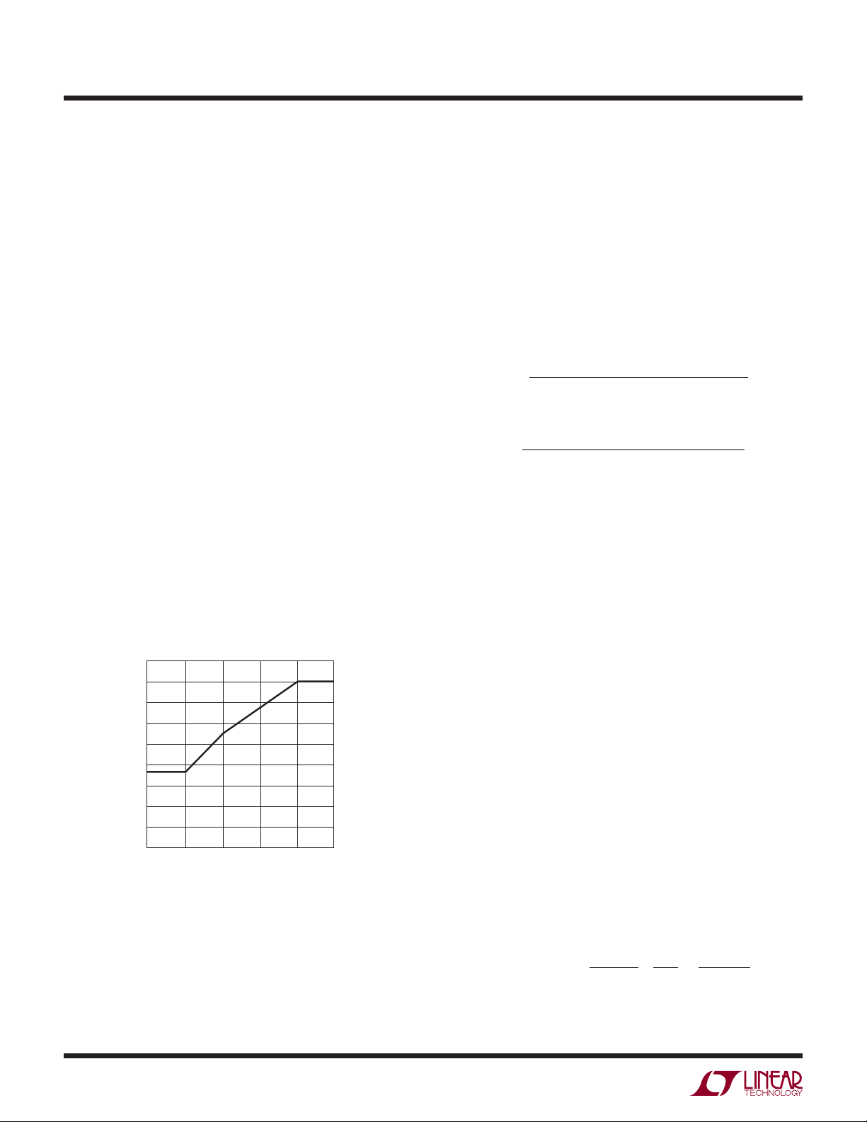
Selection of Operation Frequency
The LTC3780 uses a constant frequency architecture and
has an internal voltage controlled oscillator. The switching
frequency is determined by the internal oscillator capacitor.
This internal capacitor is charged by a fi xed current plus
an additional current that is proportional to the voltage
applied to the PLLFLTR pin. The frequency of this oscillator
can be varied over a 2-to-1 range. The PLLFLTR pin can
be grounded to lower the frequency to 200kHz or tied to
2.4V to yield approximately 400kHz. When PLLIN is left
open, the PLLFLTR pin goes low, forcing the oscillator to
minimum frequency.
A graph for the voltage applied to the PLLFLTR pin vs
frequency is given in Figure 7. As the operating frequency
is increased the gate charge losses will be higher, reducing
effi ciency. The maximum switching frequency is approximately 400kHz.
450
400
350
300
250
200
150
100
OPERATING FREQUENCY (kHz)
50
0
0
0.5 1.5
1
PLLFLTR PIN VOLTAGE (V)
Figure 7. Frequency vs PLLFLTR Pin Voltage
2.5
2
3780 F07
Inductor Selection
The operating frequency and inductor selection are interrelated in that higher operating frequencies allow the use
of smaller inductor and capacitor values. The inductor
value has a direct effect on ripple current. The inductor
current ripple ΔI
maximum inductor current at boost mode V
is typically set to 20% to 40% of the
L
. For
IN(MIN)
a given ripple the inductance terms in continuous mode
are as follows:
2
•– •
IN MIN OUT IN MIN
() ()
•
ƒ
OUT IN MAX O
I Ripple V
OUT MAX IN MAX
()
I
MMAX OUT
OUT
(
•–
()
() ()
Ripple V
•% •
)
()
UUT
•
100
100
2
H
,
H
L
BOOST
L
BUCK
VVV
>
VV V
>
••%•
ƒ
where:
f is operating frequency, Hz
% Ripple is allowable inductor current ripple, %
V
V
V
I
OUT(MAX)
is minimum input voltage, V
IN(MIN)
IN(MAX)
OUT
is maximum input voltage, V
is output voltage, V
is maximum output load current
For high effi ciency, choose an inductor with low core loss,
such as ferrite and molypermalloy (from Magnetics, Inc.).
Also, the inductor should have low DC resistance to reduce
2
R losses, and must be able to handle the peak inductor
the I
current without saturating. To minimize radiated noise,
use a toroid, pot core or shielded bobbin inductor.
R
R
Selection and Maximum Output Current
SENSE
is chosen based on the required output current.
SENSE
The current comparator threshold sets the peak of the
inductor current in boost mode and the maximum inductor
valley current in buck mode. In boost mode, the maximum
average load current at V
IN(MIN)
is:
16
I
OUT MAX BOOST
(, )
⎛
⎜
⎝
160
R
SENSE
mV
Δ
L
–•=
⎟
2
⎠
IN
V
MMIN
(
OUT
)
3780fe
V
⎞
I
Page 17
APPLICATIONS INFORMATION
LTC3780
where ΔIL is peak-to-peak inductor ripple current. In buck
mode, the maximum average load current is:
I
OUT MAX BUCK
(, )
130
=+
R
SENSE
Figure 8 shows how the load current (I
L
2
MAXLOAD
• R
SENSE
)
I
Δ
mV
varies with input and output voltage
The maximum current sensing R
value for the boost
SENSE
mode is:
R
SENSE MAX
•
2
I
OUT MAX BOOS
The maximum current sensing R
=
()
2 160
(,
••
mV V
IN MIN
()
VI V
••+Δ
TT OUT L BOOST IN MIN
),()
value for the buck
SENSE
mode is:
R
SENSE MAX
The fi nal R
R
SENSE(MAX)
=
()
SENSE
•–
2 Δ
value should be lower than the calculated
2 130
II
OUT MAX BUCK L BUC
(, ) ,
in both the boost and buck modes. A 20% to
mV
KK
•
30% margin is usually recommended.
input square wave current. Use a low ESR capacitor sized
to handle the maximum RMS current. For buck operation,
the input RMS current is given by:
V
II
≈
RMS OUT MAX
()
OUT
•• –1
V
IN
This formula has a maximum at VIN = 2V
I
RMS
= I
OUT(MAX)
/2. This simple worst-case condition
V
V
IN
OUT
OUT
, where
is commonly used for design because even signifi cant
deviations do not offer much relief. Note that ripple current ratings from capacitor manufacturers are often based
on only 2000 hours of life which makes it advisable to
derate the capacitor.
In boost mode, the discontinuous current shifts from the
input to the output, so C
must be capable of reducing
OUT
the output voltage ripple. The effects of ESR (equivalent
series resistance) and the bulk capacitance must be
considered when choosing the right capacitor for a given
output ripple voltage. The steady ripple due to charging
and discharging the bulk capacitance is given by:
Ripple Boost Cap
(,)
IVV
OUT MAX OUT IN MIN
=
•–
() ()
()
CVf
••
OUT OUT
V
C
IN
and C
Selection
OUT
In boost mode, input current is continuous. In buck mode,
input current is discontinuous. In buck mode, the selection
of input capacitor C
160
150
(mV)
140
SENSE
130
• R
120
MAX(LOAD)
I
110
100
0.1
Figure 8. Load Current vs VIN/V
is driven by the need to fi lter the
IN
110
VIN/V
(V)
OUT
3780 F08
OUT
Ripple Buck Cap
(,)
where C
is the output fi lter capacitor.
OUT
IVV
OUT MAX IN MAX OUT
=
•–
() ()
()
CV f
••
OUT IN MAX
()
V
The steady ripple due to the voltage drop across the ESR
is given by:
ΔV
ΔV
BOOST,ESR
BUCK,ESR
= I
L(MAX,BOOST)
= I
L(MAX,BUCK)
• ESR
• ESR
Multiple capacitors placed in parallel may be needed to
meet the ESR and RMS current handling requirements.
Dry tantalum, special polymer, aluminum electrolytic and
ceramic capacitors are all available in surface mount
packages. Ceramic capacitors have excellent low ESR
characteristics but can have a high voltage coeffi cient.
Capacitors are now available with low ESR and high ripple
current ratings, such as OS-CON and POSCAP.
3780fe
17
Page 18
LTC3780
APPLICATIONS INFORMATION
Power MOSFET Selection and
Effi ciency Considerations
The LTC3780 requires four external N-channel power
MOSFETs, two for the top switches (switch A and D, shown
in Figure 1) and two for the bottom switches (switch B and C
shown in Figure 1). Important parameters for the power
MOSFETs are the breakdown voltage V
voltage V
GS,TH
capacitance C
, on-resistance R
and maximum current I
RSS
, reverse transfer
DS(ON)
BR,DSS
DS(MAX)
, threshold
.
The drive voltage is set by the 6V INTVCC supply. Consequently, logic-level threshold MOSFETs must be used
in LTC3780 applications. If the input voltage is expected
to drop below 5V, then the sub-logic threshold MOSFETs
should be considered.
In order to select the power MOSFETs, the power dissipated by the device must be known. For switch A, the
maximum power dissipation happens in boost mode, when
it remains on all the time. Its maximum power dissipation
at maximum output current is given by:
2
⎞
ρ
⎟
⎠
P
A BOOST
⎛
V
OUT
IR
⎜
⎝
•••=
OUT MAX T DS ON,()()
V
IN
Switch B operates in buck mode as the synchronous
rectifi er. Its power dissipation at maximum output current
is given by:
–
P
BBUCK
VV
IN OUT
V
IN
•••=
IR
OUT MAX T DS ON,()()
2
ρ
Switch C operates in boost mode as the control switch. Its
power dissipation at maximum current is given by:
–
VVV
()
OUT IN OUT
P
CBOOST
,()()
where C
=
+
kV
is usually specifi ed by the MOSFET manufactur-
RSS
2
V
IN
3
•• ••
OUT
•••
IR
OUT MAX T DS ON
I
OUT MAX
()
V
IN
2
ρ
Cf
RSS
ers. The constant k, which accounts for the loss caused
by reverse recovery current, is inversely proportional to
the gate drive current and has an empirical value of 1.7.
For switch D, the maximum power dissipation happens in
boost mode, when its duty cycle is higher than 50%. Its
maximum power dissipation at maximum output current
is given by:
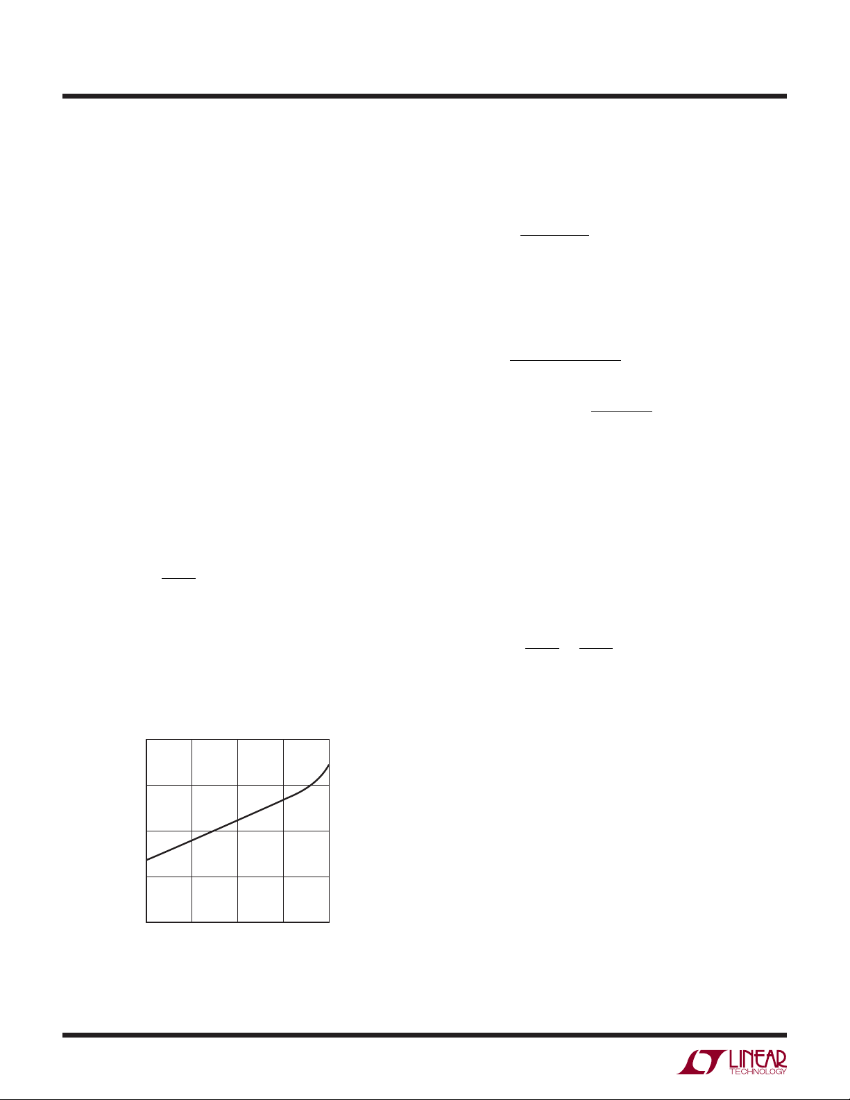
where ρT is a normalization factor (unity at 25°C) accounting for the signifi cant variation in on-resistance with
temperature, typically about 0.4%/°C as shown in Figure 9.
For a maximum junction temperature of 125°C, using a
value ρ
= 1.5 is reasonable.
T
2.0
1.5
1.0
0.5
NORMALIZED ON-RESISTANCE (Ω)
T
R
0
–50
Figure 9. Normalized R
0
JUNCTION TEMPERATURE (°C)
50
DS(ON)
100
vs Temperature
150
3780 F09
2
⎞
ρ
TTDSON
⎟
⎠
R•
()
P
D BOOST
V
V
IN
OUT
⎛
V
OUT
•• •=
⎜
⎝
I
OUT MAX,()
V
IN
For the same output voltage and current, switch A has the
highest power dissipation and switch B has the lowest
power dissipation unless a short occurs at the output.
From a known power dissipated in the power MOSFET, its
junction temperature can be obtained using the following
formula:
= TA + P • R
T
J
The R
TH(JA)
the R
TH(JC)
the case to the ambient temperature (R
can then be compared to the original, assumed value
of T
J
TH(JA)
to be used in the equation normally includes
for the device plus the thermal resistance from
). This value
TH(JC)
used in the iterative calculation process.
3780fe
18
Page 19

APPLICATIONS INFORMATION
LTC3780
Schottky Diode (D1, D2) Selection
and Light Load Operation
The Schottky diodes D1 and D2 shown in Figure 1 conduct
during the dead time between the conduction of the power
MOSFET switches. They are intended to prevent the body
diode of synchronous switches B and D from turning on
and storing charge during the dead time. In particular, D2
signifi cantly reduces reverse recovery current between
switch D turn-off and switch C turn-on, which improves
converter effi ciency and reduces switch C voltage stress.
In order for the diode to be effective, the inductance
between it and the synchronous switch must be as small
as possible, mandating that these components be placed
adjacently.
In buck mode, when the FCB pin voltage is 0.85 < V
FCB
< 5V, the converter operates in skip-cycle mode. In this
mode, synchronous switch B remains off until the inductor peak current exceeds one-fi fth of its maximum peak
current. As a result, D1 should be rated for about one-half
to one-third of the full load current.
In boost mode, when the FCB pin voltage is higher than
5.3V, the converter operates in discontinuous current mode.
In this mode, synchronous switch D remains off until the
inductor peak current exceeds one-fi fth of its maximum
peak current. As a result, D2 should be rated for about
one-third to one-fourth of the full load current.
In buck mode, when the FCB pin voltage is higher than 5.3V,
the converter operates in constant frequency discontinuous current mode. In this mode, synchronous switch B
remains on until the inductor valley current is lower than
the sense voltage representing the minimum negative
inductor current level (V
= –5mV). Both switch A
SENSE
and B are off until next clock signal.
In boost mode, when the FCB pin voltage is 0.85 < V
FCB
< 5.3V, the converter operates in Burst Mode operation.
In this mode, the controller clamps the peak inductor
current to approximately 20% of the maximum inductor
current. The output voltage ripple can increase during
Burst Mode operation.
INTV
Regulator
CC
An internal P-channel low dropout regulator produces 6V
at the INTV
pin from the VIN supply pin. INTVCC powers
CC
the drivers and internal circuitry within the LTC3780. The
INTV
pin regulator can supply a peak current of 40mA
CC
and must be bypassed to ground with a minimum of 4.7μF
tantalum, 10μF special polymer or low ESR type electrolytic
capacitor. A 1μF ceramic capacitor placed directly adjacent
to the INTV
and PGND IC pins is highly recommended.
CC
Good bypassing is necessary to supply the high transient
current required by MOSFET gate drivers.
Higher input voltage applications in which large MOSFETs
are being driven at high frequencies may cause the maximum junction temperature rating for the LTC3780 to be
exceeded. The system supply current is normally dominated
by the gate charge current. Additional external loading of
the INTV
power dissipation calculations. The total INTV
also needs to be taken into account for the
CC
current
CC
can be supplied by either the 6V internal linear regulator
or by the EXTV
the EXTV
CC
input pin. When the voltage applied to
CC
pin is less than 5.7V, all of the INTVCC current
is supplied by the internal 6V linear regulator. Power dissipation for the IC in this case is V
IN
• I
INTVCC
, and overall
effi ciency is lowered. The junction temperature can be
estimated by using the equations given in Note 2 of the
Electrical Characteristics. For example, a typical application
operating in continuous current mode might draw 24mA
from a 24V supply when not using the EXTV
= 70°C + 24mA • 24V • 34°C/W = 90°C
T
J
Use of the EXTV
input pin reduces the junction tem-
CC
CC
pin:
perature to:
= 70°C + 24mA • 6V • 34°C/W = 75°C
T
J
To prevent maximum junction temperature from being
exceeded, the input supply current must be checked
operating in continuous mode at maximum V
IN
.
3780fe
19
Page 20

LTC3780
APPLICATIONS INFORMATION
EXTVCC Connection
The LTC3780 contains an internal P-channel MOSFET
switch connected between the EXTV
When the voltage applied to EXTV
and INTVCC pins.
CC
rises above 5.7V, the
CC
internal regulator is turned off and a switch connects the
EXTV
pin to the INTVCC pin thereby supplying internal
CC
power. The switch remains closed as long as the voltage
applied to EXTV
remains above 5.5V. This allows the
CC
MOSFET driver and control power to be derived from the
output when (5.7V < V
< 7V) and from the internal
OUT
regulator when the output is out of regulation (start-up,
short-circuit). If more current is required through the
EXTV
diode can be interposed between the EXTV
pins. Ensure that EXTV
switch than is specifi ed, an external Schottky
CC
and INTVCC
CC
≤ VIN.
CC
The following list summarizes the three possible connections for EXTV
1. EXTV
CC
:
CC
left open (or grounded). This will cause INTVCC
to be powered from the internal 6V regulator at the cost
of a small effi ciency penalty.
2. EXTV
connected directly to V
CC
(5.7V < V
OUT
OUT
< 7V).
This is the normal connection for a 6V regulator and
provides the highest effi ciency.
3. EXTV
connected to an external supply. If an external
CC
supply is available in the 5.5V to 7V range, it may be
used to power EXTV
provided it is compatible with
CC
the MOSFET gate drive requirements.
Output Voltage
The LTC3780 output voltage is set by an external feedback
resistive divider carefully placed across the output capacitor.
The resultant feedback signal is compared with the internal
precision 0.800V voltage reference by the error amplifi er.
The output voltage is given by the equation:
VV
=+
08 1
OUT
.•
⎛
⎜
⎝
⎞
⎟
⎠
R
1
R
2
Topside MOSFET Driver Supply (CA, DA, CB, DB)
Referring to Figure 11, the external bootstrap capacitors
and CB connected to the BOOST1 and BOOST2 pins
C
A
supply the gate drive voltage for the topside MOSFET
switches A and D. When the top MOSFET switch A turns
on, the switch node SW2 rises to V
pin rises to approximately V
+ INTVCC. When the bottom
IN
and the BOOST2
IN
MOSFET switch B turns on, the switch node SW2 drops
to low and the boost capacitor C
from INTV
. When the top MOSFET switch D turns on,
CC
the switch node SW1 rises to V
rises to approximately V
OUT
is charged through DB
B
and the BOOST1 pin
OUT
+ INTVCC. When the bottom
MOSFET switch C turns on, the switch node SW1 drops
to low and the boost capacitor C
from INTV
. The boost capacitors CA and CB need to
CC
is charged through DA
A
store about 100 times the gate charge required by the top
MOSFET switch A and D. In most applications a 0.1μF to
0.47μF, X5R or X7R dielectric capacitor is adequate.
Run Function
The RUN pin provides simple ON/OFF control for the
LTC3780. Driving the RUN pin above 1.5V permits the
controller to start operating. Pulling RUN below 1.5V puts
the LTC3780 into low current shutdown. Do not apply more
than 6V to the RUN pin.
Soft-Start Function
Soft-start reduces the input power sources’ surge currents by gradually increasing the controller’s current
limit (proportional to an internally buffered and clamped
equivalent of V
An internal 1.2μA current source charges up the C
ITH
).
SS
capacitor. As the voltage on SS increases from 0V to
2.4V, the internal current limit rises from 0V/R
150mV/R
. The output current limit ramps up slowly,
SENSE
SENSE
to
taking 1.5s/μF to reach full current. The output current thus
ramps up slowly, eliminating the starting surge current
required from the input power supply.
24
.
V
T
=
IRMP SS SS
12
•./•
.
CsFC
A
μ
15
=μ
()
Do not apply more than 6V to the SS pin.
Current foldback is disabled during soft-start until the
voltage on C
reaches 2V. Make sure CSS is large enough
SS
when there is loading during start-up.
20
3780fe
Page 21

APPLICATIONS INFORMATION
LTC3780
The Standby Mode (STBYMD) Pin Function
The standby mode (STBYMD) pin provides several choices
for start-up and standby operational modes. If the pin is
pulled to ground, the SS pin is internally pulled to ground,
preventing start-up and thereby providing a single control
pin for turning off the controller. If the pin is left open or
bypassed to ground with a capacitor, the SS pin is internally
provided with a starting current, permitting external control
for turning on the controller. If the pin is connected to a
voltage greater than 1.25V, the internal regulator (INTV
CC
)
will be on even when the controller is shut down (RUN
pin voltage < 1.5V). In this mode, the onboard 6V linear
regulator can provide power to keep-alive functions such
as a keyboard controller.
Fault Conditions: Current Limit and Current Foldback
The maximum inductor current is inherently limited in a
current mode controller by the maximum sense voltage.
In boost mode, maximum sense voltage and the sense
resistance determines the maximum allowed inductor
peak current, which is:
mV
I
L MAX BOOST
(, )
=
160
R
SENSE
In buck mode, maximum sense voltage and the sense
resistance determines the maximum allowed inductor
valley current, which is:
Fault Conditions: Overvoltage Protection
A comparator monitors the output for overvoltage conditions. The comparator (OV) detects overvoltage faults
greater than 7.5% above the nominal output voltage.
When the condition is sensed, switches A and C are
turned off, and switches B and D are turned on until the
overvoltage condition is cleared. During an overvoltage
condition, a negative current limit (V
= –60mV) is
SENSE
set to limit negative inductor current. When the sensed
current inductor current is lower than –60mV, switch A and
C are turned on, and switch B and D are turned off until
the sensed current is higher than –20mV. If the output is
still in overvoltage condition, switch A and C are turned
off, and switch B and D are turned on again.
Effi ciency Considerations
The percent effi ciency of a switching regulator is equal to
the output power divided by the input power times 100%.
It is often useful to analyze individual losses to determine
what is limiting the effi ciency and which change would
produce the most improvement. Although all dissipative
elements in circuit produce losses, four main sources
account for most of the losses in LTC3780 circuits:
2
1. DC I
R losses. These arise from the resistances of the
MOSFETs, sensing resistor, inductor and PC board
traces and cause the effi ciency to drop at high output
currents.
mV
I
L MAX BUCK
(, )
=
130
R
SENSE
To further limit current in the event of a short circuit to
ground, the LTC3780 includes foldback current limiting.
If the output falls by more than 30%, then the maximum
sense voltage is progressively lowered to about one third
of its full value.
2. Transition loss. This loss arises from the brief amount
of time switch A or switch C spends in the saturated
region during switch node transitions. It depends upon
the input voltage, load current, driver strength and
MOSFET capacitance, among other factors. The loss
is signifi cant at input voltages above 20V and can be
estimated from:
Transition Loss ≈ 1.7A
where C
is the reverse transfer capacitance.
RSS
IN2
OUT
• C
RSS
• f
3780fe
–1
• V
• I
21
Page 22

LTC3780
APPLICATIONS INFORMATION
3. INTVCC current. This is the sum of the MOSFET driver
and control currents. This loss can be reduced by supplying INTV
current through the EXTVCC pin from a
CC
high effi ciency source, such as an output derived boost
network or alternate supply if available.
4. C
and C
IN
loss. The input capacitor has the diffi cult
OUT
job of fi ltering the large RMS input current to the regulator in buck mode. The output capacitor has the more
diffi cult job of fi ltering the large RMS output current
in boost mode. Both C
and C
IN
low ESR to minimize the AC I
are required to have
OUT
2
R loss and suffi cient
capacitance to prevent the RMS current from causing
additional upstream losses in fuses or batteries.
5. Other losses. Schottky diode D1 and D2 are responsible for conduction losses during dead time and light
load conduction periods. Inductor core loss occurs
predominately at light loads. Switch C causes reverse
recovery current loss in boost mode.
When making adjustments to improve effi ciency, the input
current is the best indicator of changes in effi ciency. If you
make a change and the input current decreases, then the
effi ciency has increased. If there is no change in input
current, then there is no change in effi ciency.
The highest value of ripple current occurs at the maximum
input voltage. In boost mode, the ripple current is:
⎛
V
Δ=
I
L BOOST
,
I
RIPPLE BOOST
,
IN IN
•–1
⎜
⎝
fL
•
Δ 100
I
L BOOST
,
I
The highest value of ripple current occurs at VIN = V
⎞
V
⎟
⎠
V
OUT
•
%=
IN
/2.
OUT
A 6.8μH inductor will produce 11% ripple in boost mode
= 6V) and 29% ripple in buck mode (VIN = 18V).
(V
IN
The R
resistor value can be calculated by using the
SENSE
maximum current sense voltage specifi cation with some
accommodation for tolerances.
R
SENSE
=
2
Select an R
••
IV
••
(, )
OUT MAX BOOST O
of 10mΩ.
SENSE
()
IN MIN
IV+Δ
UUT L BOOST IN MIN
,()
•
mV V
2 160
Output voltage is 12V. Select R1 as 20k. R2 is:
VR
R
OUT
2
08
.
1
•
R
1=
–
Design Example
As a design example, assume V
= 12V (5%), I
V
OUT
OUT(MAX)
= 5V to 18V (12V nominal),
IN
= 5A and f = 400kHz.
Set the PLLFLTR pin at 2.4V for 400kHz operation. The
inductance value is chosen fi rst based on a 30% ripple
current assumption. In buck mode, the ripple current is:
Δ=
I
LBUCK
,
I
RIPPLE BUCK
,
V
⎛
OUT OUT
•–1
⎜
fL
•
⎝
Δ 100
I
LBUCK
,
I
OUT
⎞
V
⎟
V
⎠
IN
•
%=
Select R2 as 280k. Both R1 and R2 should have a tolerance of no more than 1%.
Next, choose the MOSFET switches. A suitable choice is
the Siliconix Si4840 (R
= 150pF, θJA = 40°C/W).
C
RSS
= 0.009Ω (at VGS = 6V),
DS(ON)
The maximum power dissipation of switch A occurs in
boost mode when switch A stays on all the time. Assuming a junction temperature of T
1.5, the power dissipation at V
12
PW
A BOOST,
⎛
⎜
⎝
2
⎞
••.•. .=
5 1 5 0 009 1 94
⎟
⎠
5
= 150°C with ρ
J
= 5V is:
IN
=
150°C
3780fe
=
22
Page 23
APPLICATIONS INFORMATION
LTC3780
Double-check the TJ in the MOSFET with 70°C ambient
temperature:
= 70°C + 1.94W • 40°C/W = 147.6°C
T
J
The maximum power dissipation of switch B occurs in buck
mode. Assuming a junction temperature of T
= 1.2, the power dissipation at VIN = 18V is:
ρ
80°C
–
PmW
BBUCK,
18 12
18
2
••.•.==
5 1 2 0 009 90
= 80°C with
J
Double-check the TJ in the MOSFET at 70°C ambient
temperature:
= 70°C + 0.09W • 40°C/W = 73.6°C
T
J
The maximum power dissipation of switch C occurs in boost
mode. Assuming a junction temperature of T
= 1.4, the power dissipation at VIN = 5V is:
ρ
110°C
12 5 12
–•
()
P
C BOOST,
=
+
212
•••
2
5
3
2
5 1 4 0 009
••.•.
5
1150 400 1 27pk W•.=
5
= 110°C with
J
Double-check the TJ in the MOSFET at 70°C ambient
temperature:
C
is chosen to fi lter the square current in buck mode. In
IN
this mode, the maximum input current peak is:
IA
IN PEAK MAX BUCK,(, )
⎛
•
⎜
⎝
A low ESR (10mΩ) capacitor is selected. Input voltage
ripple is 57mV (assuming ESR dominate ripple).
is chosen to fi lter the square current in boost mode.
C
OUT
In this mode, the maximum output current peak is:
I
OUT PEAK MAX BOOST,(, )
12
5
••
A low ESR (5mΩ) capacitor is suggested. This capacitor
will limit output voltage ripple to 53mV (assuming ESR
dominate ripple).
PC Board Layout Checklist
The basic PC board layout requires a dedicated ground
plane layer. Also, for high current, a multilayer board
provides heat sinking for power components.
• The ground plane layer should not have any traces and
it should be as close as possible to the layer with power
MOSFETs.
= 70°C + 1.08W • 40°C/W = 113°C
T
J
The maximum power dissipation of switch D occurs
in boost mode when its duty cycle is higher than 50%.
Assuming a junction temperature of T
= 1.35, the power dissipation at VIN = 5V is:
ρ
100°C
51212
PW
D BOOST,
⎛
•••.•. .=
⎜
⎝
5
2
⎞
5 1 35 0 009 0 73
⎟
⎠
= 100°C with
J
=
Place CIN, switch A, switch B and D1 in one com-
•
pact area. Place C
, switch C, switch D and D2 in
OUT
one compact area. One layout example is shown in
Figure 10.
V
IN
QA
SW2 SW1
L
%
29
⎞
=51
⎟
⎠
2
⎛
51
⎜
⎝
11
.=+
57
%
2
D2
QD
⎞
⎟
⎠
=
10 66A
V
.=+
OUT
Double-check the TJ in the MOSFET at 70°C ambient
temperature:
= 70°C + 0.73W • 40°C/W = 99°C
T
J
D1
QCQB
C
IN
R
SENSE
LTC3780
CKT
Figure 10. Switches Layout
C
OUT
GND
3780 F10
3780fe
23
Page 24

LTC3780
APPLICATIONS INFORMATION
• Use immediate vias to connect the components (including the LTC3780’s SGND and PGND pins) to the
ground plane. Use several large vias for each power
component.
• Use planes for V
and V
IN
to maintain good voltage
OUT
fi ltering and to keep power losses low.
• Flood all unused areas on all layers with copper. Flooding
with copper will reduce the temperature rise of power
components. Connect the copper areas to any DC net
or GND).
(V
IN
• Segregate the signal and power grounds. All smallsignal components should return to the SGND pin at
one point, which is then tied to the PGND pin close to
the sources of switch B and switch C.
• Place switch B and switch C as close to the controller
as possible, keeping the PGND, BG and SW traces
short.
• Keep the high dV/dT SW1, SW2, BOOST1, BOOST2,
TG1 and TG2 nodes away from sensitive small-signal
nodes.
• The path formed by switch A, switch B, D1 and the C
IN
capacitor should have short leads and PC trace lengths.
The path formed by switch C, switch D, D2 and the
capacitor also should have short leads and PC
C
OUT
trace lengths.
• The output capacitor (–) terminals should be connected
as close as possible the (–) terminals of the input
capacitor.
• Connect the top driver boost capacitor C
closely to the
A
BOOST1 and SW1 pins. Connect the top driver boost
capacitor C
• Connect the input capacitors C
closely to the power MOSFETs. These capaci-
C
OUT
closely to the BOOST2 and SW2 pins.
B
and output capacitors
IN
tors carry the MOSFET AC current in boost and buck
mode.
• Connect V
nals of C
OUT
OSENSE
pin resistive dividers to the (+) termi-
and signal ground. A small V
OSENSE
bypass
capacitor may be connected closely to the LTC3780 SGND
pin. The R2 connection should not be along the high
current or noise paths, such as the input capacitors.
–
• Route SENSE
and SENSE+ leads together with minimum
PC trace spacing. Avoid sense lines pass through noisy
area, such as switch nodes. The fi lter capacitor between
+
SENSE
and SENSE– should be as close as possible
to the IC. Ensure accurate current sensing with Kelvin
connections at the SENSE resistor. One layout example
is shown in Figure 12.
• Connect the I
IC, between I
pin compensation network close to the
TH
and the signal ground pins. The capaci-
TH
tor helps to fi lter the effects of PCB noise and output
voltage ripple voltage from the compensation loop.
• Connect the INTV
IC, between the INTV
bypass capacitor, C
CC
and the power ground pins. This
CC
, close to the
VCC
capacitor carries the MOSFET drivers’ current peaks.
An additional 1μF ceramic capacitor placed immediately
next to the INTV
and PGND pins can help improve
CC
noise performance substantially.
24
3780fe
Page 25
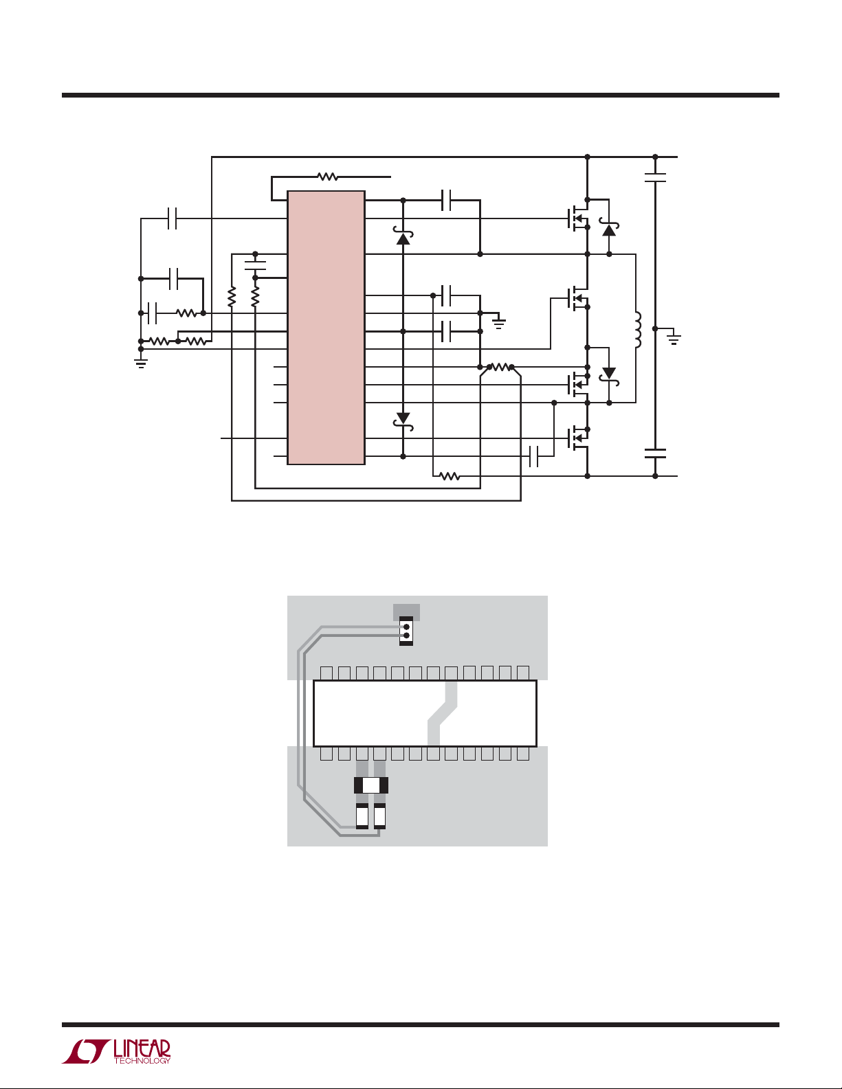
APPLICATIONS INFORMATION
R
PU
C
SS
C
C2
C
C1
R
C
R2
R1
RR
f
IN
C
1
2
3
4
5
6
7
8
9
10
11
12
PGOOD
SS
LTC3780
SENSE
SENSE
I
TH
V
OSENSE
SGND
RUN
FCB
PLLFLTR
PLLIN
STBYMD
+
–
BOOST1
TG1
SW1
V
EXTV
INTV
BG1
PGND
BG2
SW2
TG2
BOOST2
IN
CC
CC
LTC3780
V
OUT
V
PULLUP
24
23
22
21
20
19
18
17
16
15
14
13
C
A
D
D
A
C
F
C
VCC
R
SENSE
D
B
C
B
R
IN
D2
C
D1
B
A
C
OUT
L
C
IN
V
IN
3780 F11
Figure 11. LTC3780 Layout Diagram
SENSE
R
2423222120191817161514
1
2
3
4
5
6
7
8
9
101112
C
RR
Figure 12. Sense Lines Layout
PGND
13
SGND
3780 F12
3780fe
25
Page 26
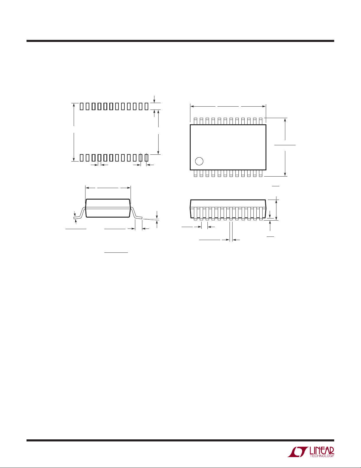
LTC3780
PACKAGE DESCRIPTION
G Package
24-Lead Plastic SSOP (5.3mm)
(Reference LTC DWG # 05-08-1640)
1.25 p0.12
7.8 – 8.2
0.42 p0.03
RECOMMENDED SOLDER PAD LAYOUT
5.00 – 5.60**
(.197 – .221)
0.09 – 0.25
(.0035 – .010)
NOTE:
1. CONTROLLING DIMENSION: MILLIMETERS
2. DIMENSIONS ARE IN
3. DRAWING NOT TO SCALE
*
DIMENSIONS DO NOT INCLUDE MOLD FLASH. MOLD FLASH
SHALL NOT EXCEED .152mm (.006") PER SIDE
**
DIMENSIONS DO NOT INCLUDE INTERLEAD FLASH. INTERLEAD
FLASH SHALL NOT EXCEED .254mm (.010") PER SIDE
0.55 – 0.95
(.022 – .037)
MILLIMETERS
(INCHES)
5.3 – 5.7
0.65 BSC
0o – 8o
7.90 – 8.50*
(.311 – .335)
2122 18 17 16 15 14
19202324
12345678 9 10 11 12
0.65
(.0256)
BSC
0.22 – 0.38
(.009 – .015)
TYP
13
(.291 – .323)
2.0
(.079)
MAX
0.05
(.002)
MIN
G24 SSOP 0204
7.40 – 8.20
26
3780fe
Page 27
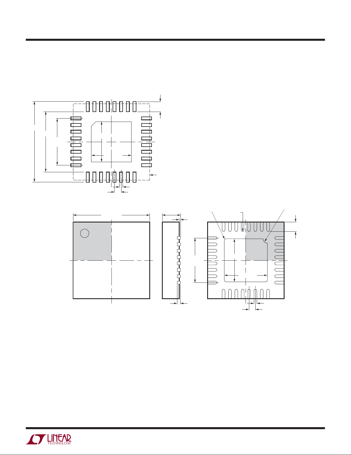
PACKAGE DESCRIPTION
5.50 p0.05
4.10 p0.05
(4 SIDES)
3.50 REF
APPLY SOLDER MASK TO AREAS THAT ARE NOT SOLDERED
3.45 p 0.05
3.45 p 0.05
RECOMMENDED SOLDER PAD LAYOUT
5.00 p 0.10
(4 SIDES)
PIN 1
TOP MARK
(NOTE 6)
UH Package
32-Lead Plastic QFN (5mm × 5mm)
(Reference LTC DWG # 05-08-1693 Rev D)
0.70 p0.05
PACKAGE OUTLINE
0.25 p 0.05
0.50 BSC
0.75 p 0.05
R = 0.05
0.00 – 0.05
TYP
BOTTOM VIEW—EXPOSED PAD
R = 0.115
TYP
31
LTC3780
PIN 1 NOTCH R = 0.30 TYP
OR 0.35 s 45o CHAMFER
32
1
2
0.40 p 0.10
3.50 REF
(4-SIDES)
0.200 REF
NOTE:
1. DRAWING PROPOSED TO BE A JEDEC PACKAGE OUTLINE
M0-220 VARIATION WHHD-(X) (TO BE APPROVED)
2. DRAWING NOT TO SCALE
3. ALL DIMENSIONS ARE IN MILLIMETERS
4. DIMENSIONS OF EXPOSED PAD ON BOTTOM OF PACKAGE DO NOT INCLUDE
MOLD FLASH. MOLD FLASH, IF PRESENT, SHALL NOT EXCEED 0.20mm ON ANY SIDE
5. EXPOSED PAD SHALL BE SOLDER PLATED
6. SHADED AREA IS ONLY A REFERENCE FOR PIN 1 LOCATION
ON THE TOP AND BOTTOM OF PACKAGE
3.45 p 0.10
3.45 p 0.10
(UH32) QFN 0406 REV D
0.25 p 0.05
0.50 BSC
Information furnished by Linear Technology Corporation is believed to be accurate and reliable.
However, no responsibility is assumed for its use. Linear Technology Corporation makes no representation that the interconnection of its circuits as described herein will not infringe on existing patent rights.
3780fe
27
Page 28
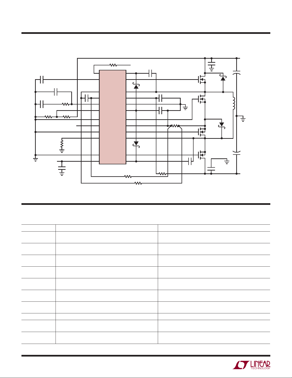
LTC3780
TYPICAL APPLICATION
C
SS
0.022μF
C
C2
C
C1
0.01μF
8.06k, 1%
R1
47pF
2V
R
C
100k
R2 113k, 1%
ON/OFF
10k
C
STBYMD
0.01μF
68pF
1
2
3
4
5
6
7
8
9
10
11
12
PGOOD
SS
LTC3780
SENSE
SENSE
I
TH
V
OSENSE
SGND
RUN
FCB
PLLFLTR
PLLIN
STBYMD
R
+
–
PU
BOOST1
TG1
SW1
EXTV
INTV
BG1
PGND
BG2
SW2
TG2
BOOST2
V
IN
CC
CC
24
23
22
21
20
19
18
17
16
15
14
13
100Ω
V
PULLUP
100Ω
0.22μF
D
A
BO540W
D
B
BO540W
V
OUT
12V
L
3780 TA02
+
+
5A
C
OUT
330μF
16V
C
IN
22μF
35V
V
IN
5V TO 32V
D
Si7884DP
C
Si7884DP
B
Si7884DP
A
Si7884DP
22μF
16V, X7R
s 3
D2
B320A
4.7μH
D1
B340A
3.3μF
50V, X5R
s 3
C
A
C
0.1μF
F
4.7μF
C
VCC
9mΩ
10Ω
CB0.22μF
Figure 13. LTC3780 12V/5A, Buck-Boost Regulator
RELATED PARTS
PART NUMBER DESCRIPTION COMMENTS
LTC1871/LTC1871-1
LTC1871-7
LTC3443 1.2A I
LTC3444 500mA I
LTC3531/LTC3531-3
LTC3531-3.3
LTC3532 500mA I
LTC3533 2A Wide Input Voltage Synchronous Buck-Boost DC/DC
LTC3785/LTC3785-1 10V, High Effi ciency, Synchronous, No R
SEPIC, Boost, Flyback Controller No R
Package
OUT
Converter
Converter
200mA I
, 600kHz, Synchronous Buck-Boost DC/DC
, 1.5MHz Synchronous Buck-Boost DC/DC
OUT
, Synchronous Buck-Boost DC/DC Converter VIN: 1.8V to 5.5V, V
OUT
VIN: 2.4V to 5.5V, V
MS Package
VIN: 2.7V to 5.5V, V
Amplifi er Bias
MS, DFN Packages
Converter
, 2MHz, Synchronous Buck-Boost DC/DC
OUT
VIN: 2.4V to 5.5V, V
MS, DFN Packages
VIN: 1.8V to 5.5V, V
Converter
Controller
, Buck-Boost
SENSE
DFN Package
VIN: 2.7V to 10V, V
QFN-24 Package
LTC4444/LTC4444-5 High Voltage Synchronous N-Channel MOSFET Driver VIN up to 100V, Used with the LTC3780 for Higher VIN Applications
LTM4605 5A to 12A Buck-Boost μModule™
4.5V ≤ VIN ≤ 20V, 0.8V ≤ V
LGA Package
LTM4607 5A to 12A Buck-Boost μModule
4.5V ≤ V
LGA Package
No R
and μModule are trademarks of Linear Technology Corporation
SENSE
Linear Technology Corporation
28
1630 McCarthy Blvd., Milpitas, CA 95035-7417
(408) 432-1900 ● FAX: (408) 434-0507
●
www.linear.com
™, 2.5V ≤ VIN ≤ 36V Burst Mode Operation, MSOP-10
SENSE
: 2.4V to 5.25V, IQ = 28μA, ISD < 1μA,
OUT
: 0.5V to 5.25V, Optimized for WCDMA RF
OUT
: 2V to 5V, IQ = 35μA, ISD < 1μA,
OUT
: 2.4V to 5.25V, IQ = 35μA, ISD < 1μA,
OUT
: 1.8V to 5.25V, IQ = 40μA, ISD < 1μA,
OUT
: 2.7V to 10V, IQ = 86mA, ISD < 15μA,
OUT
≤ 16V, 15mm × 15mm × 2.8mm
OUT
≤ 36V, 0.8V ≤ V
IN
≤ 24V, 15mm × 15mm × 2.8mm
OUT
LT 0309 REV E • PRINTED IN USA
© LINEAR TECHNOLOGY CORPORATION 2005
3780fe
 Loading...