


LT3505
1.2A, Step-Down
Switching Regulator in
3mm × 3mm DFN
FEATURES
!
Wide Input Range: 3.6V to 36V Operating,
40V Maximum
!
Up to 1.2A Output Current
!
Resistor-Programmable Fixed-Frequency Operation
from 200kHz to 3MHz
!
Output Adjustable Down to 780mV
!
Short-Circuit Robust
!
Uses Tiny Capacitors and Inductors
!
Soft-Start
!
Low Shutdown Current: <2µA
!
Low V
!
Thermally Enhanced, Low Profi le 3mm x 3mm
Switch: 350mV at 1A
CESAT
DFN-8 and MSOP-8 Packages
APPLICATIONS
!
Automotive Battery Regulation
!
Industrial Control Supplies
!
Wall Transformer Regulation
!
Distributed Supply Regulation
!
Battery-Powered Equipment
DESCRIPTION
The LT®3505 is a current mode PWM step-down DC/DC
converter with an internal 1.4A power switch. The wide
operating input range of 3.6V to 36V (40V maximum)
makes the LT3505 ideal for regulating power from a wide
variety of sources, including unregulated wall transformers, 24V industrial supplies and automotive batteries. The
oscillator can be programmed for high frequency operation
allowing the use of tiny, low cost external components or
it can be programmed for lower frequency operation to
maximize effi ciency.
Cycle-by-cycle current limit provides protection against
shorted outputs and soft-start eliminates input current
surge during start-up. The low current (<2µA) shutdown
mode provides output disconnect, enabling easy power
management in battery-powered systems.
, LT, LTC and LTM are registered trademarks of Linear Technology Corporation.
All other trademarks are the property of their respective owners.
TYPICAL APPLICATION
750kHz, 3.3V Step-Down Converter
V
4.2V TO 36V
ON OFF
IN
1µF
V
IN
SHDN
R
T
75.0k
LT3505
GND
BOOST
SW
FB
V
C
69.8k
68pF
0.1µF
10µH
36.5k
11.3k
22pF
V
3.3V
1.1A, V
1.2A, V
10µF
3505 TA01
OUT
IN
IN
> 5V
> 8V
90
85
80
75
70
65
EFFICIENCY (%)
60
VIN = 12V
= 3.3V
V
OUT
55
= 750kHz
f
SW
L = 10 H
50
0.20
Effi ciency
0.6
0.8
0.4
LOAD CURRENT (A)
1.0
1.2
3505fc
1

LT3505
2
3505fc
Input Voltage (VIN) ....................................................40V
BOOST Pin Voltage ..................................................50V
BOOST Pin Above SW Pin .........................................25V
SHDN Pin ..................................................................40V
FB Pin .........................................................................6V
V
C
Pin .........................................................................3V
R
T
Pin .........................................................................3V
ABSOLUTE MAXIMUM RATINGS
(Note 1)
TOP VIEW
9
DD PACKAGE
8-LEAD (3mm × 3mm) PLASTIC DFN
5
6
7
8
4
3
2
1BOOST
SW
V
IN
SHDN
V
C
FB
R
T
GND
T
JMAX
= 125°C, θJA = 43°C/W, θ
JC
= 5°C/W
EXPOSED PAD (PIN 9) IS GND, MUST BE SOLDERED TO PCB
1
2
3
4
BOOST 8
7
6
5
9
V
C
FB
R
T
GND
TOP VIEW
MS8E PACKAGE
8-LEAD PLASTIC MSOP
SW
V
IN
SHDN
T
JMAX
= 125°C, θJA = 40°C/W, θ
JC
= 5°C/W
EXPOSED PAD (PIN 9) IS GND, MUST BE SOLDERED TO PCB
PIN CONFIGURATION
Operating Temperature Range (Note 2)
LT3505E .............................................. –40°C to 85°C
LT3505I ............................................. –40°C to 125°C
Maximum Junction Temperature .......................... 125°C
Storage Temperature Range ................... –65°C to 150°C
ORDER INFORMATION
LEAD FREE FINISH TAPE AND REEL PART MARKING PACKAGE DESCRIPTION TEMPERATURE RANGE
LT3505EDD#PBF LT3505EDD#TRPBF LCHB 8-Lead (3mm x 3mm) Plastic DFN –40°C to 85°C
LT3505IDD#PBF LT3505IDD#TRPBF LCHC 8-Lead (3mm x 3mm) Plastic DFN –40°C to 125°C
LT3505EMS8E#PBF LT3505EMS8E#TRPBF LTCNX 8-Lead Plastic MSOP –40°C to 85°C
LT3505IMS8E#PBF LT3505IMS8E#TRPBF LTCNY 8-Lead Plastic MSOP –40°C to 125°C
LEAD BASED FINISH TAPE AND REEL PART MARKING PACKAGE DESCRIPTION TEMPERATURE RANGE
LT3505EDD LT3505EDD#TR LCHB 8-Lead (3mm x 3mm) Plastic DFN –40°C to 85°C
LT3505IDD LT3505IDD#TR LCHC 8-Lead (3mm x 3mm) Plastic DFN –40°C to 125°C
LT3505EMS8E LT3505EMS8E#TR LTCNX 8-Lead Plastic MSOP –40°C to 85°C
LT3505IMS8E LT3505IMS8E#TR LTCNY 8-Lead Plastic MSOP –40°C to 125°C
Consult LTC Marketing for parts specifi ed with wider operating temperature ranges.
For more information on lead free part marking, go to: http://www.linear.com/leadfree/
For more information on tape and reel specifi cations, go to: http://www.linear.com/tapeandreel/

LT3505
ELECTRICAL CHARACTERISTICS
The " denotes the specifi cations which apply over the full operating
temperature range, otherwise specifi cations are at T
= 25°C, VIN = 12V, V
A
PARAMETER CONDITIONS MIN TYP MAX UNITS
Operating Range 3.6 36 V
V
IN
Undervoltage Lockout 3.1 3.35 3.6 V
Feedback Voltage
FB Pin Bias Current V
= Measured V
FB
Quiescent Current Not Switching, R
Quiescent Current in Shutdown V
Reference Line Regulation V
Switching Frequency V
Maximum Duty Cycle R
Error Amp Transconductance V
Error Amp Voltage Gain V
Source Current VFB = 0V, VC = 1.5V 10 µA
V
C
Sink Current VFB = 1V, VC = 1.5V 14 µA
V
C
Switching Threshold Voltage I
V
C
Clamp Voltage VFB = 0V 1.7 V
V
C
Bias Voltage VFB = 0.6V
R
T
= 0V 0.01 2 µA
SHDN
= 5V to 36V 0.007 %/V
IN
= 0.7V, RT = 13.7k
FB
V
= 0.7V, RT = 75.0k
FB
V
= 0.7V, RT = 357k
FB
= 75.0k
T
= 0.78V 200 µA/V
FB
= 0.78V 400 V/V
FB
= 0mA 0.9 V
OUT
V
= 0V, RT = 75.0k
FB
(Note 4)
REF
= 75.0k 2.0 2.7 mA
T
Switch Current Limit (Note 3) 1.4 1.75 2.2 A
Switch V
CESAT
ISW = 1A 350 mV
Switch Leakage Current 0.1 2 µA
Minimum Boost Voltage Above Switch I
BOOST Pin Current I
= 1A 1.6 2.2 V
SW
= 1A 24 50 mA
SW
SHDN Input Voltage High 2.3 V
SHDN Input Voltage Low 0.3 V
SHDN Bias Current V
Note 1: Stresses beyond those listed under Absolute Maximum Ratings
may cause permanent damage to the device. Exposure to any Absolute
Maximum Rating condition for extended periods may affect device
reliability and lifetime.
= 2.3V (Note 5)
SHDN
= 0V
V
SHDN
Note 3: Current limit guaranteed by design and/or correlation to static test.
Slope compensation reduces current limit at higher duty cycle.
Note 4: Current fl ows out of pin.
Note 5: Current fl ows into pin.
Note 2: The LT3505E is guaranteed to meet performance specifi cations
from 0°C to 85°C. Specifi cations over the –40°C to 85°C operating
temperature range are assured by design, characterization and correlation
with statistical process controls. The LT3505I specifi cations are
guaranteed over the –40°C to 125°C temperature range.
= 17V, unless otherwise noted. (Note 2).
BOOST
"
765 780 795 mV
"
2.70
675
180
"
90 94 %
55 150 nA
3.01
750
200
3.30
825
220
MHz
0.5
50
6
0.01
20
0.1
kHz
kHz
mV
µA
µA
V
3505fc
3

LT3505
TYPICAL PERFORMANCE CHARACTERISTICS
Effi ciency (V
= 750kHz)
f
SW
95
TA = 25°C
90
85
80
75
70
EFFICIENCY (%)
65
60
55
50
0.2 0.4 0.6 1.2
0
Effi ciency (V
fSW = 2.2MHz)
95
TA = 25°C
90
85
80
75
70
EFFICIENCY (%)
65
60
55
50
0.2 0.4 0.6 1.2
0
= 5V, L = 10µH,
OUT
LOAD CURRENT (A)
OUT
LOAD CURRENT (A)
0.8 1.0
= 5V, L = 4.7µH,
0.8 1.0
VIN = 8V
= 12V
V
IN
= 24V
V
IN
VIN = 8V
= 12V
V
IN
Effi ciency (V
= 750kHz)
f
SW
95
TA = 25°C
90
85
80
75
70
EFFICIENCY (%)
65
60
55
50
0
OUT
0.2 0.4 0.6 1.2
LOAD CURRENT (A)
Max Load Current (V
L = 6.8µH, fSW = 750kHz)
1.7
TA = 25°C
1.6
1.5
1.4
1.3
1.2
1.1
OUTPUT CURRENT (A)
1.0
0.9
0.8
5
*10% DROPOUT
9
7
INPUT VOLTAGE (V)
11
= 3.3V, L = 10µH,
VIN = 8V
= 12V
V
IN
= 24V
V
IN
0.8 1.0
= 3.3V,
OUT
TYPICAL
MINIMUM
13
1715
3505 G05
Effi ciency (V
L = 4.7µH, f
95
TA = 25°C
90
85
80
75
70
EFFICIENCY (%)
65
60
55
50
0.2 0.4 0.6 1.2
0
Max Load Current (V
= 3.3V,
OUT
= 2.2MHz)
SW
LOAD CURRENT (A)
0.8 1.0
OUT
VIN = 8V
V
IN
= 5V,
= 12V
fSW = 750kHz)
1.7
TA = 25°C
1.6
1.5
1.4
1.3
1.2
1.1
OUTPUT CURRENT (A)
1.0
0.9
19
0.8
6
10
8
12
TYPICAL, L = 22µH
TYPICAL, L = 10µH
MINIMUM, L = 10µH
*10% DROPOUT
14
18
16
20 30
INPUT VOLTAGE (V)
22
26
24
28
3505 G06
Max Load Current (V
L = 2.2µH, fSW = 2.2MHz)
1.8
TA = 25°C
1.7
1.6
1.5
1.4
1.3
1.2
1.1
OUTPUT CURRENT (A)
1.0
0.9
0.8
5
TYPICAL
*10% DROPOUT
7
6
INPUT VOLTAGE (V)
4
8
OUT
MINIMUM
9
= 3.3V,
10
11
3505 G07
12
Max Load Current (V
L = 3.3µH, fSW = 2.2MHz)
1.80
TA = 25°C
1.70
1.60
1.50
1.40
1.30
1.20
1.10
OUTPUT CURRENT (A)
1.00
0.90
0.80
7
TYPICAL
*10% DROPOUT
8 10
9
INPUT VOLTAGE (V)
= 5V,
OUT
Switch Voltage Drop
500
450
400
350
300
(mV)
MINIMUM
16
11
14
12
18
3505 G08
250
200
CE(SWITCH)
V
150
100
50
0
0
300
TA = 85°C
TA = 25°C
TA = –45°C
900
600
SWITCH CURRENT (mA)
1200
1500
3505 G09
3505fc

TYPICAL PERFORMANCE CHARACTERISTICS
Undervoltage Lockout Switching Frequency Frequency Foldback, RT = 75.0k
4.00
3.90
3.80
3.70
3.60
3.50
UVLO (V)
3.40
3.30
3.20
3.10
3.00
–25–50
250
50
TEMPERATURE (°C)
75 100 125
3505 G10
2.40
2.20
2.00
1.80
1.60
1.40
1.20
1.00
SWITCHING FREQUENCY (MHz)
0.80
0.60
Soft-Start SHDN Pin Current
2.0
TA = 25°C
1.8
1.6
1.4
1.2
1.0
0.8
0.6
SWITCH CURRENT LIMIT (A)
0.4
0.2
0
0.50 1 1.25
0
0.25 0.75 1.50 1.75 2
SHDN PIN VOLTAGE (V)
(µA)
SHDN
I
50
45
40
35
30
25
20
15
10
5
0
TA = 25°C
0
42
RT = 21k
RT = 30.1k
RT = 75.0k
86
V
25–50 –25
10
SHDN
50
12 14 18
(V)
0
TEMPERATURE (°C)
75 125
100
16
20
3505 G14
0.6
TA = 25°C
0.5
0.4
0.3
0.2
PIN BIAS VOLTAGE (V)
T
R
0.1
0
0
0.2 0.4
0.1 0.3
FB VOLTAGE (V)
Typical Minimum Input Voltage,
(V
= 5V, fSW = 750kHz)
OUT
7.2
7.0
TO START
6.8
6.6
6.4
6.2
6.0
TO RUN
INPUT VOLTAGE (V)
5.8
5.6
5.4
5.2
1
10 100 1000
LOAD CURRENT (mA)
LT3505
0.6
0.5
0.7
3505 G12
TA = 25°C
3505 G15
0.8
Typical Minimum Input Voltage,
= 3.3V, fSW = 750kHz)
(V
OUT
5.5
TA = 25°C
5.3
TO START
5.1
4.9
4.7
4.5
4.3
INPUT VOLTAGE (V)
4.1
TO RUN
3.9
3.7
3.5
1
10 100 1000
LOAD CURRENT (mA)
Typical Minimum Input Voltage,
= 3.3V, fSW = 2.2MHz)
(V
OUT
TA = 25°C
5.5
TO START
5.0
4.5
TO RUN
INPUT VOLTAGE (V)
4.0
3.5
1
10 100 1000
LOAD CURRENT (mA)
Typical Minimum Input Voltage,
= 5V, fSW = 2.2MHz)
(V
OUT
7.0
6.8
TO START
6.6
6.4
TO RUN
6.2
6.0
5.8
INPUT VOLTAGE (V)
5.6
5.4
5.2
TA = 25°C
5.0
1
10 100 1000
LOAD CURRENT (mA)
3505fc
5

LT3505
TYPICAL PERFORMANCE CHARACTERISTICS
Switch Current Limit
2.0
1.9
1.8
1.7
1.6
1.5
1.4
1.3
SWITCH CURRENT LIMIT (A)
1.2
1.1
1.0
–50
R
T
505
VFB = 0.78V
500
495
490
BIAS VOLTAGE (mV)
485
0 25 100 125
–25 50 75
TEMPERATURE (°C)
Pin Bias Voltage
Switch Current Limit, RT = 75.0k
1.8
1.7
1.6
1.5
1.4
SWITCH CURRENT LIMIT (A)
1.3
1.2
20 40 60 80
DUTY CYCLE (%)
TA = 25°C
1000 30 50 70 9010
3505 G20
Typical Minimum On Time
160
140
120
100
80
60
MINIMUM ON TIME (ns)
40
20
0
–25
–50
0
TEMPERATURE (°C)
Switching Frequency Switching Frequency
3.0
TA = 25°C
2.5
2.0
1.5
1.0
SWITCHING FREQUENCY (MHz)
0.5
1
SWITCHING FREQUENCY (MHz)
50
25
75
100
TA = 25°C
125
480
–50
–25 0
20mV/DIV
50
25 75 125
TEMPERATURE(°C)
Operating Waveforms
V
SW
5V/DIV
I
L
0.5A/DIV
0
V
OUT
V
= 12V
IN
= 3.3V
V
OUT
= 0.5A
I
OUT
L = 10µH
= 10µF
C
OUT
= 75.0k
R
T
100
1µs/DIV
0
5
0
10 30
15
PIN BIAS CURRENT (µA)
R
T
20
25
35
0.1
10
R
PIN RESISTANCE (kΩ)
T
100
3505 G24
Operating Waveforms,
Discontinuous Mode
V
SW
5V/DIV
I
L
0.5A/DIV
0
V
OUT
20mV/DIV
3505 G18
VIN = 12V
= 3.3V
V
OUT
= 50mA
I
OUT
L = 10µH
= 10µF
C
OUT
= 75.0k
R
T
1µs/DIV
3505 F26
3505fc
6

PIN FUNCTIONS
LT3505
BOOST (Pin 1): The BOOST pin is used to provide a drive
voltage, higher than the input voltage, to the internal bipolar
NPN power switch.
SW (Pin 2): The SW pin is the output of the internal power
switch. Connect this pin to the inductor, catch diode and
boost capacitor.
(Pin 3): The VIN pin supplies current to the LT3505’s
V
IN
internal regulator and to the internal power switch. This
pin must be locally bypassed.
SHDN (Pin 4): The SHDN pin is used to put the LT3505 in
shutdown mode. Tie to ground to shut down the LT3505.
Tie to 2.3V or more for normal operation. If the shutdown
feature is not used, tie this pin to the V
provides a soft-start function; see the Applications Information section.
GND (Pin 5): Tie the GND pin to a local ground plane
below the LT3505 and the circuit components. Return the
feedback divider to this pin.
pin. SHDN also
IN
(Pin 6): The RT pin is used to program the switching
R
T
frequency of the LT3505 by connecting a resistor from
this pin to ground. The Applications Information section of
the data sheet includes a table to determine the resistance
value based on the desired switching frequency. Minimize
capacitance at this pin.
FB (Pin 7): The LT3505 regulates its feedback pin to 780mV.
Connect the feedback resistor divider tap to this pin. Set
the output voltage by selecting R1 according to:
V
R R
1 2
A good value for R2 is 10.0k.
(Pin 8): The VC pin is used to compensate the LT3505
V
C
control loop by tying an external RC network from this
pin to ground.
Exposed Pad (Pin 9): The Exposed Pad must be soldered
to the PCB and electrically connected to ground. Use a
large ground plane and thermal vias to optimize thermal
performance.
OUT
.
0 78
–
1=
V
3505fc
7
LT3505
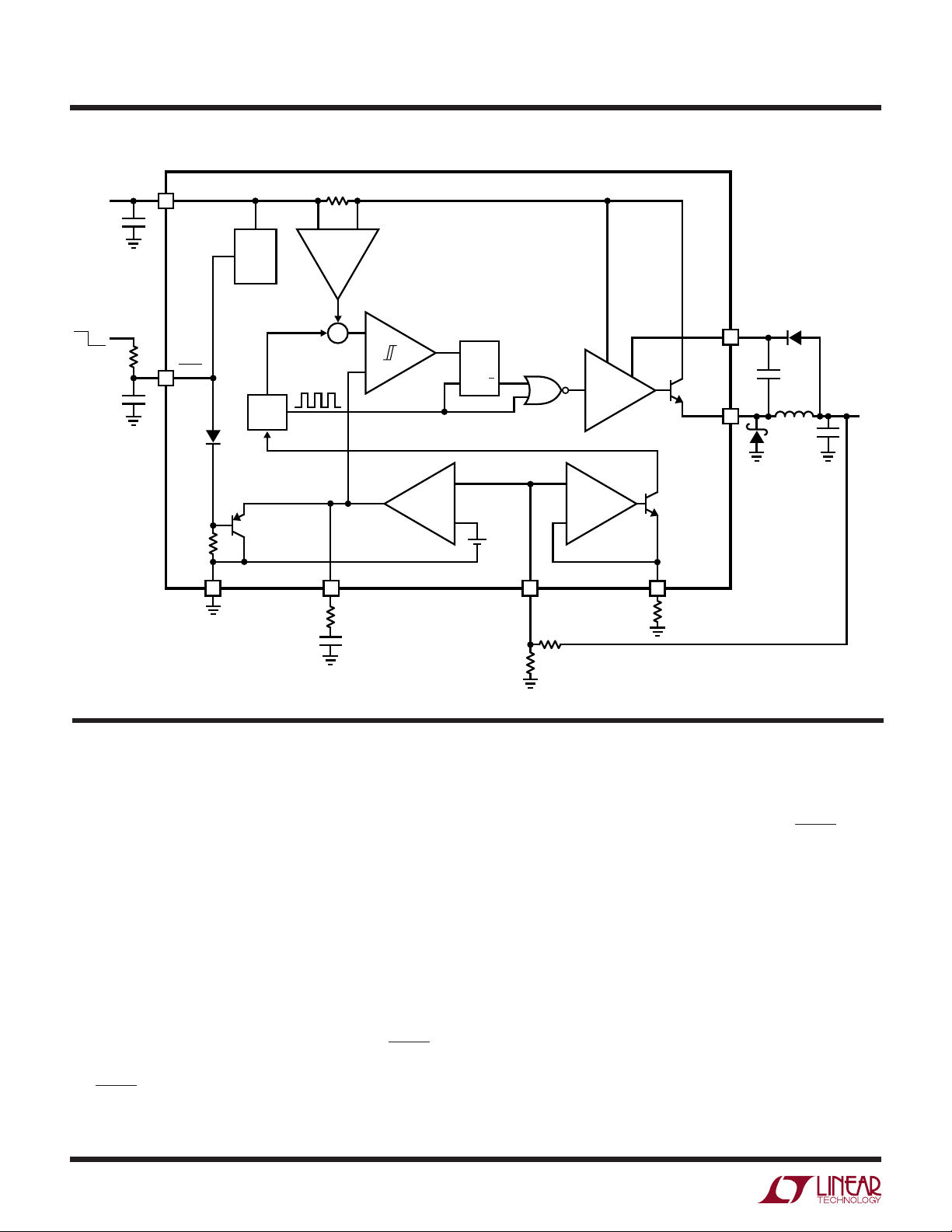
BLOCK DIAGRAM
V
IN
V
IN
3
C2
INT REG
AND
UVLO
ON OFF
R3
SHDN
4
C4
OPERATION
SLOPE
COMP
OSC
GND
5
Σ
8
(Refer to Block Diagram)
BOOST
1
Q
R
Q
S
V
C
V
C
g
m
780mV
FB
7
R1
R2
DRIVER
FREQUENCY
FOLDBACK
Q1
SW
2
R
T
6
D2
C3
L1
C1
D1
3505 BD
V
OUT
The LT3505 is a constant frequency, current mode stepdown regulator. A resistor-programmed oscillator enables
an RS fl ip-fl op, turning on the internal 1.4A power switch
Q1. An amplifi er and comparator monitor the current
fl owing between the V
and SW pins, turning the switch
IN
off when this current reaches a level determined by the
voltage at the V
pin. An error amplifi er measures the
C
output voltage through an external resistor divider tied to
the FB pin and servos the V
node. If the error amplifi er’s
C
output increases, more current is delivered to the output;
if it decreases, less current is delivered. An active clamp
(not shown) on the V
node is also clamped to the voltage on the SHDN pin;
V
C
node provides current limit. The
C
soft-start is implemented by generating a voltage ramp at
the SHDN pin using an external resistor and capacitor.
8
An internal regulator provides power to the control circuitry.
This regulator includes an undervoltage lockout to prevent
switching when V
is less than ~3.4V. The SHDN pin is
IN
used to place the LT3505 in shutdown, disconnecting the
output and reducing the input current to less than 2µA.
The switch driver operates from either the input or from
the BOOST pin. An external capacitor and diode are used
to generate a voltage at the BOOST pin that is higher than
the input supply. This allows the driver to fully saturate
the internal bipolar NPN power switch for effi cient operation.
When the FB pin is low, the voltage at the R
pin decreases
T
to reduce the oscillator frequency. This frequency foldback
helps to control the output current during start-up and
overload.
3505fc
 Loading...