

Page 1
LT3092
200mA 2-Terminal
Programmable Current Source
FEATURES
n
Programmable 2-Terminal Current Source
n
Maximum Output Current: 200mA
n
Wide Input Voltage Range: 1.2V to 40V
n
Input/Output Capacitors Not Required
n
Resistor Ratio Sets Output Current
n
Initial Set Pin Current Accuracy: 1%
n
Reverse-Voltage Protection
n
Reverse-Current Protection
n
<0.001%/V Line Regulation Typical
n
Current Limit and Thermal Shutdown Protection
n
Available in 8-Lead SOT-23, 3-Lead SOT-223 and
8-Lead 3mm × 3mm DFN Packages
APPLICATIONS
n
2-Terminal Floating Current Source
n
GND Referred Current Source
n
Variable Current Source
n
In-Line Limiter
n
Intrinsic Safety Circuits
DESCRIPTION
The LT®3092 is a programmable 2-terminal current
source. It requires only two resistors to set an output
current between 0.5mA and 200mA. A multitude of analog
techniques lend themselves to actively programming the
output current. The LT3092 is stable without input and
output capacitors, offering high DC and AC impedance. This
feature allows operation in intrinsically safe applications.
The SET pin features 1% initial accuracy and low temperature coeffi cient. Current regulation is better than
10ppm/V from 1.5V to 40V.
The LT3092 can operate in a 2-terminal current source
confi guration in series with signal lines. It is ideal for driving sensors, remote supplies, and as a precision current
limiter for local supplies.
Internal protection circuitry includes reverse-battery and
reverse-current protection, current limiting and thermal
limiting. The LT3092 is offered in the 8-lead TSOT-23,
3-lead SOT-223 and 8-lead 3mm × 3mm DFN packages.
L, LT, LTC, LTM, Linear Technology and the Linear logo are registered trademarks of Linear
Technology Corporation. All other trademarks are the property of their respective owners.
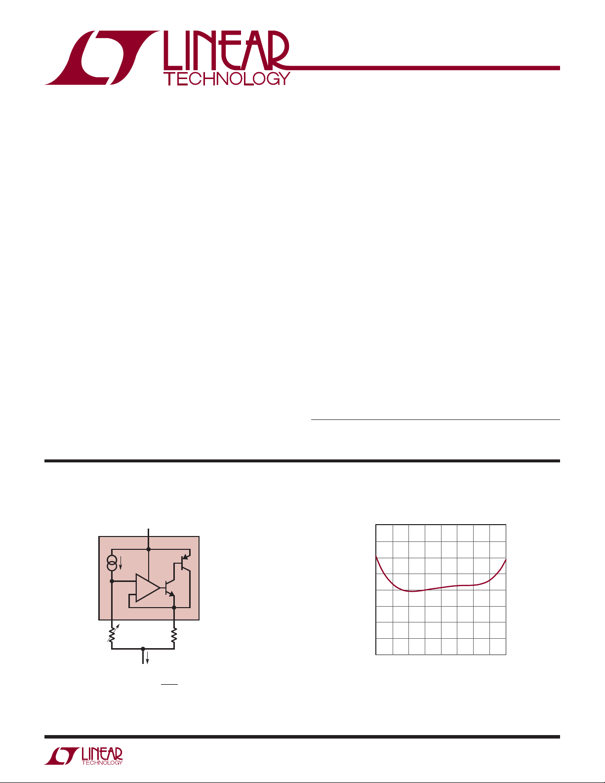
TYPICAL APPLICATION
Adjustable 2-Terminal Current Source
VIN – V
LT3092
IµA
SOURCE
= 1.2V TO 40V
OUT
IN
10µA
+
–
SET OUT
R
SET
= 10 •
R
R
SET
R
OUT
OUT
3092 TA01a
SET Pin Current vs Temperature
10.100
10.075
10.050
10.025
10.000
9.975
SET PIN CURRENT (µA)
9.950
9.925
9.900
–50
–25
25 50 10075 125
0
TEMPERATURE (°C)
150
3092 TA01b
3092fb
1
Page 2
LT3092
ABSOLUTE MAXIMUM RATINGS
(Note 1) All Voltages Relative to V
IN Pin Voltage Relative to SET, OUT ........................±40V
SET Pin Current (Note 6) .....................................±15mA
SET Pin Voltage (Relative to OUT, Note 6) ...............±10V
Output Short-Circuit Duration .......................... Indefi nite
PIN CONFIGURATION
TOP VIEW
1OUT
OUT
2
NC
3
SET
4
8-LEAD (3mm s 3mm) PLASTIC DFN
T
= 125°C, θJA = 28°C/W, θJC = 10°C/W
JMAX
EXPOSED PAD (PIN 9) IS OUT, MUST BE SOLDERED TO OUT
ON THE PCB. SEE THE APPLICATIONS INFORMATION SECTION.
9
DD PACKAGE
8
IN
IN
7
NC
6
NC
5
TAB IS OUT
T
= 125°C, θJA = 24°C/W, θJC = 15°C/W
JMAX
TAB IS OUT, MUST BE SOLDERED TO OUT ON THE PCB.
SEE THE APPLICATIONS INFORMATION SECTION.
OUT
Operating Junction Temperature Range (Notes 2, 8)
E, I Grades ......................................... –40°C to 125°C
MP Grade ........................................... –55°C to 125°C
Storage Temperature Range ................... –65°C to 150°C
Lead Temperature (ST, TS8 Packages Only)
Soldering, 10 sec .............................................. 300°C
TOP VIEW
3
2
1
ST PACKAGE
3-LEAD PLASTIC SOT-223
IN
OUT
SET
T
OUT 2
OUT 3
OUT 4
JMAX
TOP VIEW
NC 1
TS8 PACKAGE
8-LEAD PLASTIC TSOT-23
= 125°C, θJA = 57°C/W, θJC = 15°C/W
8 IN
7 IN
6 NC
5 SET
ORDER INFORMATION
LEAD FREE FINISH TAPE AND REEL PART MARKING* PACKAGE DESCRIPTION TEMPERATURE RANGE
LT3092EDD#PBF LT3092EDD#TRPBF LFJD
LT3092IDD#PBF LT3092IDD#TRPBF LFJD
8-Lead (3mm × 3mm) Plastic DFN
8-Lead (3mm × 3mm) Plastic DFN
LT3092EST#PBF LT3092EST#TRPBF 3092 3-Lead Plastic SOT-223 –40°C to 125°C
LT3092IST#PBF LT3092IST#TRPBF 3092 3-Lead Plastic SOT-223 –40°C to 125°C
LT3092MPST#PBF LT3092MPST#TRPBF 3092MP 3-Lead Plastic SOT-223 –55°C to 125°C
LT3092ETS8#PBF LT3092ETS8#TRPBF LTFJW 8-Lead Plastic SOT-23 –40°C to 125°C
LT3092ITS8#PBF LT3092ITS8#TRPBF LTFJW 8-Lead Plastic SOT-23 –40°C to 125°C
LEAD BASED FINISH TAPE AND REEL PART MARKING* PACKAGE DESCRIPTION TEMPERATURE RANGE
LT3092EDD LT3092EDD#TR LFJD
LT3092IDD LT3092IDD#TR LFJD
8-Lead (3mm × 3mm) Plastic DFN
8-Lead (3mm × 3mm) Plastic DFN
LT3092EST LT3092EST#TR 3092 3-Lead Plastic SOT-223 –40°C to 125°C
LT3092IST LT3092IST#TR 3092 3-Lead Plastic SOT-223 –40°C to 125°C
LT3092MPST LT3092MPST#TR 3092MP 3-Lead Plastic SOT-223 –55°C to 125°C
LT3092ETS8 LT3092ETS8#TR LTFJW 8-Lead Plastic SOT-23 –40°C to 125°C
LT3092ITS8 LT3092ITS8#TR LTFJW 8-Lead Plastic SOT-23 –40°C to 125°C
Consult LTC Marketing for parts specifi ed with wider operating temperature ranges. *The temperature grade is identifi ed by a label on the shipping container.
For more information on lead free part marking, go to:
For more information on tape and reel specifi cations, go to:
http://www.linear.com/leadfree/
http://www.linear.com/tapeandreel/
–40°C to 125°C
–40°C to 125°C
–40°C to 125°C
–40°C to 125°C
3092fb
2
Page 3
LT3092
ELECTRICAL CHARACTERISTICS
The l denotes the specifi cations which apply over the full operating
temperature range, otherwise specifi cations are at T
PARAMETER CONDITIONS MIN TYP MAX UNITS
SET Pin Current I
Offset Voltage (V
OUT
– V
) V
SET
Current Regulation (Note 7) ∆I
∆V
Line Regulation ∆I
∆V
Minimum Load Current (Note 3) 2V ≤ V
Dropout Voltage (Note 4) I
Current Limit VIN = 5V, V
Reference Current RMS Output Noise (Note 5) 10Hz ≤ f ≤ 100kHz 0.7 nA
Ripple Rejection f = 120Hz, V
Thermal Regulation I
SET
OS
SET
OS
SET
OS
SET
= 25°C. (Note 2)
J
VIN = 2V, I
2V ≤ V
VIN = 2V, I
V
= 2V, I
IN
∆I
LOAD
∆I
LOAD
∆VIN = 2V to 40V, I
∆V
= 2V to 40V, I
IN
= 10mA
LOAD
I
= 200mA
LOAD
C
= 0.1µF, C
SET
f = 10kHz
f = 1MHz
= 1mA
LOAD
≤ 40V, 1mA ≤ I
IN
= 1mA
LOAD
= 1mA
LOAD
= 1mA to 200mA
= 1mA to 200mA
LOAD
LOAD
≤ 40V
IN
= 0V, V
SET
RIPPLE
OUT
OUT
= 0.5V
= 2.2µF
LOAD
= 1mA
= 1mA
= –0.1V
, I
P-P
≤ 200mA
= 0.1A,
LOAD
9.9
l
9.8
10
10
10.1
10.2
–2
l
–4
–0.1
l
l
l
l
l
200 300 mA
–0.5 –2
0.03
0.003
0.2
0.010
300 500 µA
1.22
1.3
1.45
1.65
90
75
20
µA
µA
2
4
mV
mV
nA
mV
nA/V
mV/V
RMS
dB
dB
dB
10ms Pulse 0.003 %/ W
V
V
Note 1: Stresses beyond those listed under Absolute Maximum Ratings
may cause permanent damage to the device. Exposure to any Absolute
Maximum Rating condition for extended periods may affect device
reliability and lifetime.
Note 2: Unless otherwise specifi ed, all voltages are with respect to V
OUT
.
The LT3092E is tested and specifi ed under pulse load conditions such
that T
≅ TA. The LT3092E is 100% tested at TA = 25°C. Performance at
J
–40°C and 125°C is assured by design, characterization, and correlation
with statistical process controls. The LT3092I is guaranteed to meet all
data sheet specifi cations over the full –40°C to 125°C operating junction
temperature range. The LT3092MP is 100% tested and guaranteed over
the –55°C to 125°C operating junction temperature range.
Note 3: Minimum load current is equivalent to the quiescent current of
the part. Since all quiescent and drive current is delivered to the output
of the part, the minimum load current is the minimum current required to
maintain regulation.
Note 4: For the LT3092, dropout is specifi ed as the minimum input-tooutput voltage differential required supplying a given output current.
Note 5: Adding a small capacitor across the reference current resistor
lowers output noise. Adding this capacitor bypasses the resistor shot noise
and reference current noise (see the Applications Information section).
Note 6: Diodes with series 1k resistors clamp the SET pin to the OUT pin.
These diodes and resistors only carry current under transient overloads.
Note 7: Current regulation is Kelvin-sensed at the package.
Note 8: This IC includes overtemperature protection that protects the
device during momentary overload conditions. Junction temperature
exceeds the maximum operating junction temperature when
overtemperature protection is active. Continuous operation above the
specifi ed maximum operating junction temperature may impair device
reliability.
3092fb
3
Page 4

LT3092
TYPICAL PERFORMANCE CHARACTERISTICS
SET Pin Current SET Pin Current Distribution
10.100
10.075
10.050
10.025
10.000
9.975
SET PIN CURRENT (μA)
9.950
9.925
9.900
–50
–25 25
0
50
TEMPERATURE (°C)
75
100
125
150
3092 G01
N = 1326
9.80
9.90
SET PIN CURRENT DISTRIBUTION (µA)
Offset Voltage Distribution
N = 1326
–2
–1
VOS DISTRIBUTION (mV)
0
1
2
3092 G04
10
10.10
Offset Voltage
1.00
I
OUT
0.75
0.50
0.25
0
–0.25
OFFSET VOLTAGE (mV)
–0.50
–0.75
–1.00
0
Offset Voltage (V
2.0
1.5
1.0
0.5
0.0
–0.5
OFFSET VOLTAGE (mV)
–1.0
–1.5
10.20
3092 G02
= 1mA
5
10
INPUT-TO-OUTPUT VOLTAGE (V)
–2.0
–50
–25
15 20 3025 35
– V
OUT
25 50 10075 125
0
TEMPERATURE (°C)
40
3092 G05
SET
)
150
3092 G03
4
Offset Voltage
100
50
0
–50
–100
–150
–200
–250
OFFSET VOLTAGE (μV)
–300
–350
–400
0
50 150 200
100
LOAD CURRENT (mA)
3092 G06
Current Regulation
20
∆I
= 1mA TO 200mA
OUT
10
– V
V
0
–10
–20
–30
–40
WITH LOAD (nA)
–50
–60
CHANGE IN REFERENCE CURRENT
–70
–80
–50
= 3V
IN
OUT
–25 25
0
TEMPERATURE (oC)
50
125
100
75
150
3092 G07
3092fb
Page 5

TYPICAL PERFORMANCE CHARACTERISTICS
LT3092
Minimum Output Current
600
500
400
300
200
100
MINIMUM OUTPUT CURRENT (μA)
0
–50
–25 25
0
50
TEMPERATURE (°C)
Current Limit
400
350
300
250
200
150
CURRENT LIMIT (mA)
100
50
0
0
INPUT-TO-OUTPUT DIFFERENTIAL VOLTAGE (V)
Dropout Voltage Dropout Voltage
1.6
1.4
) (V)
OUT
– V
IN
DROPOUT VOLTAGE (V
125
100
75
150
3092 G08
1.2
1.0
0.8
0.6
0.4
0.2
0
0
TJ = –55°C
TJ = 25°C
TJ = 125°C
25
50
LOAD CURRENT (mA)
75 100 150125 175
200
3092 G09
1.4
1.2
) (V)
OUT
1.0
– V
IN
0.8
0.6
0.4
0.2
DROPOUT VOLTAGE (V
0
–50
–25 25
0
I
LOAD
I
LOAD
50
TEMPERATURE (°C)
75
= 200mA
= 100mA
100
125
150
3092 G10
Current Limit
500
450
400
350
300
250
200
150
CURRENT LIMIT (mA)
100
VIN = 7V
50
= 0V
V
TJ = 25°C
2
6810
4
3092 G11
OUT
0
–50
–25 25
0
TEMPERATURE (°C)
125
50
100
75
150
3092 G12
Line Transient Response Line Transient Response
8
6
4
2
INPUT VOLTAGE (V)
0
20
0
10
1mA CURRENT SOURCE
CONFIGURATION
40
30
50
TIME (µs)
1.5
1.0
OUTPUT CURRENT
0.5
DEVIATION (mA)
0
–0.5
–1.0
100
60
90
80
70
3092 G13
10
8
6
4
INPUT VOLTAGE (V)
2
0
20
10
10mA CURRENT SOURCE
CONFIGURATION
40
30
50
TIME (µs)
10
OUTPUT CURRENT
5
DEVIATION (mA)
0
–5
–10
100
60
90
80
70
3092 G14
3092fb
5
Page 6
LT3092
TYPICAL PERFORMANCE CHARACTERISTICS
8
6
4
2
INPUT VOLTAGE (V)
0
0
10
5
1mA CURRENT SOURCE
CONFIGURATION
20
15
25
TIME (µs)
Residual Output for Less Than
Minimum Output Current
800
SET PIN = 0V
700
600
500
400
300
OUTPUT VOLTAGE (mV)
200
100
0
0
V
IN
V
OUT
R
TEST
R
()
TEST
CURRENT (mA)
1.0
OUTPUT
0.5
0
50
35
VIN = 36V
VIN = 5V
45
40
3092 G15
20001000
3092 G17
30
8
6
4
2
INPUT VOLTAGE (V)
0
0
1G
100M
10M
1M
100k
10k
1k
OUTPUT IMPEDANCE ()
100
10
1
Turn-On ResponseTurn-On Response
10mA CURRENT SOURCE
CONFIGURATION
20
15
10
5
25
TIME (µs)
Output Impedance
I
= 1mA
SOURCE
I
=
SOURCE
10mA
I
= 100mA
SOURCE
100 1k 10k 100k 1M 10M10
FREQUENCY (Hz)
15
CURRENT (mA)
10
OUTPUT
5
0
50
30
45
40
35
3092 G16
3092 G18
6
Noise Spectral Density
100
10
1
REFERENCE CURRENT
0.1
NOISE SPECTRAL DENSITY (pA/√Hz)
0.01
FREQUENCY (Hz)
10k 100k10010 1k
3092 G19
3092fb
Page 7

LT3092
PIN FUNCTIONS
(DD/ST/TS8)
IN (Pins 7, 8/Pin 3/Pins 7, 8): Input. This pin supplies
power to bias internal circuitry and supply output load
current. For the device to operate properly and regulate,
the voltage on this pin must be 1.2V to 1.4V above the
OUT pin (depending on output load current—see the
dropout voltage specifi cations in the Electrical Characteristics table).
NC (Pins 3, 5, 6/NA/Pins 1, 6): No Connection. These
pins have no connection to internal circuitry and may be
tied to IN, OUT, GND or fl oated.
OUT (Pins 1, 2/Pin 2/Pins 2, 3, 4): Output. This is the
power output of the device. The minimum current source
value to which the LT3092 can be set is 0.5mA or the
device will not regulate.
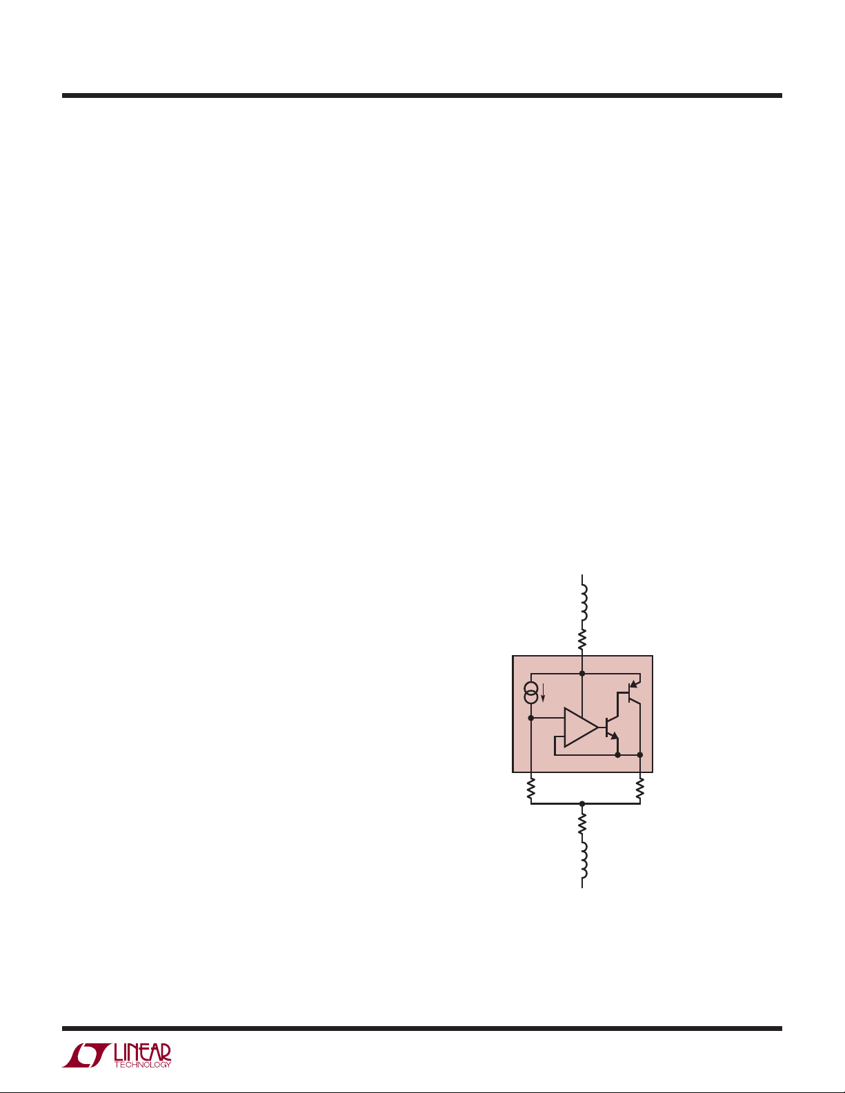
BLOCK DIAGRAM
SET (Pin 4/Pin 1/Pin 5): Set. This pin is the error amplifi er’s noninverting input and also sets the operating bias
point of the circuit. A fi xed 10A current source fl ows out
of this pin. Two resistors program I
as a function of
OUT
the resistor ratio relative to 10A. Output current range
is 0.5mA to the maximum rated 200mA level.
Exposed Pad/Tab (Pin 9/Tab/NA): Output. The Exposed
Pad of the DFN package and the Tab of the SOT-223
package are tied internally to OUT. Tie them directly to
the OUT pins (Pins 1, 2/Pin 2) at the PCB. The amount
of copper area and planes connected to OUT determine
the effective thermal resistance of the packages (see the
Applications Information section).
SET
IN
10µA
+
–
OUT
3092 BD
3092fb
7
Page 8

LT3092
APPLICATIONS INFORMATION
Introduction
The LT3092 is a versatile IC that operates as a 2-terminal
programmable current source with the addition of only
two external resistors; no external bypass capacitors are
needed for stability.
The LT3092 is easy to use and has all the protection features expected in high performance products. Included
are reverse-voltage protection, reverse-current protection, short-circuit protection and thermal shutdown with
hysteresis.
The LT3092 operates with or without input and output
capacitors. The simplest current source application
requires only two discrete resistors to set a constant
output current up to 200mA. A variety of analog techniques lend themselves to regulating and varying the
current source value.
The device utilizes a precision “0” TC 10A reference current source to program output current. This 10µA current
source connects to the noninverting input of a power
operational amplifi er. The power operational amplifi er
provides a low impedance buffered output of the voltage
on the noninverting input.
Many application areas exist in which operation without
input and output capacitors is advantageous. A few of
these applications include sensitive circuits that cannot
endure surge currents under fault or overload conditions
and intrinsic safety applications in which safety regulations
limit energy storage devices that may spark or arc.
Programming Output Current in 2-Terminal
Current Source Mode
With a 10A current source generating the reference that
gains up to set output current, leakage paths to or from
the SET pin can create errors in the reference and output
currents. High quality insulation should be used (e.g.,
Tefl on, Kel-F). The cleaning of all insulating surfaces to
remove fl uxes and other residues may be required. Surface
coating may be necessary to provide a moisture barrier
in high humidity environments.
Minimize board leakage by encircling the SET pin and
circuitry with a guard ring operated at a potential close
to itself; tie the guard ring to the OUT pin. Guarding
both sides of the circuit board is required. Bulk leakage
reduction depends on the guard ring width. Ten nanoamperes of leakage into or out of the SET pin and its associated circuitry creates a 0.1% reference current error.
Leakages of this magnitude, coupled with other sources
of leakage, can cause signifi cant offset voltage and reference current drift, especially over the possible operating
temperature range.
10µA
and R
IN
ImA
≥
05
.
+
–
I
OUT
OUT
OUT
VµAR
SET SET
I
OUT
R
OUT
3092 F01
=
10
•
V
==
R
SET
OUT
10
µA
R
•
OUT
RR
SET
LT3092
+
V
SET
–
Figure 1. Using the LT3092 as a Current Source
Selecting R
SET OUT
R
SET
SET
Setting the LT3092 to operate as a 2-terminal current
source is a simple matter. The 10µA reference current from
the SET pin is used with one resistor to generate a small
voltage, usually in the range of 100mV to 1V (200mV is
a level that will help reject offset voltage, line regulation,
and other errors without being excessively large). This
voltage is then applied across a second resistor that
connects from OUT to the fi rst resistor. Figure 1 shows
connections and formulas to calculate a basic current
source confi guration.
8
In Figure 1, both resistors R
SET
and R
program the
OUT
value of the output current. The question now arises: the
ratio of these resistors is known, but what value should
each resistor be?
The fi rst resistor to select is R
. The value selected should
SET
generate enough voltage to minimize the error caused by
the offset between the SET and OUT pins. A reasonable
(R
starting level is 200mV of voltage across R
SET
SET
equal
to 20k). Resultant errors due to offset voltage are a few
percent. The lower the voltage across R
becomes, the
SET
higher the error term due to the offset.
3092fb
Page 9
APPLICATIONS INFORMATION
LT3092
From this point, selecting R
forward calculation from R
is easy, as it is a straight-
OUT
. Take note, however, resistor
SET
errors must be accounted for as well. While larger voltage
drops across R
minimize the error due to offset, they
SET
also increase the required operating headroom.
Obtaining the best temperature coeffi cient does not require
the use of expensive resistors with low ppm temperature
coeffi cients. Instead, since the output current of the LT3092
is determined by the ratio of R
SET
to R
, those resistors
OUT
should have matching temperature characteristics. Less
expensive resistors made from the same material will
provide matching temperature coeffi cients. See resistor
manufacturers’ data sheets for more details.
Stability and Frequency Compensation
The LT3092 does not require input or output capacitors
for stability in many current-source applications. Clean,
tight PCB layouts provide a low reactance, well controlled
operating environment for the LT3092 without requiring
capacitors to frequency-compensate the circuit. The front
page Typical Application circuit illustrates the simplicity
of using the LT3092.
Some current source applications will use a capacitor
connected in parallel with the SET pin resistor to lower
the current source’s noise. This capacitor also provides a
soft-start function for the current source. This capacitor
connection is depicted in Figure 7 (see the Quieting the
Noise section).
When operating with a capacitor across the SET pin resistor, external compensation is usually required to maintain
stability and compensate for the introduced pole. The
following paragraphs discuss methods for stabilizing
the LT3092 for either this capacitance or other complex
impedances that may be presented to the device. Linear
Technology strongly recommends testing stability in situ
with fi nal components before beginning production.
inductive components and may be complex distributed
networks. In addition, the current source’s value will differ between applications and its connection may be GND
referenced, power supply referenced or fl oating in a signal
line path. Linear Technology strongly recommends that
stability be tested in situ for any LT3092 application.
In LT3092 applications with long wires or PCB traces, the
inductive reactance may cause instability. In some cases,
adding series resistance to the input and output lines (as
shown in Figure 2) may suffi ciently dampen these possible
high-Q lines and provide stability. The user must evaluate
the required resistor values against the design’s headroom
constraints. In general, operation at low output current
levels (< 5mA) automatically requires higher values of
programming resistors and may provide the necessary
damping without additional series impedance.
If the line impedances in series with the LT3092 are
complex enough such that series damping resistors are
not suffi cient, a frequency compensation network may be
necessary. Several options may be considered.
LONG LINE
REACTANCE/INDUCTANCE
R
SERIES
10µA
SET
IN
+
–
R
SERIES
LONG LINE
REACTANCE/INDUCTANCE
R
OUT
3092 F02
LT3092
SET OUT
R
Although the LT3092’s design strives to be stable without
any capacitors over a wide variety of operating conditions,
it is not possible to test for all possible combinations of
input and output impedances that the LT3092 will encounter.
These impedances may include resistive, capacitive and
Figure 2. Adding Series Resistor Decouples
and Dampens Long Line Reactances
3092fb
9
Page 10

LT3092
APPLICATIONS INFORMATION
Figure 3 depicts the simplest frequency compensation
network as a single capacitor connected across the two
terminals of the current source. In this case, either a
capacitor with a value less than 1000pF, or greater than
1µF (ESR < 0.5), may stabilize the circuit. Some applications may use the small value capacitor to stand
off DC voltage, but allow the transfer of data down a
signal line.
For some applications, this capacitance range may be
unacceptable or present a design constraint. One circuit
example typifying this is an “intrinsically-safe” circuit in
which an overload or fault condition potentially allows
the capacitor’s stored energy to create a spark or arc.
For applications in which a single capacitor is unacceptable,
Figure 3 alternately shows a series RC network connected
across the two terminals of the current source. This network
has two benefi ts. First, it limits the potential discharge
current of the capacitor under a fault condition, preventing
sparks or arcs. Second, it bridges the gap between the
upper bound of 1000pF for small capacitors to the lower
bound of 1µF for large capacitors such that almost any
value capacitor can be used. This allows the user greater
fl exibility for frequency compensating the loop and fi ne
tuning the RC network for complex impedance networks.
In many instances, a series RC network is the best solution
for stabilizing the application circuit. Typical resistor values
will range from 100 to about 5k, especially for capacitor
values in between 1000pF and 1µF. Once again, Linear
Technology strongly recommends testing stability in situ
for any LT3092 application across all operating conditions,
especially ones that present complex impedance networks
at the input and output of the current source.
If an application refers the bottom of the LT3092 current
source to GND, it may be necessary to bypass the top
of the current source with a capacitor to GND. In some
cases, this capacitor may already exist and no additional
capacitance is required. For example, if the LT3092 was
used as a variable current source on the output of a power
supply, the output bypass capacitance would suffi ce to
provide LT3092 stability. Other applications may require
the addition of a bypass capacitor. Once again, the same
capacitor value requirements previously mentioned apply
in that an upper bound of 1000pF exists for small values
of capacitance, and a lower bound of 1µF (ESR < 0.5)
exists for large value capacitors. A series RC network may
also be used as necessary, and depends on the application
requirements.
In some extreme cases, capacitors or series RC networks
may be required on both the LT3092’s input and output to
stabilize the circuit. Figure 4 depicts a general application
using input and output capacitor networks, rather than
an input-to-output capacitor. As the input of the current
source tends to be high impedance, placing a capacitor
on the input does not have the same effect as placing a
10
10µA
SET
IN
C
COMP
+
–
R
OUT
3092 F03
R
OR
LT3092
SET OUT
R
Figure 3. Compensation From Input to
Output of Current Source Provides Stability
COMP
C
COMP
V
IN
R
LT3092
IN
C
IN
SET OUT
3092 F04
Figure 4. Input and/or Output Capacitors May
Be Used for Compensation
IN
10µA
+
–
R
SET
R
OUT
I
OUT
C
OR
OUT
R
OUT
C
OUT
3092fb
Page 11

APPLICATIONS INFORMATION
LT3092
capacitor on the lower impedance output, and the same
restrictions do not apply. Capacitors in the range of 0.1µF
to 1µF usually provide suffi cient bypassing on the input,
and the value of input capacitance may be increased
without limit.
If an application uses GND referred capacitors on the input
or output (particularly the input), pay attention to the length
of the lines powering and returning ground from the circuit.
In the case where long power supply and return lines are
coupled with low ESR input capacitors, application-specifi c
voltage spikes, oscillations and reliability concerns may
be seen. This is not an issue with LT3092 stability, but
rather the low ESR capacitor forming a high-Q resonant
tank circuit with the inductance of the input wires. Adding
series resistance with the input of the LT3092, or with the
input capacitor, often solves this. Resistor values of 0.1
to 1 are often suffi cient to dampen this resonance.
Give extra consideration to the use of ceramic capacitors.
Ceramic capacitors are manufactured with a variety of dielectrics, each with different behavior across temperature
and applied voltage. The most common dielectrics used
are specifi ed with EIA temperature characteristic codes of
Z5U, Y5V, X5R and X7R. The Z5U and Y5V dielectrics are
good for providing high capacitances in a small package,
but they tend to have strong voltage and temperature
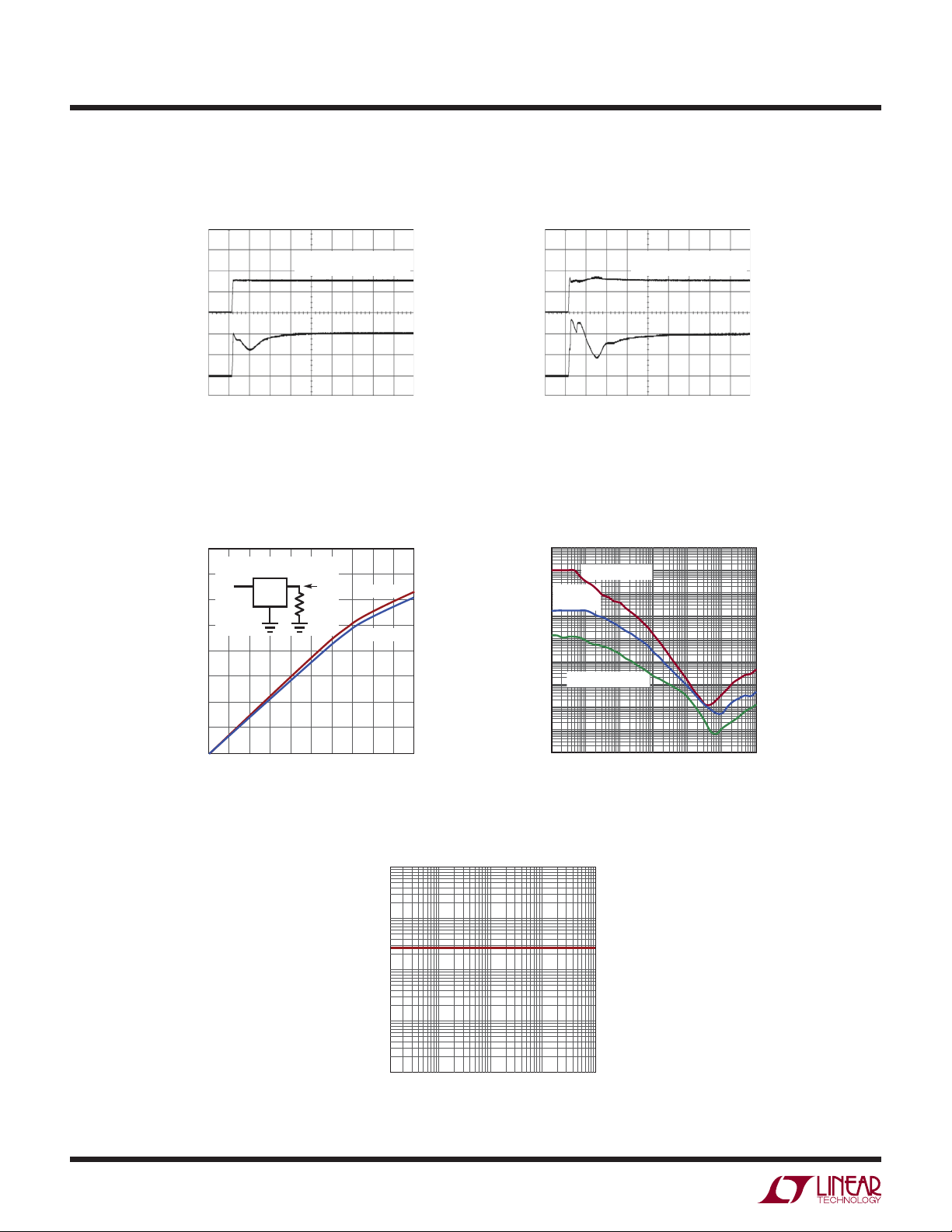
coeffi cients as shown in Figures 5 and 6. When used with
a 5V regulator, a 16V 10F Y5V capacitor can exhibit an
effective value as low as 1F to 2F for the DC bias voltage
applied and over the operating temperature range. The X5R
and X7R dielectrics result in more stable characteristics
and are more suitable for use as the output capacitor.
The X7R type has better stability across temperature,
while the X5R is less expensive and is available in higher
values. Care still must be exercised when using X5R and
X7R capacitors; the X5R and X7R codes only specify
operating temperature range and maximum capacitance
change over temperature. Capacitance change due to DC
bias with X5R and X7R capacitors is better than Y5V and
Z5U capacitors, but can still be signifi cant enough to drop
capacitor values below appropriate levels. Capacitor DC
bias characteristics tend to improve as component case
size increases, but expected capacitance at operating
voltage should be verifi ed.
Voltage and temperature coeffi cients are not the only
sources of problems. Some ceramic capacitors have a
piezoelectric response. A piezoelectric device generates
voltage across its terminals due to mechanical stress. In a
ceramic capacitor the stress can be induced by vibrations
in the system or thermal transients.
20
0
–20
–40
–60
CHANGE IN VALUE (%)
–80
–100
0
26
Figure 5. Ceramic Capacitor DC Bias Characteristics
BOTH CAPACITORS ARE 16V,
1210 CASE SIZE, 10µF
X5R
Y5V
4
8
DC BIAS VOLTAGE (V)
10
14
12
16
3092 F05
40
20
0
–20
–40
–60
CHANGE IN VALUE (%)
–80
BOTH CAPACITORS ARE 16V,
1210 CASE SIZE, 10µF
–100
–50
–25 0
Figure 6. Ceramic Capacitor Temperature Characteristics
25 75
TEMPERATURE (°C)
X5R
Y5V
50 100 125
3092 F06
3092fb
11
Page 12

LT3092
APPLICATIONS INFORMATION
Quieting the Noise
When a reduction in the noise of the current source is
(C
desired, a small capacitor can be placed across R
SET
SET
in Figure 7). Normally, the 10µA reference current source
generates noise current levels of 2.7pA/√Hz (0.7nA
RMS
over the 10Hz to 100kHz bandwidth). The SET pin resistor
generates a spot noise equal to i
–23
constant, 1.38 • 10
J/°K, and T is absolute temperature)
= √4kT/R (k = Boltzmann’s
n
which is RMS-summed with the noise generated by the
10µA reference current source. Placing a C
across R
(as shown in Figure 7) bypasses this noise
SET
capacitor
SET
current. Note that this noise reduction capacitor increases
start-up time as a factor of the time constant formed by
• C
R
SET
. When using a capacitor across the SET pin
SET
resistor, the external pole introduced usually requires
compensation to maintain stability. See the Stability and
Frequency Compensation section for detailed descriptions
on compensating LT3092 circuits.
A curve in the Typical Performance Characteristics section
depicts noise spectral density for the reference current
over a 10Hz to 100kHz bandwidth.
Paralleling Devices
Obtain higher output current by paralleling multiple
LT3092’s together. The simplest application is to run
two current sources side by side and tie their inputs
together and their outputs together, as shown in Figure
8. This allows the sum of the current sources to deliver
more output current than a single device is capable of
delivering.
Another method of paralleling devices requires fewer
components and helps to share power between devices.
Tie the individual SET pins together and tie the individual
IN pins together. Connect the outputs in common using
small pieces of PC trace as ballast resistors to promote
equal current sharing. PC trace resistance in milliohms/
inch is shown in Table 1. Ballasting requires only a tiny
area on the PCB.
Table 1. PC Board Trace Resistance
WEIGHT (oz) 10mil WIDTH 20mil WIDTH
1 54.3 27.1
2 27.1 13.6
Trace resistance is measured in m/in
10µA
IN
+
–
C
SET
LT3092
SET OUT
R
SET
Figure 7. Adding C
C
COMP
R
OUT
3092 F07
Lowers Current Noise
SET
OR
R
COMP
C
COMP
The worst-case room temperature offset, only ±2mV between the SET pin and the OUT pin, allows the use of very
small ballast resistors.
As shown in Figure 9, each LT3092 has a small 40m
ballast resistor, which at full output current gives better
than 80% equalized sharing of the current. The external
resistance of 40m (20m for the two devices in parallel) only adds about 8mV of output voltage compliance at
an output of 0.4A. Of course, paralleling more than two
LT3092’s yields even higher output current. Spreading the
device on the PC board also spreads the heat. Series input
resistors can further spread the heat if the input-to-output
difference is high.
Thermal Considerations
The LT3092’s internal power and thermal limiting circuitry
protects itself under overload conditions. For continuous
normal load conditions, do not exceed the 125°C maximum
junction temperature. Carefully consider all sources of
thermal resistance from junction-to-ambient. This includes
(but is not limited to) junction-to-case, case-to-heat sink
3092fb
12
Page 13

APPLICATIONS INFORMATION
LT3092
I
OUT
LT3092
IN IN
10µA 10µA
300 300
LT3092
+
–
SET SETOUTOUTOUTOUT
1.33 1.33
I
, 300mA
OUT
Figure 8. Connect Two LT3092s for Higher Current
I
OUT
LT3092
IN IN
10µA
+
–
SET SET
LT3092
10µA
+
–
40m*
+
–
3092 F08
40m*
20k20k
R
x
R
=
x
VR
•
IN MAX
()
%90
50k
1V
3092 F09
I
, 400mA
OUT
Figure 9. Parallel Devices
interface, heat sink resistance or circuit board-to-ambient
as the application dictates. Consider all additional, adjacent
heat generating sources in proximity on the PCB.
Surface mount packages provide the necessary heat
sinking by using the heat spreading capabilities of the
PC board, copper traces and planes. Surface mount heat
sinks, plated through-holes and solder fi lled vias can also
spread the heat generated by power devices.
Junction-to-case thermal resistance is specifi ed from the
IC junction to the bottom of the case directly, or the bottom
of the pin most directly, in the heat path. This is the lowest
thermal resistance path for heat fl ow. Only proper device
mounting ensures the best possible thermal fl ow from this
area of the package to the heat sinking material.
R
2.5
*40m PC BOARD TRACE
Note that the Exposed Pad of the DFN package and the
Tab of the SOT-223 package are electrically connected
to the output (V
OUT
).
The following tables list thermal resistance as a function
of copper areas in a fi xed board size. All measurements
were taken in still air on a four-layer FR-4 board with 1oz
solid internal planes and 2oz external trace planes with a
total fi nished board thickness of 1.6mm.
PCB layers, copper weight, board layout and thermal vias
affect the resultant thermal resistance. Please reference
JEDEC standard JESD51-7 for further information on high
thermal conductivity test boards. Achieving low thermal
resistance necessitates attention to detail and careful layout.
3092fb
13
Page 14

LT3092
APPLICATIONS INFORMATION
Demo circuit 1531A’s board layout using multiple inner
planes and multiple thermal vias achieves 28°C/W
V
OUT
performance for the DFN package.
Table 2. DD Package, 8-Lead DFN
COPPER AREA
TOPSIDE* BACKSIDE BOARD AREA
2
2500mm
1000mm
225mm
100mm
*Device is mounted on topside
Table 3. TS8 Package, 8-Lead SOT-23
COPPER AREA
TOPSIDE* BACKSIDE BOARD AREA
2500mm
1000mm
225mm
100mm
*Device is mounted on topside
2500mm22500mm
2
2500mm22500mm
2
2500mm22500mm
2
2500mm22500mm
2
2500mm22500mm
2
2500mm22500mm
2
2500mm22500mm
2
2500mm22500mm
THERMAL RESISTANCE
(JUNCTION-TO-AMBIENT)
2
2
2
2
(JUNCTION-TO-AMBIENT)
2
2
2
2
25°C/W
25°C/W
28°C/W
32°C/W
THERMAL RESISTANCE
54°C/W
54°C/W
57°C/W
63°C/W
V
IN(MAX CONTINUOUS)
V
OUT(MIN CONTINUOUS)
= 200mA
I
OUT
= 16.5 (15V + 10%)
= 11.4V (12V – 5%)
Power dissipation under these conditions equals:
P
= (16.5 – 11.4V)(200mA) = 1.02W
TOTAL
Junction temperature equals:
T
J
= TA + P
TOTAL
• θ
JA
TJ = 50°C + (1.02W • 30°C/W) = 80.6°C
In this example, the junction temperature is below the
maximum rating, ensuring reliable operation.
Protection Features
The LT3092 incorporates several protection features ideal
for battery-powered circuits, among other applications.
In addition to normal circuit protection features such as
current limiting and thermal limiting, the LT3092 protects
itself against reverse-input voltages, reverse-output voltages, and reverse OUT-to-SET pin voltages.
Table 4. ST Package, 3-Lead SOT-223
COPPER AREA
TOPSIDE* BACKSIDE BOARD AREA
2
2500mm
1000mm
225mm
100mm22500mm22500mm
*Device is mounted on topside
For further information on thermal resistance and using thermal information,
refer to JEDEC standard JESD51, notably JESD51-12.
2500mm22500mm
2
2500mm22500mm
2
2500mm22500mm
THERMAL RESISTANCE
(JUNCTION-TO-AMBIENT)
2
2
2
2
20°C/W
20°C/W
24°C/W
29°C/W
Calculating Junction Temperature
Example: Given an industrial factory application with an
input voltage of 15V ±10%, an output voltage of 12V ±5%,
an output current of 200mA and a maximum ambient
temperature of 50°C, what would be the maximum junction temperature for a DFN package?
The total circuit power equals:
P
TOTAL
= (VIN – V
OUT
)(I
OUT
)
Current limit protection and thermal overload protection
protect the IC against output current overload conditions. For normal operation, do not exceed a junction
temperature of 125°C. The thermal shutdown circuit’s
typical temperature threshold is 165°C and has about
5°C of hysteresis.
The LT3092’s IN pin withstands ±40V voltages with respect
to the SET and OUT pins. Reverse-current fl ow, if OUT is
greater than IN, is less than 1mA (typically under 100µA),
protecting the LT3092 and sensitive loads.
Clamping diodes and 1k limiting resistors protect the
LT3092’s SET pin relative to the OUT pin voltage. These
protection components typically only carry current under
transient overload conditions. These devices are sized to
handle ±10V differential voltages and ±15mA crosspin
current fl ow without concern.
The SET pin current is negligible and can be ignored.
14
3092fb
Page 15

TYPICAL APPLICATIONS
LT3092
Paralleling Current Sources for Higher Current
LT3092
IN
10µA
+
–
SET OUT
⎛
RRR
IµA
=+
10
OUT
214
•
⎜
⎝
LT3092
SET OUT
R1R2
I
⎞
OUT
⎟
R
3
⎠
IN
10µA
+
–
3092 TA02
High Voltage Current Source
10µA
IN
D1
+
35V
LT3092
–
SET OUT
R4
20k
LT3092
10µA
+
R3
2
IN
ImA
≥=05
OUT
I
OUT
D2
35V
–
R3R4
.
200
Paralleling LT3092s with Ballast Resistor
LT3092
IN
10µA
+
–
SET OUT
R2
40.2k
LT3092
SET OUT
R1
40m
400mA
IN
10µA
+
–
R3
40m
R4
2
3092 TA03
Decreasing Power Dissipation in LT3092 100mA Current Source
10µA
IN
R
OUT
3092 TA05
x
VVV
==(– )
MAX IN OUT MAX
R
x
mV
200
R
1
R1
2
V
MAX
•%
90
+
–
I
OUT
100mA
LT3092
SET
R2
20k
mV
R
1
Capacitor Adds Stability, But Limits Slew Rate
SET OUT
+
200mV
–
R2
20k
I
OUT
100mA
R1
2
3092 TA04
LT3092
SET
R2
20k
10µA
IN
C1
+
–
OUT
R1
2
3092 TA06
I
OUT
100mA
LIMIT
dV
dt
≤ 901%•
I
OUT
C
3092fb
15
Page 16

LT3092
TYPICAL APPLICATIONS
Remote Temperature Sensor
LT3092
10µA
SET OUT
49.9k 49.9
MURATA
NCP15WF104F03RC
1% 100k
Pulsed Current Source, Load to Ground
DAC Controlled Current Source
I
= 0.5mA TO
+
–
OUT
100mA
IN
10
3092 TA08
INPUT
+
V
V
IN
IN
LT3092
10µA
+
–
SET OUT
DAC OUTPUT
0V TO 1V
I
OUT
LOAD
3092 TA07
Active Load
LT3092
IN
10µA
+
–
SET OUT
1mA
10010k
OUTPUT
3092 TA09
Fully Floating Current Source Switches
From 200mA to Quiescent Current
ON
OFF
V
IN
LT3092
IN
10µA
+
–
SET OUT
20k
VN2222LL
1
I
OUT
200mA
LOAD
3092 TA10
OPTO-FET
NEC PS 7801-1A
V
IN
LT3092
IN
10µA
+
–
SET OUT
100k 4.99
200mA
3092 TA11
16
3092fb
Page 17

TYPICAL APPLICATIONS
LT3092
Pulsed Current Source, Load to V
V
IN
LOAD
I
OUT
LT3092
IN
10µA
+
–
OFF
SET
ON
OUT
120k
3092 TA12
Voltage Clamp
IN
I
OUT
2-Terminal AC Current Limiter
LT3092
10µA
+
I
OUT
–
20k
I
OUT
3092 TA13
I
OUT
I
SET
.
V
02
R
High Accuracy Current Source
V
IN
2N3906
10k
10k
10k
IN
LT3092
2N3904
SET
10µA
10µA
IN
+
–
124
0.1%
10mA
I
OUT
3092 TA15
3092fb
LT3092
+
–
100k
10V
VIN – V
OUT
4.99
3092 TA14
OUT
V
OUT
= 11V TRIP POINT
SET OUT
LT1634-1.25
17
Page 18

LT3092
TYPICAL APPLICATIONS
V
IN
2-Level Current Source
LT3092
IN
10µA
+
–
SET OUT
100k
100k*
VN2222LL*
10V*
*CURRENT FOLDBACK CIRCUIT LIMITS
THE LT3092 POWER DISSIPATION
10k*
= 200mA, IF VIN – V
I
OUT
= 100mA, IF V
4.99
V
OUT
< 12V
OUT
– V
> 12V
IN
OUT
3092 TA16
More Effi cient Current Source
V
IN
+
36V
–
V
IN
SHDN
LT3470A
GND
BOOST
SW
BIAS
0.22µF
33µH
10µA
+
–
20k
IN
1
I
OUT
C3
47µF
1nF
ZVP3306F
1k
3092 TA17
FB
LT3092
100
SET OUT
18
3092fb
Page 19

PACKAGE DESCRIPTION
DD Package
8-Lead Plastic DFN (3mm × 3mm)
(Reference LTC DWG # 05-08-1698)
0.675 ±0.05
R = 0.115
TYP
LT3092
0.38 ± 0.10
85
3.5 ±0.05
NOTE:
1. DRAWING TO BE MADE A JEDEC PACKAGE OUTLINE M0-229 VARIATION OF (WEED-1)
2. DRAWING NOT TO SCALE
3. ALL DIMENSIONS ARE IN MILLIMETERS
4. DIMENSIONS OF EXPOSED PAD ON BOTTOM OF PACKAGE DO NOT INCLUDE
MOLD FLASH. MOLD FLASH, IF PRESENT, SHALL NOT EXCEED 0.15mm ON ANY SIDE
1.65 ±0.05
(2 SIDES)2.15 ±0.05
PACKAGE
OUTLINE
0.25 ± 0.05
RECOMMENDED SOLDER PAD PITCH AND DIMENSIONS
0.50 BSC
2.38 ±0.05
(2 SIDES)
PIN 1
TOP MARK
(NOTE 6)
0.200 REF
ST Package
3-Lead Plastic SOT-223
(Reference LTC DWG # 05-08-1630)
.248 – .264
(6.30 – 6.71)
.114 – .124
(2.90 – 3.15)
3.00 ±0.10
(4 SIDES)
0.75 ±0.05
5. EXPOSED PAD SHALL BE SOLDER PLATED
6. SHADED AREA IS ONLY A REFERENCE FOR PIN 1 LOCATION
ON TOP AND BOTTOM OF PACKAGE
.059 MAX
1.65 ± 0.10
0.00 – 0.05
.129 MAX
(2 SIDES)
0.25 ± 0.05
2.38 ±0.10
(2 SIDES)
BOTTOM VIEW—EXPOSED PAD
14
0.50 BSC
(DD) DFN 1203
.264 – .287
(6.70 – 7.30)
.130 – .146
(3.30 – 3.71)
.071
(1.80)
MAX
.0905
(2.30)
BSC
.024 – .033
(0.60 – 0.84)
.181
(4.60)
BSC
.033 – .041
(0.84 – 1.04)
.012
(0.31)
MIN
.059 MAX
10o
MAX
.181 MAX
RECOMMENDED SOLDER PAD LAYOUT
10o – 16o
.0008 – .0040
(0.0203 – 0.1016)
.248 BSC
.039 MAX
.090
BSC
.010 – .014
(0.25 – 0.36)
10o – 16o
ST3 (SOT-233) 0502
3092fb
19
Page 20

LT3092
PACKAGE DESCRIPTION
TS8 Package
8-Lead Plastic TSOT-23
(Reference LTC DWG # 05-08-1637)
3.85 MAX
0.20 BSC
0.52
MAX
2.62 REF
RECOMMENDED SOLDER PAD LAYOUT
PER IPC CALCULATOR
DATUM ‘A’
NOTE:
1. DIMENSIONS ARE IN MILLIMETERS
2. DRAWING NOT TO SCALE
3. DIMENSIONS ARE INCLUSIVE OF PLATING
4. DIMENSIONS ARE EXCLUSIVE OF MOLD FLASH AND METAL BURR
0.65
REF
0.30 – 0.50 REF
1.22 REF
1.4 MIN
2.80 BSC
0.09 – 0.20
(NOTE 3)
1.50 – 1.75
(NOTE 4)
PIN ONE ID
0.65 BSC
0.80 – 0.90
1.00 MAX
5. MOLD FLASH SHALL NOT EXCEED 0.254mm
6. JEDEC PACKAGE REFERENCE IS MO-193
2.90 BSC
(NOTE 4)
0.22 – 0.36
8 PLCS (NOTE 3)
0.01 – 0.10
1.95 BSC
TS8 TSOT-23 0802
20
3092fb
Page 21

LT3092
REVISION HISTORY
REV DATE DESCRIPTION PAGE NUMBER
B 12/09 Update Order Information 2
(Revision history begins at Rev B)
Information furnished by Linear Technology Corporation is believed to be accurate and reliable.
However, no responsibility is assumed for its use. Linear Technology Corporation makes no representation that the interconnection of its circuits as described herein will not infringe on existing patent rights.
3092fb
21
Page 22

LT3092
TYPICAL APPLICATIONS
USB LED Driver
LT3092
IN
10µA
+
–
SET OUT
20k
3092 TA18
USB
1
ADJUST LIMIT
200mA LED
Current Limiter for Remote Power
V
IN
LT3092
IN
10µA
+
–
SET OUT
100k
3092 TA19
RELATED PARTS
PART NUMBER DESCRIPTION COMMENTS
LDO
LT1761 100mA, Low Noise LDO 300mV Dropout Voltage, Low Noise: 20µV
LT1762 150mA, Low Noise LDO 300mV Dropout Voltage, Low Noise: 20µV
LTC1844 150mA, Very Low Dropout LDO 80mV Dropout Voltage, Low Noise <30µV
Capacitors, ThinSOT Package
LT1962 300mA, Low Noise LDO 270mV Dropout Voltage, Low Noise: 20µV
LT1964 200mA, Low Noise, Negative LDO 340mV Dropout Voltage, Low Noise 30µV
LT3008 20mA, 45V, 3µA I
Micropower LDO 280mV Dropout Voltage, Low IQ: 3µA, VIN = 2V to 45V, V
Q
ThinSOT and 2mm × 2mm DFN-6 Packages
LT3009 20mA, 20V, 3µA IQ Micropower LDO 280mV Dropout Voltage, Low IQ: 3µA, VIN = 1.6V to 20V, V
ThinSOT and SC70 Packages
LT3020 100mA, Low Voltage VLDO Linear
Regulator
LTC3025 300mA Micropower VLDO Linear
Regulator
LTC3035 300mA VLDO Linear Regulator with
Charge Pump Bias Generator
LT3080/
LT3080-1
1.1A, Parallelable, Low Noise,
Low Dropout Linear Regulator
VIN: 0.9V to 10V, V
: 0.2V to 5V (Min), VDO = 0.15V, IQ = 120µA, Noise: <250µV
OUT
Stable with 2.2µF Ceramic Capacitors, DFN-8, MS8 Packages
VIN = 0.9V to 5.5V, Dropout Voltage: 45mV, Low Noise 80µV
2mm × 2mm DFN Package
V
= 1.7V to 5.5V, V
IN
: 0.4V to 3.6V, Dropout Voltage: 45mV, IQ: 100µA, 3mm × 2mm DFN-8
OUT
300mV Dropout Voltage (2-Supply Operation), Low Noise: 40µV
V
: 0V to 35.7V, Current-Based Reference with 1-Resistor V
OUT
(No Op Amp Required), Stable with Ceramic Caps, TO-220, SOT-223, MSOP-8 and
3mm × 3mm DFN-8 Packages; LT3080-1 Version Has Integrated Internal Ballast Resistor
LT3085 500mA, Parallelable, Low Noise, Low
Dropout Linear Regulator
275mV Dropout Voltage (2-Supply Operation), Low Noise: 40µV
V
: 0V to 35.7V, Current-based Reference with 1-Resistor V
OUT
(No Op Amp Required), Stable with Ceramic Caps, MSOP-8 and 2mm × 3mm DFN-6 Packages
Current Sense Amplifi ers
LT6106 Low Cost, 36V High Side Current
36V (44V Max) Current Sense, Dynamic Range of 2000:1, 106dB of PSRR
Sense Amplifi er
LT6107 High Temperature High Side Current
Sense Amp in SOT-23
36V (44V Max) Current Sense, Dynamic Range of 2000:1, 106dB of PSRR, –55 to 150°C
(MP-Grade)
ThinSOT is a trademark of Linear Technology Corporation.
Linear Technology Corporation
22
1630 McCarthy Blvd., Milpitas, CA 95035-7417
(408) 432-1900 ● FAX: (408) 434-0507
●
www.linear.com
, VIN = 1.8V to 20V, ThinSOT™ Package
RMS
, VIN = 1.8V to 20V, MS8 Package
RMS
, VIN = 1.6V to 6.5V, Stable with 1µF Output
RMS
, VIN = 1.8V to 20V, MS8 Package
RMS
, VIN = –1.8V to –20V, ThinSOT Package
RMS
4.99
LDO
= 0.6V to 39.5V;
OUT
= 0.6V to 19.5V;
OUT
, Low IQ: 54µA, 6-Lead
RMS
, VIN: 1.2V to 36V,
RMS
Set; Directly Parallelable
OUT
, VIN: 1.2V to 36V,
RMS
Set; Directly Parallelable
OUT
LT 1209 REV B • PRINTED IN USA
© LINEAR TECHNOLOGY CORPORATION 2009
RMS
V
OUT
,
3092fb
 Loading...