

Page 1
LT3009 Series
3µA IQ, 20mA
Low Dropout Linear Regulators
FEATURES
n
Ultralow Quiescent Current: 3μA
n
Input Voltage Range: 1.6V to 20V
n
Output Current: 20mA
n
Dropout Voltage: 280mV
n
Adjustable Output (V
n
Fixed Output Voltages: 1.2V, 1.5V, 1.8V, 2.5V,
ADJ
= V
OUT(MIN)
= 600mV)
3.3V, 5V
n
Output Tolerance: ±2% Over Load, Line and Temperature
n
Stable with Low ESR, Ceramic Output Capacitors
(1μF minimum)
n
Shutdown Current: <1μA
n
Current Limit Protection
n
Reverse-Battery Protection
n
Thermal Limit Protection
n
8-Lead SC70 and 2mm × 2mm DFN Packages
APPLICATIONS
n
Low Current Battery-Powered Systems
n
Keep-Alive Power Supplies
n
Remote Monitoring
Utility Meters
Hotel Door Locks
DESCRIPTION
The LT®3009 Series are micropower, low dropout voltage
(LDO) linear regulators. The devices supply 20mA output
current with a dropout voltage of 280mV. No-load quiescent
current is 3μA. Ground pin current remains at less than
5% of output current as load increases. In shutdown,
quiescent current is less than 1μA.
The LT3009 regulators optimize stability and transient
response with low ESR ceramic capacitors, requiring a
minimum of only 1μF. The regulators do not require the
addition of ESR as is common with other regulators.
Internal protection circuitry includes current limiting,
thermal limiting, reverse-battery protection and reversecurrent protection.
The LT3009 Series are ideal for applications that require
moderate output drive capability coupled with ultralow
standby power consumption. The device is available in
fi xed output voltages of 1.2V, 1.5V, 1.8V, 2.5V, 3.3V and 5V,
and as an adjustable device with an output voltage range
down to the 600mV reference. The LT3009 is available in
the 6-lead DFN and 8-lead SC70 packages.
L, LT, LTC, LTM, Linear Technology and the Linear logo are registered trademarks of Linear
Technology Corporation. All other trademarks are the property of their respective owners.
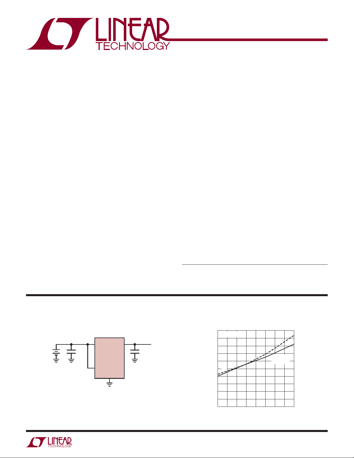
TYPICAL APPLICATION
3.3V, 20mA Supply with Shutdown
V
3.75V TO
20V
IN
1μF
IN
LT3009-3.3
SHDN
GND
OUT
1μF
V
OUT
3.3V
20mA
3009 TA01a
Dropout Voltage/Quiescent Current
500
I
= 20mA
LOAD
450 4.5
400
350 3.5
300
I
250
Q
200
150
DROPOUT VOLTAGE (mV)
100
50
0
–50 –25 0 25 50 75 100 125 150
TEMPERATURE (°C)
DROPOUT
VOLTAGE
5.0
QUIESCENT CURRENT (μA)
4.0
3.0
2.5
2.0
1.5
1.0
0.5
0
3009 TA01b
3009fc
1
Page 2

LT3009 Series
ABSOLUTE MAXIMUM RATINGS
(Note 1)
IN Pin Voltage .........................................................±22V
OUT Pin Voltage ......................................................±22V
Input-to-Output Differential Voltage ........................±22V
ADJ Pin Voltage ......................................................±22V
SHDN Pin Voltage (Note 8) .....................................±22V
Output Short-Circuit Duration .......................... Indefi nite
PIN CONFIGURATION
TOP VIEW
6
ADJ/NC*
T
EXPOSED PAD (PIN 7) IS GND, MUST BE SOLDERED TO PCB
* The ADJ pin is not connected in fi xed output voltage versions.
** See the Applications Information section.
1
2
3
DC PACKAGE
7
OUT
OUT
6-LEAD (2mm s 2mm) PLASTIC DFN
= 125°C, θJA = 65°C/W TO 85°C/W**
JMAX
GND
5
SHDN
IN
4
Operating Junction Temperature Range (Notes 2, 3)
(E, I Grades) ......................................–40°C to 125°C
Storage Temperature Range ...................–65°C to 150°C
Lead Temperature: Soldering, 10 sec
SC8 Package Only ............................................. 300°C
TOP VIEW
SHDN 1
GND 2
GND 3
GND 4
SC8 PACKAGE
8-LEAD PLASTIC SC70
T
= 125°C, θJA = 75°C/W TO 95°C/W**
JMAX
8 NC
7 ADJ/NC*
6 OUT
5 IN
ORDER INFORMATION
LEAD FREE FINISH TAPE AND REEL PART MARKING* PACKAGE DESCRIPTION TEMPERATURE RANGE
LT3009EDC#PBF LT3009EDC#TRPBF LCQX
LT3009IDC#PBF LT3009IDC#TRPBF LCQX
LT3009EDC-1.2#PBF LT3009EDC-1.2#TRPBF LDTW
LT3009IDC-1.2#PBF LT3009IDC-1.2#TRPBF LDTW
LT3009EDC-1.5#PBF LT3009EDC-1.5#TRPBF LDVB
LT3009IDC-1.5#PBF LT3009IDC-1.5#TRPBF LDVB
LT3009EDC-1.8#PBF LT3009EDC-1.8#TRPBF LDKC
LT3009IDC-1.8#PBF LT3009IDC-1.8#TRPBF LDKC
LT3009EDC-2.5#PBF LT3009EDC-2.5#TRPBF LDTY
LT3009IDC-2.5#PBF LT3009IDC-2.5#TRPBF LDTY
LT3009EDC-3.3#PBF LT3009EDC-3.3#TRPBF LDKD
LT3009IDC-3.3#PBF LT3009IDC-3.3#TRPBF LDKD
LT3009EDC-5#PBF LT3009EDC-5#TRPBF LDKF
LT3009IDC-5#PBF LT3009IDC-5#TRPBF LDKF
6-Lead (2mm × 2mm) Plastic DFN
6-Lead (2mm × 2mm) Plastic DFN
6-Lead (2mm × 2mm) Plastic DFN
6-Lead (2mm × 2mm) Plastic DFN
6-Lead (2mm × 2mm) Plastic DFN
6-Lead (2mm × 2mm) Plastic DFN
6-Lead (2mm × 2mm) Plastic DFN
6-Lead (2mm × 2mm) Plastic DFN
6-Lead (2mm × 2mm) Plastic DFN
6-Lead (2mm × 2mm) Plastic DFN
6-Lead (2mm × 2mm) Plastic DFN
6-Lead (2mm × 2mm) Plastic DFN
6-Lead (2mm × 2mm) Plastic DFN
6-Lead (2mm × 2mm) Plastic DFN
–40°C to 125°C
–40°C to 125°C
–40°C to 125°C
–40°C to 125°C
–40°C to 125°C
–40°C to 125°C
–40°C to 125°C
–40°C to 125°C
–40°C to 125°C
–40°C to 125°C
–40°C to 125°C
–40°C to 125°C
–40°C to 125°C
–40°C to 125°C
3009fc
2
Page 3

LT3009 Series
ORDER INFORMATION
LEAD FREE FINISH TAPE AND REEL PART MARKING* PACKAGE DESCRIPTION TEMPERATURE RANGE
LT3009ESC8#PBF LT3009ESC8#TRPBF LCQY 8-Lead Plastic SC70 –40°C to 125°C
LT3009ESC8-1.2#PBF LT3009ESC8-1.2#TRPBF LDTX 8-Lead Plastic SC70 –40°C to 125°C
LT3009ESC8-1.5#PBF LT3009ESC8-1.5#TRPBF LDVC 8-Lead Plastic SC70 –40°C to 125°C
LT3009ESC8-1.8#PBF LT3009ESC8-1.8#TRPBF LDKG 8-Lead Plastic SC70 –40°C to 125°C
LT3009ESC8-2.5#PBF LT3009ESC8-2.5#TRPBF LDTZ 8-Lead Plastic SC70 –40°C to 125°C
LT3009ESC8-3.3#PBF LT3009ESC8-3.3#TRPBF LDKH 8-Lead Plastic SC70 –40°C to 125°C
LT3009ESC8-5#PBF LT3009ESC8-5#TRPBF LDKJ 8-Lead Plastic SC70 –40°C to 125°C
LEAD BASED FINISH TAPE AND REEL PART MARKING* PACKAGE DESCRIPTION TEMPERATURE RANGE
LT3009EDC LT3009EDC#TR LCQX
LT3009IDC LT3009IDC#TR LCQX
LT3009EDC-1.2 LT3009EDC-1.2#TR LDTW
LT3009IDC-1.2 LT3009IDC-1.2#TR LDTW
LT3009EDC-1.5 LT3009EDC-1.5#TR LDVB
LT3009IDC-1.5 LT3009IDC-1.5#TR LDVB
LT3009EDC-1.8 LT3009EDC-1.8#TR LDKC
LT3009IDC-1.8 LT3009IDC-1.8#TR LDKC
LT3009EDC-2.5 LT3009EDC-2.5#TR LDTY
LT3009IDC-2.5 LT3009IDC-2.5#TR LDTY
LT3009EDC-3.3 LT3009EDC-3.3#TR LDKD
LT3009IDC-3.3 LT3009IDC-3.3#TR LDKD
LT3009EDC-5 LT3009EDC-5#TR LDKF
LT3009IDC-5 LT3009IDC-5#TR LDKF
LT3009ESC8 LT3009ESC8#TR LCQY 8-Lead Plastic SC70 –40°C to 125°C
LT3009ESC8-1.2 LT3009ESC8-1.2#TR LDTX 8-Lead Plastic SC70 –40°C to 125°C
LT3009ESC8-1.5 LT3009ESC8-1.5#TR LDVC 8-Lead Plastic SC70 –40°C to 125°C
LT3009ESC8-1.8 LT3009ESC8-1.8#TR LDKG 8-Lead Plastic SC70 –40°C to 125°C
LT3009ESC8-2.5 LT3009ESC8-2.5#TR LDTZ 8-Lead Plastic SC70 –40°C to 125°C
LT3009ESC8-3.3 LT3009ESC8-3.3#TR LDKH 8-Lead Plastic SC70 –40°C to 125°C
LT3009ESC8-5 LT3009ESC8-5#TR LDKJ 8-Lead Plastic SC70 –40°C to 125°C
Consult LTC Marketing for parts specifi ed with wider operating temperature ranges. *The temperature grade is identifi ed by a label on the shipping container.
For more information on lead free part marking, go to: http://www.linear.com/leadfree/
For more information on tape and reel specifi
cations, go to: http://www.linear.com/tapeandreel/
6-Lead (2mm × 2mm) Plastic DFN
6-Lead (2mm × 2mm) Plastic DFN
6-Lead (2mm × 2mm) Plastic DFN
6-Lead (2mm × 2mm) Plastic DFN
6-Lead (2mm × 2mm) Plastic DFN
6-Lead (2mm × 2mm) Plastic DFN
6-Lead (2mm × 2mm) Plastic DFN
6-Lead (2mm × 2mm) Plastic DFN
6-Lead (2mm × 2mm) Plastic DFN
6-Lead (2mm × 2mm) Plastic DFN
6-Lead (2mm × 2mm) Plastic DFN
6-Lead (2mm × 2mm) Plastic DFN
6-Lead (2mm × 2mm) Plastic DFN
6-Lead (2mm × 2mm) Plastic DFN
–40°C to 125°C
–40°C to 125°C
–40°C to 125°C
–40°C to 125°C
–40°C to 125°C
–40°C to 125°C
–40°C to 125°C
–40°C to 125°C
–40°C to 125°C
–40°C to 125°C
–40°C to 125°C
–40°C to 125°C
–40°C to 125°C
–40°C to 125°C
3009fc
3
Page 4

LT3009 Series
ELECTRICAL CHARACTERISTICS
The l denotes the specifi cations which apply over the full operating
temperature range, otherwise specifi cations are at T
PARAMETER CONDITIONS MIN TYP MAX UNITS
Operating Voltage
Regulated Output Voltage (Note 4) LT3009-1.2: V
ADJ Pin Voltage (Notes 3, 4) VIN = 1.6V, I
Line Regulation (Note 3)
Load Regulation (Note 3) LT3009-1.2: V
Dropout Voltage
V
= V
IN
OUT(NOMINAL)
Quiescent Current (Notes 6, 7) I
GND Pin Current
VIN = V
OUT(NOMINAL)
(Notes 5, 6)
+ 0.5V (Notes 6, 7)
= 25°C. (Note 2)
J
= 1.7V, I
1.7V < V
IN
< 20V, 1μA < I
IN
LT3009-1.5: VIN = 2V, I
2V < V
< 20V, 1μA < I
IN
LT3009-1.8: VIN = 2.3V, I
2.3V < V
< 20V, 1μA < I
IN
LT3009-2.5: VIN = 3V, I
3V < V
< 20V, 1μA < I
IN
LT3009-3.3: V
3.8V < V
= 3.8V, I
IN
< 20V, 1μA < I
IN
LT3009-5: VIN = 5.5V, I
3.8V < V
1.6V < V
LT3009-1.2: ΔV
LT3009-1.5: ΔV
LT3009-1.8: ΔV
LT3009-2.5: ΔV
LT3009-3.3: ΔV
LT3009-5: ΔV
LT3009: ΔV
LT3009-1.5: V
LT3009-1.8: V
LT3009-2.5: V
LT3009-3.3: V
LT3009-5: V
LT3009: V
I
LOAD
I
LOAD
I
LOAD
I
LOAD
I
LOAD
I
LOAD
I
LOAD
I
LOAD
LOAD
I
LOAD
I
LOAD
I
LOAD
I
LOAD
I
LOAD
I
LOAD
< 20V, 1μA < I
IN
LOAD
< 20V, 1μA < I
IN
= 100μA
= 100μA
= 1mA
= 1mA
= 10mA
= 10mA
= 20mA
= 20mA
= 0μA
= 0μA
= 0μA
= 100μA
= 1mA
= 10mA
= 20mA
= 100μA
= 1.7V to 20V, I
IN
= 2.0V to 20V, I
IN
= 2.3V to 20V, I
IN
= 3.0V to 20V, I
IN
= 3.8V to 20V, I
IN
= 5.5V to 20V, I
IN
= 1.6V to 20V, I
IN
= 1.7V, I
IN
= 2V, I
IN
= 2.3V, I
IN
= 3V, I
IN
= 3.8V, I
IN
= 5.5V, I
IN
= 1.6V, I
IN
= 100μA
LOAD
< 20mA
LOAD
= 100μA
LOAD
< 20mA
LOAD
= 100μA
LOAD
< 20mA
LOAD
= 100μA
LOAD
< 20mA
LOAD
= 100μA
LOAD
< 20mA
LOAD
= 100μA
LOAD
< 20mA
LOAD
< 20mA
LOAD
= 1μA to 20mA
LOAD
= 1μA to 20mA
LOAD
= 1μA to 20mA
LOAD
= 1μA to 20mA
LOAD
= 1μA to 20mA
LOAD
= 1μA to 20mA
LOAD
= 1μA to 20mA
LOAD
LOAD
LOAD
LOAD
LOAD
LOAD
LOAD
LOAD
= 1mA
= 1mA
= 1mA
= 1mA
= 1mA
= 1mA
= 1mA
l
1.6 20 V
1.188
l
1.176
1.485
l
1.470
1.782
l
1.764
2.475
l
2.45
3.267
l
3.234
4.950
l
4.900
594
l
588
l
l
l
l
l
l
l
l
l
l
l
l
l
l
1.2
1.2
1.5
1.5
1.8
1.8
2.5
2.5
3.3
3.3
5
5
600
600
0.8
1.0
1.2
1.7
2.2
3.3
0.4
1.4
1.8
2.1
2.9
3.9
5.8
0.7
1.212
1.224
1.515
1.530
1.818
1.836
2.525
3.333
3.366
5.050
5.100
115 180
l
170 250
l
250 310
l
280 350
l
3
l
l
l
l
l
l
3
6
23
200
450
1000
2.55
606
612
3.0
3.8
4.5
6.3
8.3
12.5
1.5
6
7.5
9.0
12.5
16.5
25
3
250
350
410
450
6
6
12
50
500
mV
mV
mV
mV
mV
mV
mV
mV
mV
mV
mV
mV
mV
mV
mV
mV
mV
mV
mV
mV
mV
mV
mV
mV
μA
μA
μA
μA
μA
μA
μA
V
V
V
V
V
V
V
V
V
V
V
V
4
3009fc
Page 5
LT3009 Series
ELECTRICAL CHARACTERISTICS
The l denotes the specifi cations which apply over the full operating
temperature range, otherwise specifi cations are at T
PARAMETER CONDITIONS MIN TYP MAX UNITS
Output Voltage Noise (Note 9) C
ADJ Pin Bias Current
Shutdown Threshold V
SHDN Pin Current V
Quiescent Current in Shutdown V
Ripple Rejection (Note 3) V
Current Limit V
Input Reverse Leakage Current V
Reverse Output Current V
Note 1: Stresses beyond those listed under Absolute Maximum Ratings
may cause permanent damage to the device. Exposure to any Absolute
Maximum Rating condition for extended periods may affect device
reliability and lifetime.
Note 2: The LT3009 regulators are tested and specifi ed under pulse load
conditions such that T
Performance at –40°C and 125°C is assured by design, characterization
and correlation with statistical process controls. The LT3009I is guaranteed
over the full –40°C to 125°C operating junction temperature range.
Note 3: The LT3009 adjustable version is tested and specifi ed for these
conditions with the ADJ pin connected to the OUT pin.
Note 4: Operating conditions are limited by maximum junction temperature.
The regulated output voltage specifi cation will not apply for all possible
combinations of input voltage and output current. When operating at the
maximum input voltage, the output current range must be limited. When
operating at the maximum output current, the input voltage must be limited.
Note 5: Dropout voltage is the minimum input to output voltage differential
needed to maintain regulation at a specifi ed output current. In dropout,
the output voltage equals (V
≈ TA. The LT3009E is 100% tested at TA = 25°C.
J
– V
IN
). For the LT3009-1.2, dropout
DROPOUT
= 25°C. (Note 2)
J
= 1μF, I
OUT
= Off to On
OUT
V
= On to Off
OUT
= 0V, VIN = 20V
SHDN
V
= 20V, VIN = 20V
SHDN
= 6V, V
IN
– V
IN
OUT
f
= 120Hz, I
RIPPLE
LT3009
LT3009-1.2
LT3009-1.5
LT3009-1.8
LT3009-2.5
LT3009-3.3
LT3009-5
= 20V, V
IN
V
= V
IN
OUT(NOMINAL)
= –20V, V
IN
= 1.2V, VIN = 0 0.6 10 μA
OUT
= 20mA, BW = 10Hz to 100kHz 150 μV
LOAD
l
–10 0.3 10 nA
= 0V
SHDN
= 1.5V, V
LOAD
= 0
OUT
= 0
OUT
= 0.5V
RIPPLE
= 20mA
+ 1V, ΔV
OUT
,
P-P
= –5%
l
l
0.2
l
l
l
60
57
55.5
54
52
49
44
l
22
l
0.66
0.36
0.5
72
68
67
66
63
61
56
60 mA
200 350 μA
1.5 V
±1
1.6
<1 μA
voltage will be limited by the minimum input voltage under some voltage/
load conditions.
Note 6: To satisfy minimum input voltage requirements, the LT3009
adjustable version is tested and specifi ed for these conditions with an
external resistor divider (61.9k bottom, 280k top) which sets V
OUT
The external resistor divider adds 9.69μA of DC load on the output. This
external current is not factored into GND pin current.
Note 7: GND pin current is tested with V
= V
IN
OUT(NOMINAL)
+ 0.5V and a
current source load. GND pin current will increase in dropout. For the fi xed
output voltage versions, an internal resistor divider will add to the GND
pin current (∼2μA for the LT3009-5, ∼ 1μA for the LT3009-1.2, LT3009-1.5,
LT3009-1.8, LT3009-2.5 and LT3009-3.3). See the GND Pin Current curves
in the Typical Performance Characteristics section.
Note 8: The SHDN pin can be driven below GND only when tied to the IN
pin directly or through a pull-up resistor. If the SHDN pin is driven below
GND by more than –0.3V while IN is powered, the output will turn on.
Note 9: Output noise is listed for the adjustable version with the ADJ pin
connected to the OUT pin. See the RMS Output Noise vs Load Current
curve in the Typical Performance Characteristics Section.
RMS
μA
μA
dB
dB
dB
dB
dB
dB
dB
mA
to 3.3V.
V
3009fc
5
Page 6
LT3009 Series
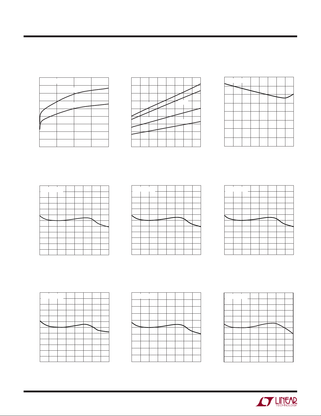
TYPICAL PERFORMANCE CHARACTERISTICS
Dropout Voltage Dropout Voltage Minimum Input Voltage
450
I
= 20mA
LOAD
400
350
300
250
200
150
DROPOUT VOLTAGE (mV)
100
50
0
0
TA = 125°C
TA = 25°C
515
OUTPUT CURRENT (mA)
10
ADJ Pin Voltage
0.612
I
= 100μA
LOAD
0.610
0.608
0.606
0.604
0.602
0.600
0.598
0.596
ADJ PIN VOLTAGE (V)
0.594
0.592
0.590
0.588
–50 –25 0 25 50 75 100 125 150
TEMPERATURE (°C)
20
3009 G01
3009 G04
450
400
350
300
250
200
150
DROPOUT VOLTAGE (mV)
100
50
0
20mA
1mA
–50 –25 0 25 50 75 100 125 150
TEMPERATURE (°C)
10mA
100μA
Output Voltage
LT3009-1.2
1.224
I
= 100μA
LOAD
1.220
1.216
1.212
1.208
1.204
1.200
1.196
1.192
OUTPUT VOLTAGE (V)
1.188
1.184
1.180
1.176
–50 –25 0 25 50 75 100 125 150
TEMPERATURE (°C)
TA = 25°C, unless otherwise noted.
1.6
I
= 20mA
LOAD
1.4
1.2
1
0.8
0.6
0.4
MINIMUM INPUT VOLTAGE (V)
0.2
0
–50 –25 0 25 50 75 100 125 150
3009 G02
TEMPERATURE (°C)
Output Voltage
LT3009-1.5
1.530
I
= 100μA
LOAD
1.525
1.520
1.515
1.510
1.505
1.500
1.495
1.490
OUTPUT VOLTAGE (V)
1.485
1.480
1.475
1.470
–50 –25 0 25 50 75 100 125 150
3009 G27
TEMPERATURE (°C)
3009 G03
3009 G28
Output Voltage
LT3009-1.8
1.836
I
= 100μA
LOAD
1.830
1.824
1.818
1.812
1.806
1.800
1.794
1.788
OUTPUT VOLTAGE (V)
1.782
1.776
1.770
1.764
–50 –25 0 25 50 75 100 125 150
TEMPERATURE (°C)
6
3009 G05
Output Voltage
LT3009-2.5
2.55
I
= 100μA
LOAD
2.54
2.53
2.52
2.51
2.50
2.49
2.48
OUTPUT VOLTAGE (V)
2.47
2.46
2.45
–50 –25 0 25 50 75 100 125 150
TEMPERATURE (°C)
3009 G29
Output Voltage
LT3009-3.3
3.366
I
= 100μA
LOAD
3.355
3.344
3.333
3.322
3.311
3.300
3.289
3.278
OUTPUT VOLTAGE (V)
3.267
3.256
3.245
3.234
–50 –25 0 25 50 75 100 125 150
TEMPERATURE (°C)
3009 G06
3009fc
Page 7

LT3009 Series
TYPICAL PERFORMANCE CHARACTERISTICS
Output Voltage
LT3009-5
5.100
I
= 100μA
LOAD
5.075
5.050
5.025
5.000
4.975
OUTPUT VOLTAGE (V)
4.950
4.925
4.900
–50 –25 0 25 50 75 100 125 150
TEMPERATURE (°C)
3009 G07
Quiescent Current Quiescent Current
20
18
16
14
12
10
8
6
QUIESCENT CURRENT (μA)
4
2
0
0
2
1
3
INPUT VOLTAGE (V)
4
5
6
LT3009-1.2
LT3009-1.5
LT3009-1.8
8
7
9
3009 G10
10
ADJ Pin Bias Current
10
8
6
4
2
0
–2
–4
ADJ PIN BIAS CURRENT (nA)
–6
–8
–10
–50 –25 0 25 50 75 100 125 150
TEMPERATURE (°C)
20
18
16
14
12
10
8
6
QUIESCENT CURRENT (μA)
4
2
0
0
2
1
3
INPUT VOLTAGE (V)
4
5
6
LT3009-2.5
LT3009-3.3
LT3009-5
7
TA = 25°C, unless otherwise noted.
Adjustable Version
Quiescent Current
6
5
4
3
2
QUIESCENT CURRENT (μA)
1
0
–50 –25 0 25 50 75 100 125 150
3009 G08
TEMPERATURE (°C)
GND Pin Current
LT3009-1.2
500
450
400
350
300
250
200
150
GND PIN CURRENT (μA)
100
10
9
8
3009 G30
50
0
0
RL = 12k, IL = 100μA
3
2
1
INPUT VOLTAGE (V)
RL = 60Ω, IL = 20mA
RL = 120Ω, IL = 10mA
RL = 1.2k, IL = 1mA
4
6
5
7
3009 G09
10
9
8
3009 G31
3009fc
7
Page 8

LT3009 Series
TYPICAL PERFORMANCE CHARACTERISTICS
GND Pin Current
LT3009-1.5
500
450
400
350
300
250
200
150
GND PIN CURRENT (μA)
100
50
0
0
1
RL = 15k, IL = 100μA
3
2
INPUT VOLTAGE (V)
GND Pin Current
LT3009-3.3
500
450
400
350
300
250
200
150
GND PIN CURRENT (μA)
100
50
0
RL = 33k, IL = 100μA
1
3
INPUT VOLTAGE (V)
02
RL = 75Ω, IL = 20mA
RL = 150Ω, IL = 10mA
RL = 1.5k, IL = 1mA
4
6
5
7
RL = 165Ω, IL = 20mA
RL = 330Ω, IL = 10mA
RL = 3.3k, IL = 1mA
4
6
5
7
10
9
8
3009 G32
10
9
8
3009 G12
GND Pin Current
LT3009-1.8
500
450
400
350
300
250
200
150
GND PIN CURRENT (μA)
100
50
0
0
RL = 18k, IL = 100μA
3
2
1
INPUT VOLTAGE (V)
GND Pin Current
LT3009-5
450
400
350
300
250
200
150
GND PIN CURRENT (μA)
100
50
0
0
RL = 50k, IL = 100μA
3
2
1
INPUT VOLTAGE (V)
RL = 90Ω, IL = 20mA
RL = 180Ω, IL = 10mA
RL = 1.8k, IL = 1mA
4
6
5
7
RL = 250Ω, IL = 20mA
RL = 500Ω, IL = 10mA
RL = 5k, IL = 1mA
4
6
5
7
TA = 25°C, unless otherwise noted.
GND Pin Current
LT3009-2.5
500
450
400
350
300
250
200
150
GND PIN CURRENT (μA)
100
10
9
8
3009 G11
50
0
0
RL = 25k, IL = 100μA
3
2
1
INPUT VOLTAGE (V)
GND Pin Current vs I
1000
VIN = 3.8V
= 3.3V
V
OUT
100
10
GND CURRENT (μA)
10
9
8
3009 G13
1
0.001
0.01 0.1 1 10
RL = 125Ω, IL = 20mA
RL = 250Ω, IL = 10mA
RL = 2.5k, IL = 1mA
4
6
5
7
LOAD
LOAD (mA)
10
9
8
3009 G33
100
3009 G14
8
3009fc
Page 9

LT3009 Series
TYPICAL PERFORMANCE CHARACTERISTICS
SHDN Pin Thresholds
1.4
1.2
1.0
0.8
0.6
0.4
0.2
SHDN PIN THRESHOLD VOLTAGE (V)
0
–50 –25 0 25 50 75 100 125 150
OFF TO ON
ON TO OFF
TEMPERATURE (°C)
Current Limit
70
60
50
40
30
20
CURRENT LIMIT (mA)
10
0
–50 –25 0 25 50 75 100 125 150
VIN = 20V
VIN = 1.6V
TEMPERATURE (°C)
3009 G15
3009 G18
SHDN Pin Input Current SHDN Pin Input Current
500
450
400
350
300
250
200
150
100
SHDN PIN INPUT CURRENT (nA)
50
0
4 8 12 16 2020 6 10 14 18
SHDN PIN VOLTAGE (V)
Reverse Output Current
50
OUT = ADJ = 1.2V
45
IN = SHDN = GND
40
35
30
25
20
15
10
REVERSE OUTPUT CURRENT (μA)
5
0
–50 –25 0 25 50 75 100 125 150
ADJ
TEMPERATURE (°C)
TA = 25°C, unless otherwise noted.
1600
V
= 20V
SHDN
1400
1200
1000
800
600
400
SHDN PIN INPUT CURRENT (nA)
200
0
–50 –25 0 25 50 75 100 125 150
3009 G16
TEMPERATURE (°C)
Input Ripple Rejection
OUT
3009 G19
90
80
70
60
50
40
30
20
INPUT RIPPLE REJECTION (dB)
10
0
10 100 1k 10k 100k 1M
VIN = 2V + 50mV
V
I
FREQUENCY (Hz)
OUT
LOAD
= 600mV
= 20mA
4.7μF
1μF
3009 G17
RMS
3009 G20
3009fc
9
Page 10

LT3009 Series
TYPICAL PERFORMANCE CHARACTERISTICS
Input Ripple Rejection
80
70
60
50
40
30
20
INPUT RIPPLE REJECTION (dB)
VIN = V
10
RIPPLE AT f = 120Hz
I
0
–50 –25 0 25 50 75 100 125 150
(NOMINAL) + 1V + 0.5V
OUT
= 20mA
LOAD
P-P
TEMPERATURE (°C)
3009 G21
RMS Output Noise vs Load
Current (10Hz to 100kHz) Transient ResponseTransient Response
700
600
)
500
RMS
400
300
200
OUTPUT NOISE (μV
100
5V
3.3V
2.5V
1.8V
1.5V
1.2V
600mV
Load Regulation Output Noise Spectral Density
3.0
2.5
2.0
1.5
1.0
0.5
0
LOAD REGULATION (mV)
–0.5
–1.0
–50 –25 0 25 50 75 100 125 150
TEMPERATURE (°C)
I
= 1mA TO 20mA
OUT
= 5.5V
V
IN
= 5V
V
OUT
= 1μF
C
OUT
V
OUT
50mV/DIV
I
OUT
20mA/DIV
ΔIL = 1μA TO 20mA
= 600mV
V
OUT
= 1.6V
V
IN
500μs/DIV
TA = 25°C, unless otherwise noted.
100
10
1
OUTPUT NOISE SPECTRAL DENSITY (μV√Hz)
0.1
10 100 1k 10k 100k
I
= 1mA TO 20mA
OUT
= 5.5V
V
IN
= 5V
V
OUT
= 4.7μF
C
OUT
FREQUENCY (Hz)
500μs/DIV
3009 G22
3009 G25
V
OUT
50mV/DIV
I
OUT
20mA/DIV
5V
3.3V
2.5V
1.8V
1.5V
1.2V
1V
0.6V
3009 G23
3009 G26
0
0.001
10
0.01 0.1 1 100
I
(mA)
LOAD
10
3009 G24
3009fc
Page 11

LT3009 Series
PIN FUNCTIONS
SHDN (Pin 1/Pin 5): Shutdown. Pulling the SHDN pin
low puts the LT3009 into a low power state and turns the
output off. If unused, tie the SHDN pin to V
does not function if the SHDN pin is not connected. The
SHDN pin cannot be driven below GND unless tied to the
IN pin. If the SHDN pin is driven below GND while IN is
powered, the output will turn on. SHDN pin logic cannot
be referenced to a negative rail.
GND (Pins 2, 3, 4/Pin 6): Ground. Connect the bottom
of the resistor divider that sets output voltage directly to
GND for the best regulation.
IN (Pin 5/Pin 4): Input. The IN pin supplies power to the
device. The LT3009 requires a bypass capacitor at IN if
the device is more than six inches away from the main
input fi lter capacitor. In general, the output impedance
of a battery rises with frequency, so it is advisable to
include a bypass capacitor in battery-powered circuits. A
bypass capacitor in the range of 0.1μF to 10μF will suffi ce. The LT3009 withstands reverse voltages on the IN
pin with respect to ground and the OUT pin. In the case
of a reversed input, which occurs with a battery plugged
in backwards, the LT3009 acts as if a large resistor is in
series with its input. Limited reverse current fl ows into
the LT3009 and no reverse voltage appears at the load.
The device protects both itself and the load.
(SC70/DFN)
. The LT3009
IN
OUT (Pin 6/Pins 2, 3): Output. This pin supplies power to
the load. Use a minimum output capacitor of 1μF to prevent
oscillations. Large load transient applications require larger
output capacitors to limit peak voltage transients. See the
Applications Information section for more information on
output capacitance and reverse output characteristics.
ADJ (Pin 7/Pin 1): Adjust. This pin is the error amplifi er’s
inverting terminal. Its 300pA typical input bias current
fl ows out of the pin (see curve of ADJ Pin Bias Current vs
Temperature in the Typical Performance Characteristics
section). The ADJ pin voltage is 600mV referenced to GND
and the output voltage range is 600mV to 19.5V. This pin
is not connected in the fi xed output voltage versions.
NC (Pins 7, 8/Pin 1): No Connect. For the adjustable voltage
version, Pin 8 is an NC pin in the SC70 package. For the
fi xed voltage versions, Pin 7 and Pin 8 are NC pins in the
SC70 package, and Pin 1 is an NC pin in the DFN package.
NC pins are not tied to any internal circuitry. They may be
fl oated, tied to V
Exposed Pad (Pin 7, DFN Package Only): Ground. The
Exposed Pad (backside) of the DFN package is an electrical connection to GND. To ensure optimum performance,
solder Pin 7 to the PCB and tie directly to Pin 6.
or tied to GND.
IN
3009fc
11
Page 12

LT3009 Series
T
APPLICATIONS INFORMATION
The LT3009 is a low dropout linear regulator with ultralow quiescent current and shutdown. Quiescent current is
extremely low at 3μA and drops well below 1μA in shutdown. The device supplies up to 20mA of output current.
Dropout voltage at 20mA is typically 280mV. The LT3009
incorporates several protection features, making it ideal for
use in battery-powered systems. The device protects itself
against both reverse-input and reverse-output voltages.
In battery backup applications, where a backup battery
holds up the output when the input is pulled to ground,
the LT3009 acts as if a blocking diode is in series with its
output and prevents reverse current fl ow. In applications
where the regulator load returns to a negative supply, the
output can be pulled below ground by as much as 22V
without affecting startup or normal operation.
Adjustable Operation
The LT3009 has an output voltage range of 0.6V to 19.5V.
Figure 1 shows that output voltage is set by the ratio of two
external resistors. The IC regulates the output to maintain
the ADJ pin voltage at 600mV referenced to ground. The
current in R1 equals 600mV/R1 and the current in R2 is
the current in R1 minus the ADJ pin bias current. The
ADJ pin bias current, typically 300pA at 25°C, fl ows out
of the pin. Calculate the output voltage using the formula
in Figure 1. An R1 value of 619k sets the divider current
to 0.97μA. Do not make R1’s value any greater than 619k
to minimize output voltage errors due to the ADJ pin bias
current and to insure stability under minimum load conditions. In shutdown, the output turns off and the divider
current is zero. Curves of ADJ Pin Voltage vs Temperature
and ADJ Pin Bias Current vs Temperature appear in the
Typical Performance Characteristics.
Specifi cations for output voltages greater than 0.6V are
proportional to the ratio of the desired output voltage to
0.6V: V
/0.6V. For example, load regulation for an output
OUT
current change of 100μA to 20mA is –0.7mV typical at
= 0.6V. At V
V
OUT
5
06
.
V
07 583
•( . ) .− = −
V
= 5V, load regulation is:
OUT
mV mV
Table 1 shows resistor divider values for some common output voltages with a resistor divider current of
about 1μA.
Table 1. Output Voltage Resistor Divider Values
V
OUT
1V 604k 402k
1.2V 604k 604k
1.5V 590k 887k
1.8V 590k 1.18M
2.5V 590k 1.87M
3V 590k 2.37M
3.3V 619k 2.8M
5V 590k 4.32M
R1 R2
Because the ADJ pin is relatively high impedance (depending on the resistor divider used), stray capacitances
at this pin should be minimized. Special attention should
be given to any stray capacitances that can couple external signals onto the ADJ pin producing undesirable
output transients or ripple.
Extra care should be taken in assembly when using high
valued resistors. Small amounts of board contamination
can lead to signifi cant shifts in output voltage. Appropriate post-assembly board cleaning measures should
12
V
= 600mV* (1 + R2/R1) – (I
OUT
= 600mV
V
ADJ
= 0.3nA at 25°C
I
ADJ
OUTPUT RANGE = 0.6V to 19.5V
• R2)
ADJ
Figure 1. Adjustable Operation
V
IN
IN
LT3009
SHDN
GND
OUT
ADJ
V
OU
R2
R1
3009fc
Page 13

APPLICATIONS INFORMATION
LT3009 Series
be implemented to prevent board contamination. If the
board is to be subjected to humidity cycling or if board
cleaning measures cannot be guaranteed, consideration
should be given to using resistors an order of magnitude
smaller than in Table 1 to prevent contamination from
causing unwanted shifts in the output voltage.
Output Capacitance and Transient Response
The LT3009 is stable with a wide range of output capacitors. The ESR of the output capacitor affects stability, most
notably with small capacitors. Use a minimum output
capacitor of 1μF with an ESR of 3Ω or less to prevent oscillations. The LT3009 is a micropower device and output
load transient response is a function of output capacitance.
Larger values of output capacitance decrease the peak
deviations and provide improved transient response for
larger load current changes.
Give extra consideration to the use of ceramic capacitors.
Manufacturers make ceramic capacitors with a variety of
dielectrics, each with different behavior across temperature and applied voltage. The most common dielectrics
are specifi ed with EIA temperature characteristic codes
of Z5U, Y5V, X5R and X7R. The Z5U and Y5V dielectrics
provide high C-V products in a small package at low cost,
but exhibit strong voltage and temperature coeffi cients as
shown in Figures 2 and 3. When used with a 5V regulator,
a 16V 10μF Y5V capacitor can exhibit an effective value
as low as 1μF to 2μF for the DC bias voltage applied and
over the operating temperature range. The X5R and X7R
dielectrics yield more stable characteristics and are more
suitable for use as the output capacitor. The X7R type has
better stability across temperature, while the X5R is less
expensive and is available in higher values. One must still
exercise care when using X5R and X7R capacitors; the
X5R and X7R codes only specify operating temperature
range and maximum capacitance change over temperature.
Capacitance change due to DC bias with X5R and X7R
capacitors is better than Y5V and Z5U capacitors, but can
still be signifi cant enough to drop capacitor values below
appropriate levels. Capacitor DC bias characteristics tend
to improve as component case size increases, but expected
capacitance at operating voltage should be verifi ed.
20
0
–20
–40
–60
CHANGE IN VALUE (%)
–80
–100
0
BOTH CAPACITORS ARE 16V,
1210 CASE SIZE, 10μF
X5R
Y5V
26
4
8
DC BIAS VOLTAGE (V)
14
12
10
16
3009 F02
40
20
0
–20
–40
–60
CHANGE IN VALUE (%)
–80
BOTH CAPACITORS ARE 16V,
1210 CASE SIZE, 10μF
–100
–50
–25 0
Y5V
50 100 125
25 75
TEMPERATURE (°C)
X5R
3009 F03
Figure 2. Ceramic Capacitor DC Bias Characteristics Figure 3. Ceramic Capacitor Temperature Characteristics
3009fc
13
Page 14

LT3009 Series
4
APPLICATIONS INFORMATION
Voltage and temperature coeffi cients are not the only
sources of problems. Some ceramic capacitors have a
piezoelectric response. A piezoelectric device generates
voltage across its terminals due to mechanical stress,
similar to the way a piezoelectric accelerometer or microphone works. For a ceramic capacitor, the stress can be
induced by vibrations in the system or thermal transients.
The resulting voltages produced can cause appreciable
amounts of noise, especially when a ceramic capacitor is
used for noise bypassing. A ceramic capacitor produced
Figure 4’s trace in response to light tapping from a pencil.
Similar vibration induced behavior can masquerade as
increased output voltage noise.
V
= 0.6V
OUT
= 22μF
C
OUT
= 10μA
I
LOAD
V
OUT
500μV/DIV
100ms/DIV
Figure 4. Noise Resulting from Tapping
on a Ceramic Capacitor
3009 F0
Thermal Considerations
The LT3009’s maximum rated junction temperature of
125°C limits its power-handling capability. Two components
comprise the power dissipated by the device:
1. Output current multiplied by the input/output voltage
differential: I
• (VIN – V
OUT
OUT
)
2. GND pin current multiplied by the input voltage:
• V
I
GND
IN
GND pin current is found by examining the GND Pin Current curves in the Typical Performance Characteristics
section. Power dissipation equals the sum of the two
components listed prior.
The LT3009 regulator has internal thermal limiting designed
to protect the device during overload conditions. For continuous normal conditions, do not exceed the maximum
junction temperature rating of 125°C. Carefully consider
all sources of thermal resistance from junction to ambient including other heat sources mounted in proximity to
the LT3009. For surface mount devices, heat sinking is
accomplished by using the heat spreading capabilities of
the PC board and its copper traces. Copper board stiffeners
and plated through-holes can also be used to spread the
heat generated by power devices.
14
3009fc
Page 15

APPLICATIONS INFORMATION
LT3009 Series
The following tables list thermal resistance for several different board sizes and copper areas. All measurements
were taken in still air on 3/32" FR-4 board with one ounce
copper.
Table 2: Measured Thermal Resistance for DC Package
COPPER AREA
2
2500mm
1000mm
225mm
100mm
50mm
*Device is mounted on the topside.
2500mm
2
2500mm
2
2500mm
2
2500mm
2
2500mm
Table 3: Measured Thermal Resistance for SC70 Package
COPPER AREA
2
2500mm
1000mm
225mm
100mm
50mm
*Device is mounted on the topside.
2500mm
2
2500mm
2
2500mm
2
2500mm
2
2500mm
2
2
2
2
2
2
2
2
2
2
BOARD
AREA
2500mm
2500mm
2500mm
2500mm
2500mm
BOARD
AREA
2500mm
2500mm
2500mm
2500mm
2500mm
THERMAL RESISTANCE
(JUNCTION-TO-AMBIENT)TOPSIDE* BACKSIDE
2
2
2
2
2
(JUNCTION-TO-AMBIENT)TOPSIDE* BACKSIDE
2
2
2
2
2
65°C/W
70°C/W
75°C/W
80°C/W
85°C/W
THERMAL RESISTANCE
75°C/W
80°C/W
85°C/W
90°C/W
95°C/W
Calculating Junction Temperature
Example: Given an output voltage of 3.3V, an input voltage range of 12V ±5%, an output current range of 0mA
to 20mA and a maximum ambient temperature of 85°C,
what will the maximum junction temperature be for an
application using the DC package?
The power dissipated by the device is equal to:
I
OUT(MAX)
(V
IN(MAX)
– V
OUT
) + I
GND
(V
IN(MAX)
)
where,
at (I
= 20mA
= 12.6V
= 20mA, VIN = 12.6V) = 0.45mA
OUT
I
OUT(MAX)
V
IN(MAX)
I
GND
So,
P = 20mA(12.6V – 3.3V) + 0.45mA(12.6V) = 191.7mW
The thermal resistance will be in the range of 65°C/W to
85°C/W depending on the copper area. So the junction
temperature rise above ambient will be approximately
equal to:
0.1917W(75°C/W) = 14.4°C
The maximum junction temperature equals the maximum
junction temperature rise above ambient plus the maximum
ambient temperature or:
T
J(MAX)
= 85°C + 14.4°C = 99.4°C
3009fc
15
Page 16

LT3009 Series
APPLICATIONS INFORMATION
Protection Features
The LT3009 incorporates several protection features that
make it ideal for use in battery-powered circuits. In addition to the normal protection features associated with
monolithic regulators, such as current limiting and thermal
limiting, the device also protects against reverse-input
voltages, reverse-output voltages and reverse output-toinput voltages.
Current limit protection and thermal overload protection
protect the device against current overload conditions at
the output of the device. For normal operation, do not
exceed a junction temperature of 125°C.
The LT3009 IN pin withstands reverse voltages of 22V. The
device limits current fl ow to less than 1mA (typically less
than 220μA) and no negative voltage appears at OUT. The
device protects both itself and the load against batteries
that are plugged in backwards.
The SHDN pin cannot be driven below GND unless tied to
the IN pin. If the SHDN pin is driven below GND while IN
is powered, the output will turn on. SHDN pin logic cannot
be referenced to a negative rail.
The LT3009 incurs no damage if OUT is pulled below
ground. If IN is left open circuit or grounded, OUT can be
pulled below ground by 22V. No current fl ows from the
pass transistor connected to OUT. However, current fl ows
in (but is limited by) the resistor divider that sets output
voltage. Current fl ows from the bottom resistor in the
divider and from the ADJ pin’s internal clamp through the
top resistor in the divider to the external circuitry pulling
OUT below ground. If IN is powered by a voltage source,
OUT sources current equal to its current limit capability
and the LT3009 protects itself by thermal limiting if necessary. In this case, grounding the SHDN pin turns off the
LT3009 and stops OUT from sourcing current.
The LT3009 incurs no damage if the ADJ pin is pulled
above or below ground by 22V. If IN is left open circuit or
grounded, ADJ acts like a 100k resistor in series with a
diode when pulled above or below ground.
In circuits where a backup battery is required, several
different input/output conditions can occur. The output
voltage may be held up while the input is either pulled
to ground, pulled to some intermediate voltage or is left
open circuit. Current fl ow back into the output follows the
curve shown in Figure 5.
If the LT3009 IN pin is forced below the OUT pin or the
OUT pin is pulled above the IN pin, input current typically
drops to less than 1μA. This occurs if the LT3009 input is
connected to a discharged (low voltage) battery and either
a backup battery or a second regulator circuit holds up
the output. The state of the SHDN pin has no effect in the
reverse current if OUT is pulled above IN.
16
100
90
80
70
60
50
40
30
REVERSE CURRENT (μA)
20
10
0
21
0
OUTPUT AND ADJ VOLTAGE (V)
Figure 5. Reverse Output Current
ADJ CURRENT
OUT CURRENT
67 9
43
5
8
10
3009 F05
3009fc
Page 17

TYPICAL APPLICATIONS
V
IN
12V
1μF 1μF
NO PROTECTION
DIODES NEEDED!
IN
SHDN
OUT
LT3009-3.3
GND
LT3009 Series
Keep-Alive Power Supply
3.3V
LOAD:
SYSTEM MONITOR,
VOLATILE MEMORY, ETC.
3009 TA02
Last-Gasp Circuit
V
LINE
12V TO 15V
D
CHARGE
R
LIMIT
LINE POWER
IN
1μFSUPERCAP 1μF
SHDN
OUT
LT3009-5
GND
5V
SENSE
LINE
INTERRUPT
DETECT
PWR
GND
FAULT
3009 TA03
TO
MONITORING
CENTER
3009fc
17
Page 18

LT3009 Series
PACKAGE DESCRIPTION
DC Package
6-Lead Plastic DFN (2mm × 2mm)
(Reference LTC DWG # 05-08-1703)
2.50 p0.05
1.15 p0.05
0.675 p0.05
0.61 p0.05
(2 SIDES)
0.50 BSC
1.42 p0.05
(2 SIDES)
RECOMMENDED SOLDER PAD PITCH AND DIMENSIONS
NOTE:
1. DRAWING TO BE MADE A JEDEC PACKAGE OUTLINE M0-229 VARIATION OF (WCCD-2)
2. DRAWING NOT TO SCALE
3. ALL DIMENSIONS ARE IN MILLIMETERS
4. DIMENSIONS OF EXPOSED PAD ON BOTTOM OF PACKAGE DO NOT INCLUDE
MOLD FLASH. MOLD FLASH, IF PRESENT, SHALL NOT EXCEED 0.15mm ON ANY SIDE
5. EXPOSED PAD SHALL BE SOLDER PLATED
6. SHADED AREA IS ONLY A REFERENCE FOR PIN 1 LOCATION ON THE
TOP AND BOTTOM OF PACKAGE
PACKAGE
OUTLINE
0.25 p 0.05
PIN 1 BAR
TOP MARK
(SEE NOTE 6)
0.200 REF
2.00 p0.10
(4 SIDES)
0.75 p0.05
0.00 – 0.05
R = 0.115
TYP
0.56 p 0.05
(2 SIDES)
BOTTOM VIEW—EXPOSED PAD
3
1.37 p0.05
(2 SIDES)
0.38 p 0.05
64
1
0.50 BSC
PIN 1
CHAMFER OF
EXPOSED PAD
(DC6) DFN 1103
0.25 p 0.05
18
3009fc
Page 19

PACKAGE DESCRIPTION
LT3009 Series
SC8 Package
8-Lead Plastic SC70
(Reference LTC DWG # 05-08-1639 Rev Ø)
2.8 BSC
GAUGE PLANE
0.15 BSC
0.30
MAX
1.8 REF
RECOMMENDED SOLDER PAD LAYOUT
PER IPC CALCULATOR
0.10 – 0.40
NOTE:
1. DIMENSIONS ARE IN MILLIMETERS
2. DRAWING NOT TO SCALE
3. DIMENSIONS ARE INCLUSIVE OF PLATING
4. DIMENSIONS ARE EXCLUSIVE OF MOLD FLASH AND METAL BURR
5. MOLD FLASH SHALL NOT EXCEED 0.254mm
6. DETAILS OF THE PIN 1 IDENTIFIER ARE OPTIONAL,
BUT MUST BE LOCATED WITHIN THE INDEX AREA
7. EIAJ PACKAGE REFERENCE IS EIAJ SC-70 AND JEDEC MO-203 VARIATION BA
0.50
REF
0.26 – 0.46
1.00 REF
0.10 – 0.18
(NOTE 3)
1.80 – 2.40
1.15 – 1.35
(NOTE 4)
1.00 MAX
PIN 1
0.50 BSC
0.80 – 1.00
PIN 8
1.80 – 2.20
(NOTE 4)
INDEX AREA
(NOTE 6)
0.15 – 0.27
8 PLCS (NOTE 3)
0.00 – 0.10
REF
SC8 SC70 0905 REV Ø
Information furnished by Linear Technology Corporation is believed to be accurate and reliable.
However, no responsibility is assumed for its use. Linear Technology Corporation makes no representation that the interconnection of its circuits as described herein will not infringe on existing patent rights.
3009fc
19
Page 20

LT3009 Series
RELATED PARTS
PART NUMBER DESCRIPTION COMMENTS
LT1761 100mA, Low Noise Micropower LDO V
: 1.8V to 20V, V
IN
Stable with 1μF Ceramic Capacitors, ThinSOT
LT1762 150mA, Low Noise Micropower LDO V
: 1.8V to 20V, V
IN
MS8 Package
LT1763 500mA, Low Noise Micropower LDO VIN: 1.8V to 20V, V
S8 Package
LT1764/LT1764A 3A, Low Noise, Fast Transient
Response LDOs
VIN: 2.7V to 20V, V
“A” Version Stable with Ceramic Capacitors, DD and TO220-5 Packages
LTC1844 150mA, Low Noise Micropower VLDO VIN: 1.6V to 6.5V, V
Low Noise: < 30μV
LT1962 300mA, Low Noise Micropower LDO V
: 1.8V to 20V, V
IN
Low Noise: < 20μV
LT1963/LT1963A 1.5A, Low Noise, Fast Transient
Response LDOs
: 2.1V to 20V, V
V
IN
Low Noise: < 40μV
SOT223 and S8 Packages
LT1964 200mA, Low Noise Micropower,
Negative LDO
LT3010 50mA, High Voltage, Micropower LDO V
VIN: –2.2V to –20V, V
Low Noise: < 30μV
: 3V to 80V, V
IN
Low Noise: < 100μV
LT3012/LT3012B 250mA, High Voltage, Micropower LDOs V
: 4V to 80V, V
IN
Low Noise: <100μV
and 16-Lead FE Packages
LT3013/LT3013B 250mA, High Voltage, Micropower LDOs
with PWRGD
VIN: 4V to 80V, V
Low Noise: < 100μV
12-Lead 4mm × 3mm DFN and 16-Lead FE Packages
LT3014/LT3014B 20mA, High Voltage, Micropower LDO VIN: 3V to 80V, V
Low Noise: < 100μV
3mm × 3mm DFN Packages
LT3020 100mA, Low Voltage VLDO
V
: 0.9V to 10V, V
IN
and MS8 Packages
LT3021 500mA, Low Voltage VLDO
V
: 0.9V to 10V, V
IN
and SO8 Packages
LT3023 Dual 100mA, Low Noise,
Micropower LDO
LT3024 Dual 100mA/500mA, Low Noise,
Micropower LDO
VIN: 1.8V to 20V, V
MS10 Packages
VIN: 1.8V to 20V, V
16E Packages
LTC3025 300mA, Low Voltage Micropower VLDO 45mV Dropout Voltage, Low Noise 110μV
6-Lead 2mm × 2mm DFN Package
LTC3026 1.5A, Low Input Voltage VLDO 100mV Dropout Voltage, Low Noise 80μV
10-Lead 3mm × 3mm DFN and MS10E Packages
LT3027 Dual 100mA, Low Noise, Micropower
LDO with Independent Inputs
LT3028 Dual 100mA/500mA, Low Noise,
Micropower LDO with Independent
: 1.8V to 20V, V
V
IN
MS10E Packages
VIN: 1.8V to 20V, V
TSSOP-16E Packages
Inputs
ThinSOT is a trademark of Linear Technology Corporation.
= 1.22V, VDO = 0.3V, IQ = 20μA, ISD < 1μA, Low Noise < 20μV
OUT
= 1.22V, VDO = 0.3V, IQ = 25μA, ISD < 1μA, Low Noise < 20μV
OUT
= 1.22V, VDO = 0.3V, IQ = 30μA, ISD < 1μA, Low Noise < 20μV
OUT
= 1.21V, VDO = 0.34V, IQ = 1mA, ISD < 1μA, Low Noise < 40μV
OUT
= 1.25V, VDO = 0.09V, IQ = 35μA, ISD < 1μA,
OUT(MIN)
, ThinSOT Package
RMS
= 1.22V, VDO = 0.27V, IQ = 30μA, ISD < 1μA,
OUT(MIN)
, MS8 Package
RMS
= 1.21V, VDO = 0.34V, IQ = 1mA, ISD < 1μA,
OUT(MIN)
, “A” Version Stable with Ceramic Capacitors, DD, TO220-5,
RMS
= 1.21V, VDO = 0.34V, IQ = 30μA, ISD = 3μA,
OUT(MIN)
, Stable with Ceramic Capacitors,ThinSOT Package
RMS
= 1.275V, VDO = 0.3V, IQ = 30μA, ISD < 1μA,
OUT(MIN)
, Stable with 1μF Output Capacitor, MS8E Package
RMS
= 1.24V, VDO = 0.4V, IQ = 40μA, ISD < 1μA,
OUT(MIN)
, Stable with 3.3μF Output Capacitor, 12-Lead 4mm × 3mm DFN
RMS
= 1.22V, VDO = 0.4V, IQ = 40μA, ISD < 1μA,
OUT(MIN)
, Stable with 3.3μF Output Capacitor,
RMS
= 1.2V, VDO = 0.35V, IQ = 7μA, ISD < 1μA,
OUT(MIN)
, Stable with 0.47μF Output Capacitor, SOT23-5 and
RMS
= 0.20V, VDO = 0.15V, IQ = 120μA, ISD < 1μA, 3mm × 3mm DFN
OUT(MIN)
= 0.20V, VDO = 0.16V, IQ = 120μA, ISD < 3μA, 5mm × 5mm DFN
OUT(MIN)
= 1.22V, VDO = 0.30V, IQ = 40μA, ISD < 1μA, DFN and
OUT(MIN)
= 1.22V, VDO = 0.30V, IQ = 60μA, ISD < 1μA, DFN and TSSOP-
OUT(MIN)
= 1.22V, VDO = 0.30V, IQ = 40μA, ISD < 1μA, DFN and
OUT(MIN)
= 1.22V, VDO = 0.30V, IQ = 60μA, ISD < 1μA, DFN and
OUT(MIN)
TM
Package
, VIN = 1.14V to 5.5V, Low IQ: 54μA,
RMS
, VIN = 0.9V to 5.5V, Low IQ: 950μA,
RMS
RMS
RMS
RMS
RMS
,
,
,
,
20
Linear Technology Corporation
1630 McCarthy Blvd., Milpitas, CA 95035-7417
(408) 432-1900 ● FAX: (408) 434-0507
●
www.linear.com
3009fc
LT 0709 REV C • PRINTED IN USA
© LINEAR TECHNOLOGY CORPORATION 2007
 Loading...