

Page 1

LT1785/LT1785A/
LT1791/LT1791A
60V Fault Protected
RS485/RS422 Transceivers
FeaTures
n
Protected from Overvoltage Line Faults to ±60V
n
Pin Compatible with LTC485 and LTC491
n
High Input Impedance Supports Up to 128 Nodes
n
No Damage or Latchup to ESD
n
IEC-1000-4-2 Level 4: ±15kV Air Discharge
n
IEC-1000-4-2 Level 2: ±4kV Contact Discharge
n
Controlled Slew Rates for EMI Emissions Control
n
Guaranteed High Receiver Output State for Floating,
Shorted or Inactive Inputs (LT1785A/LT1791A)
n
Outputs Assume a High Impedance When Off or
Powered Down
n
Drives Low Cost, Low Impedance Cables
n
Short-Circuit Protection on All Outputs
n
Thermal Shutdown Protection
n
Guaranteed Operation to 125°C
applicaTions
n
Industrial Control Data Networks
n
CAN Bus Applications
n
HVAC Controls
L, LT, LTC, LTM, µModule, Linear Technology and the Linear logo are registered trademarks of
Linear Technology Corporation. All other trademarks are the property of their respective owners.
DescripTion
The LT®1785/LT1791 are half-duplex and full-duplex differ-
ential bus transceivers for RS485 and RS422 applications
which feature on-chip protection from overvoltage faults
on the data transmission lines. Receiver input and driver
output pins can withstand voltage faults up to ±60V with
respect to ground with no damage to the device. Faults
may occur while the transceiver is active, shut down or
powered off.
rates to 250kbaud on networks of up to 128 nodes
Data
are supported. Controlled slew rates on the driver out
putscontrol EMI emissions and improve data transmission integrity on improperly terminated lines. Drivers are
specified to operate with inexpensive cables
as low as
72Ω characteristic impedance.
The LT1785A/LT1791A devices have “fail-safe” receiver
inputs to guarantee a receiver output high for shorted, open
or inactive data lines. On-chip ESD protection eliminates
need for external protection devices.
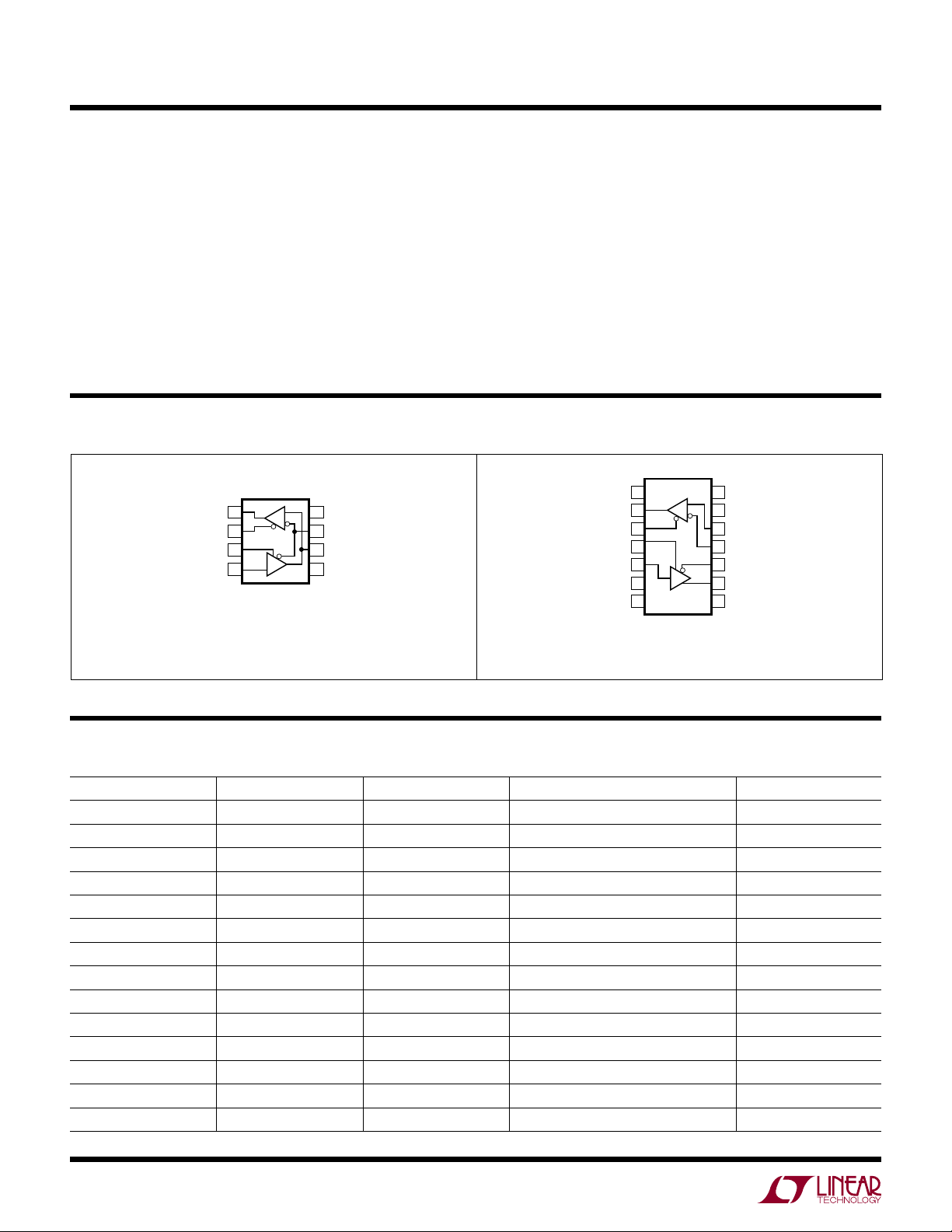
The LT1785/LT1785A are available in 8-lead DIP and SO
packages and the LT1791/LT1791A in 14-lead DIP and
SO packages.
-
Typical applicaTion
V
RO1
RE1
DE1
DI1
RO2
RE2
DE2
DI2
RX
LT1785
TX
RX
LT1785
TX
CC1
GND1
V
CC2
GND2
R
R
TERM
TERM
Normal Operation Waveforms at 250kBaud
RO
Y-Z
DI
178591 TA01
For more information www.linear.com/LT1785
178591 TA02
178591fd
1
Page 2
LT1785/LT1785A/
TOP VIEW
TOP VIEW
LT1791/LT1791A
absoluTe MaxiMuM raTings
(Note 1)
Supply Voltage (VCC) ................................................18V
Receiver Enable Input Voltage ...................... –0.3V to 6V
Driver Enable Input Voltage .......................... –0.3V to 6V
Driver Input Voltage ................................... –0.3V to 18V
Receiver Input Voltage ................................ –60V to 60V
Driver Output Voltage .................................. –60V to 60V
Receiver Output Voltage ...................–0.3V to (V
+ 6V)
CC
pin conFiguraTion
RO
1
2
3
4
R
D
8-LEAD PLASTIC SO
RE
DE
DI
N8 PACKAGE
8-LEAD PDIP
= 150°C, θJA = 130°C/W (N8)
T
JMAX
= 150°C, θJA = 150°C/W (S8)
T
JMAX
V
8
B
7
A
6
GND
5
S8 PACKAGE
CC
Operating Temperature Range
LT1785C/LT1791C/
LT1785AC/LT1791AC .................................... 0°C to 70°C
LT1785I/LT1791I/
LT1785AI/LT1791AI .................................. –40°C to 85°C
LT1785H/LT1791H/
LT1785AH/LT1791AH ............................. –40°C to 125°C
Storage Temperature Range ...................–65°C to 150°C
Lead Temperature (Soldering, 10 sec) .................. 300°C
1
NC
2
RO
3
RE
4
DE
5
DI
6
GND
7
GND
N PACKAGE
14-LEAD PDIP
= 150°C, θJA = 130°C/W (N)
T
JMAX
= 150°C, θJA = 150°C/W (S)
T
JMAX
14
V
CC
R
13
NC
12
A
11
B
10
9
8
S PACKAGE
Z
Y
NC
D
14-LEAD PLASTIC SO
orDer inForMaTion
LEAD FREE FINISH TAPE AND REEL PART MARKING* PACKAGE DESCRIPTION TEMPERATURE RANGE
LT1785CN8#PBF LT1785CN8#TRPBF 1785 8-Lead PDIP 0°C to 70°C
LT1785CS8#PBF LT1785CS8#TRPBF 1785 8-Lead Plastic SO 0°C to 70°C
LT1785IN8#PBF LT1785IN8#TRPBF 1785I 8-Lead PDIP –40°C to 85°C
LT1785IS8#PBF LT1785IS8#TRPBF 1785I 8-Lead Plastic SO –40°C to 85°C
LT1785ACN8#PBF LT1785ACN8#TRPBF 1785A 8-Lead PDIP 0°C to 70°C
LT1785ACS8#PBF LT1785ACS8#TRPBF 1785A 8-Lead Plastic SO 0°C to 70°C
LT1785AIN8#PBF LT1785AIN8#TRPBF 1785AI 8-Lead PDIP –40°C to 85°C
LT1785AIS8#PBF LT1785AIS8#TRPBF 1785AI 8-Lead Plastic SO –40°C to 85°C
LT1785HN8#PBF LT1785HN8#TRPBF 1785H 8-Lead PDIP –40°C to 125°C
LT1785HS8#PBF LT1785HS8#TRPBF 1785H 8-Lead Plastic SO –40°C to 125°C
LT1785AHN8#PBF LT1785AHN8#TRPBF 1785AH 8-Lead PDIP –40°C to 125°C
LT1785AHS8#PBF LT1785AHS8#TRPBF 1785AH 8-Lead Plastic SO –40°C to 125°C
LT1791CN#PBF LT1791CN#TRPBF 1791 14-Lead PDIP 0°C to 70°C
LT1791CS#PBF LT1791CS#TRPBF 1791 14-Lead Plastic SO 0°C to 70°C
2
For more information www.linear.com/LT1785
178591fd
Page 3
LT1785/LT1785A/
LT1791/LT1791A
orDer inForMaTion
LEAD FREE FINISH TAPE AND REEL PART MARKING* PACKAGE DESCRIPTION TEMPERATURE RANGE
LT1791IN#PBF LT1791IN#TRPBF 1791I 14-Lead PDIP –40°C to 85°C
LT1791IS#PBF LT1791IS#TRPBF 1791I 14-Lead Plastic SO –40°C to 85°C
LT1791ACN#PBF LT1791ACN#TRPBF 1791A 14-Lead PDIP 0°C to 70°C
LT1791ACS#PBF LT1791ACS#TRPBF 1791A 14-Lead Plastic SO 0°C to 70°C
LT1791AIN#PBF LT1791AIN#TRPBF 1791AI 14-Lead PDIP –40°C to 85°C
LT1791AIS#PBF LT1791AIS#TRPBF 1791AI 14-Lead Plastic SO –40°C to 85°C
LT1791HN#PBF LT1791HN#TRPBF 1791H 14-Lead PDIP –40°C to 125°C
LT1791HS#PBF LT1791HS#TRPBF 1791H 14-Lead Plastic SO –40°C to 125°C
LT1791AHN#PBF LT1791AHN#TRPBF 1791AH 14-Lead PDIP –40°C to 125°C
LT1791AHS#PBF LT1791AHS#TRPBF 1791AH 14-Lead Plastic SO –40°C to 125°C
LEAD BASED FINISH TAPE AND REEL PART MARKING* PACKAGE DESCRIPTION TEMPERATURE RANGE
LT1785CN8 LT1785CN8#TR 1785 8-Lead PDIP 0°C to 70°C
LT1785CS8 LT1785CS8#TR 1785 8-Lead Plastic SO 0°C to 70°C
LT1785IN8 LT1785IN8#TR 1785I 8-Lead PDIP –40°C to 85°C
LT1785IS8 LT1785IS8#TR 1785I 8-Lead Plastic SO –40°C to 85°C
LT1785ACN8 LT1785ACN8#TR 1785A 8-Lead PDIP 0°C to 70°C
LT1785ACS8 LT1785ACS8#TR 1785A 8-Lead Plastic SO 0°C to 70°C
LT1785AIN8 LT1785AIN8#TR 1785AI 8-Lead PDIP –40°C to 85°C
LT1785AIS8 LT1785AIS8#TR 1785AI 8-Lead Plastic SO –40°C to 85°C
LT1785HN8 LT1785HN8#TR 1785H 8-Lead PDIP –40°C to 125°C
LT1785HS8 LT1785HS8#TR 1785H 8-Lead Plastic SO –40°C to 125°C
LT1785AHN8 LT1785AHN8#TR 1785AH 8-Lead PDIP –40°C to 125°C
LT1785AHS8 LT1785AHS8#TR 1785AH 8-Lead Plastic SO –40°C to 125°C
LT1791CN LT1791CN#TR 1791 14-Lead PDIP 0°C to 70°C
LT1791CS LT1791CS#TR 1791 14-Lead Plastic SO 0°C to 70°C
LT1791IN LT1791IN#TR 1791I 14-Lead PDIP –40°C to 85°C
LT1791IS LT1791IS#TR 1791I 14-Lead Plastic SO –40°C to 85°C
LT1791ACN LT1791ACN#TR 1791A 14-Lead PDIP 0°C to 70°C
LT1791ACS LT1791ACS#TR 1791A 14-Lead Plastic SO 0°C to 70°C
LT1791AIN LT1791AIN#TR 1791AI 14-Lead PDIP –40°C to 85°C
LT1791AIS LT1791AIS#TR 1791AI 14-Lead Plastic SO –40°C to 85°C
LT1791HN LT1791HN#TR 1791H 14-Lead PDIP –40°C to 125°C
LT1791HS LT1791HS#TR 1791H 14-Lead Plastic SO –40°C to 125°C
LT1791AHN LT1791AHN#TR 1791AH 14-Lead PDIP –40°C to 125°C
LT1791AHS LT1791AHS#TR 1791AH 14-Lead Plastic SO –40°C to 125°C
Consult LTC Marketing for parts specified with wider operating temperature ranges. *The temperature grade is identified by a label on the shipping container.
For more information on lead free part marking, go to: http://www.linear.com/leadfree/
This product is only offered in trays. For more information go to: http://www.linear.com/packaging/
For more information www.linear.com/LT1785
178591fd
3
Page 4
LT1785/LT1785A/
LT1791/LT1791A
Dc elecTrical characTerisTics
The l denotes the specifications which apply over the full operating
temperature range, otherwise specifications are at TA = 25°C, VCC = 5V.
SYMBOL PARAMETER CONDITIONS MIN TYP MAX UNITS
V
OD1
V
OD2
V
OD
Differential Driver Output Voltage (Unloaded) IO = 0
Differential Driver Output Voltage (With Load) R = 50Ω (RS422), Figure 1
Change in Magnitude of Driver Differential Output
Voltage for Complementary Output States
V
∆|V
OC
Driver Common Mode Output Voltage R = 27Ω or R = 50Ω, Figure 1
| Change in Magnitude of Driver Common Mode Output
OC
Voltage for Complementary Output States
V
V
I
I
V
∆V
V
V
IH
IL
IN1
IN2
TH
OH
OL
Input High Voltage DI, DE, RE
Input Low Voltage DI, DE, RE
Input Current DI, DE, RE
Input Current (A, B); (LT1791 or LT1785 with DE = 0V) VIN = 12V
Differential Input Threshold Voltage for Receiver LT1785/LT1791: –7V ≤ VCM ≤ 12V
Receiver Input Hysteresis –7V < VCM < 12V 20 mV
TH
Receiver Output High Voltage IO = –400µA, VID = 200mV
Receiver Output Low Voltage IO = 1.6mA, VID = –200mV
Three-State (High Impedance) Output Current at
Receiver 0V < V
R
IN
Receiver Input Resistance (LT1791) –7V ≤ VCM ≤ 12V
OUT
< 6V
LT1785 –7V ≤ V
RS485 Unit Load 0.25
I
SC
Driver Short-Circuit Current V
Driver Output Fault Current V
Receiver Short-Circuit Current 0V ≤ V
Driver Three-State Output Current –7V ≤ V
I
CC
Supply Current No Load, RE = 0V, DE = 5V
R = 27Ω (RS485), Figure 1
R = 18Ω
R = 27Ω or R = 50Ω, Figure 1
R = 27Ω or R = 50Ω, Figure 1
V
= –7V
IN
–60V ≤ V
LT1785A/LT1791A: –7V ≤ V
≤ 60V
IN
CM
RE > 2V or Power Off
– 60V ≤ V
OUT
V
OUT
= 60V
O
V
= –60V
O
–60V ≤ V
≤ 60V
CM
≤ 12V
CM
= HIGH, Force VO = –7V
= LOW, Force VO = 12V
≤ V
O
CC
≤ 12V
O
≤ 60V
O
No Load, RE = 5V, DE = 5V
No Load, RE = 0V, DE = 0V
No Load, RE = 5V, DE = 0V
≤ 12V
l
l
2.0
l
1.5
l
1.2
l
l
2 2.5 3 V
l
l
2 V
l
l
l
l
–0.15
l
–6
l
–0.2
l
–0.2
l
3.5 4 V
l
l
–1 1 µA
l
85 125
4.1 5 V
2.70
2.45
2.2
0.15
–0.08
0.3 0.5 V
125
l
50 90 kΩ
l
35
l
35
l
l
–6
l
l
–0.2
l
–6
l
l
l
l
5.5
5.5
4.5
0.2
0.2 V
0.2 V
0.8 V
5 µA
0.3
6
mA
mA
mA
0.2
0
kΩ
kΩ
250
250
mA
mA
6 mA
mA
±35 mA
0.3
6
9
9
8
0.3
mA
mA
mA
mA
mA
mA
V
V
V
V
V
4
178591fd
For more information www.linear.com/LT1785
Page 5
LT1785/LT1785A/
LT1791/LT1791A
swiTching characTerisTics
The l denotes the specifications which apply over the full operating
temperature range, otherwise specifications are at TA = 25°C, VCC = 5V.
SYMBOL PARAMETER CONDITIONS MIN TYP MAX UNITS
t
PLH
t
PHL
t
SKEW
, t
t
r
f
t
ZH
t
ZL
t
LZ
t
HZ
t
PLH
t
PHL
t
SKD
t
ZL
t
ZH
t
LZ
t
HZ
f
MAX
t
SHDN
t
ZH(SHDN)
t
ZL(SHDN)
t
ZH(SHDN)
t
ZL(SHDN)
Driver Input to Output Figures 3, 5
Driver Input to Output Figures 3, 5
Driver Output to Output Figures 3, 5 100 ns
Driver Rise or Fall Time Figures 3, 5
Driver Enable to Output High Figures 4, 6
Driver Enable to Output Low Figures 4, 6
Driver Disable Time from Low Figures 4, 6
Driver Disable Time from High Figures 4, 6
Receiver Input to Output Figures 3, 7
Receiver Input to Output Figures 3, 7
Differential Receiver Skew 200 ns
Receiver Enable to Output Low Figures 2, 8
Receiver Enable to Output High Figures 2, 8
Receiver Disable from Low Figures 2, 8
Receiver Disable from High Figures 2, 8
Maximum Data Rate
Time to Shut Down Figures 2, 6, 8 3 µs
Driver Enable from Shutdown to Output High Figures 2, 6; RE = 5V 12 µs
Driver Enable from Shutdown to Output Low Figures 2, 6; RE = 5V 12 µs
Receiver Enable from Shutdown to Output High Figures 2, 8; DE = 0V 4 µs
Receiver Enable from Shutdown to Output Low Figures 2, 8; DE = 0V 4 µs
l
l
l
200 800 2000 ns
l
l
l
l
l
l
l
l
l
l
l
250 kbps
700 2000 ns
700 2000 ns
500 3000 ns
800 3000 ns
200 5000 ns
800 5000 ns
400 900 ns
400 900 ns
300 1000 ns
300 1000 ns
400 1000 ns
400 1000 ns
Note 1: Stresses beyond those listed under Absolute Maximum Ratings
may cause permanent damage to the device. Exposure to any Absolute
Maximum Rating condition for extended periods may affect device
reliability and lifetime.
178591fd
For more information www.linear.com/LT1785
5
Page 6

LT1785/LT1785A/
OUTPUT VOLTAGE (V)
4
DIFFERENTIAL VOLTAGE (V)
3.0
DELAY (ns)
1000
1000
I
(mA)
7
700
LT1791/LT1791A
Typical perForMance characTerisTics
Driver Differential Output Voltage
vs Load Resistance
TA = 25°C
3
2
1
0
10
100 1k
LOAD RESISTANCE (Ω)
Driver Propagation Delay
vs Temperature
900
800
700
600
500
400
300
PROPAGATION DELAY (ns)
200
100
0
–40
–20
LH
HL
0
TEMPERATURE (°C)
40
20
Driver Differential Output Voltage
vs Temperature
2.5
2.0
1.5
1.0
0.5
R = 27Ω
178591 G01
0
–40
–20
0
TEMPERATURE (°C)
40
20
60
80
178591 G02
100
LT1791 Driver Output Leakage
DE = 0V
1mA/DIV
–60V
80
178591 G04
100
60
V
IN
178591 G05
200µA/DIV
60V
Receiver Propagation Delay
vs Temperature
t
800
600
400
200
0
–40
–20
PHL
t
PLH
40
20
0
TEMPERATURE (°C)
LT1791 Receiver Input Current
vs V
IN
–60V
V
IN
80
178591 G03
178591 G06
100
60V
60
LT1785 Input Characteristics Pins
A or B; DE = RE = 0V
1mA/DIV
–60V
6
Supply Current vs Temperature
DRIVER AND
6
RECEIVER ON
5
RECEIVER ONLY
4
CC
3
2
V
, V
A
B
60V
178591 G07
1
0
–40
STANDBY
–20
0
TEMPERATURE (°C)
40
20
80
178591 G08
100
60
Receiver Propagation Delay
vs Differential Input Voltage
600
500
400
300
DELAY (ns)
LH VCM = 12V
200
100
0
0
HL VCM = 12V
1
VIN DIFFERENTIAL (V)
HL VCM = –7V
LH VCM = –7V
2
3 4
5
178591 G09
178591fd
For more information www.linear.com/LT1785
Page 7

pin FuncTions
LT1785/LT1785A/
LT1791/LT1791A
RO: Receiver Output. TTL level logic output. If the receiver
is active (RE pin low), RO is high if receiver input A ≥ B
by 200mV. If A ≤ B by 200mV, then RO will be low. RO
RE
assumes a high impedance output state when
or the part is powered off. RO is protected from output
shorts from ground to 6V.
RE: Receiver Output Enable. TTL level logic input. A logic
low on RE enables normal operation of the receiver output
RO. A logic high level at RE places the receiver output pin
RO into a high impedance state. If receiver enable RE and
driver enable DE are both in the disable state, the circuit
goes to a low power shutdown state. Placing either RE or
DE into its active state brings the circuit out of shutdown.
Shutdown state is not entered until a 3µs delay after both
RE and DE are disabled, allowing for logic skews in tog
gling between transmit and receive modes of operation.
For CAN bus applications, RE
the circuit from entering shutdown.
DE: Driver Output Enable. TTL level logic input. A logic
high on DE enables normal operation of the driver out
puts (Y and Z on LT1791, A and B on LT1785). A logic
low level at DE places the driver output pins into a high
impedance state. If receiver enable
DE are both in the disable state, the circuit goes to a low
power shutdown state. Placing either RE or DE into its
active state brings the circuit out of shutdown. Shutdown
state is not entered until a 3µs delay after both RE and DE
are disabled, allowing for logic skews in toggling between
transmit and receive modes of operation. For CAN bus
operation the DE pin is used for signal input to place the
data bus in dominant or recessive states.
DI: Driver Input. TTL level logic input. A logic high at DI
causes driver output A or Y to a high state, and output B
or Z to a low state. Complementary output states occur for
DI low. For CAN bus applications DI should be tied low.
GND: Ground.
should be tied low to prevent
RE
and driver enable
is high
-
-
-
Y: Driver Output. The Y driver output is in phase with the
driver input DI. In the LT1785 driver output Y is internally
connected to receiver input A. The driver output assumes
a high impedance state when DE is low, power is off or
thermal shutdown is activated. The driver output is pro
tected from shorts between ±60V in both active and high
impedance modes. For CAN applications, output Y is the
CANL output node.
Z: Driver Output. The Z driver output is opposite in phase
to the driver input DI. In the LT1785 driver output Z is
internally connected to receiver input B. The driver output
assumes a high impedance state when DE is low, power
is off or thermal shutdown is activated. The driver output
is protected from shorts between ±60V in both active and
high impedance modes. For CAN applications, output Z is
the CANH output node.
A: Receiver Input. The A receiver input forces a high receiver
output when V(A) ≥ [V(B) + 200mV]. V(A) ≤ [V(B)– 200mV]
forces a receiver output low. Receiver inputs A and B are
protected against voltage faults between ±60V. The high
input impedance allows up to 128 LT1785 or LT1791
transceivers on one RS485 data bus.
The LT1785A/LT1791A have guaranteed receiver input
thresholds –200mV < V
guaranteed to be in a high state for 0V inputs.
B: Receiver Input. The B receiver input forces a high
receiver output when V(A) ≥ [V(B) + 200mV]. When
V(A) ≤ [V(B) – 200mV], the B receiver forces a receiver
output low. Receiver inputs A and B are protected against
voltage faults between ±60V
allows up to 128 LT1785 or LT1791 transceivers on one
RS485 data bus.
The LT1785A/LT1791A have guaranteed receiver input
thresholds –200mV < VTH < 0. Receiver outputs are
guaranteed to be in a high state for 0V inputs.
: Positive Supply Input. For RS422 or RS485 operation,
V
CC
4.75V ≤ V
output drive swing. V
low ESR capacitor directly at Pin 8 (V
≤ 5.25V. Higher VCC input voltages increase
CC
CC
< 0. Receiver outputs are
TH
. The high input impedance
should be decoupled with a 0.1µF
).
CC
-
-
For more information www.linear.com/LT1785
178591fd
7
Page 8

LT1785/LT1785A/
A
S1
S1
LT1791/LT1791A
TesT circuiTs
R
V
OD
V
OC
R
B
1785/91 F01
RECEIVER
OUTPUT
TEST POINT
C
RL
1k
Figure 1. Driver DC Test Load Figure 2. Receiver Timing Test Load
5V
DE
DI
A
R
DIFF
B
A
C
L1
B
C
L2
RE
RO
15pF
1785/91 F03
OUTPUT
UNDER TEST
500Ω
C
L
Figure 3. Driver/Receiver Timing Test Circuit Figure 4. Driver Timing Test Load
1k
V
CC
S2
1785/91 F02
V
CC
S2
1785/91 F04
8
178591fd
For more information www.linear.com/LT1785
Page 9

FuncTion Tables
LT1785/LT1785A/
LT1791/LT1791A
LT1785 Transmitting
INPUTS OUTPUTS
RE DE DI A B RO
0 1 0 0 1 0
0 1 1 1 0 1
1 0 X Hi-Z Hi-Z Hi-Z
1 1 0 0 1 Hi-Z
1 1 1 1 0 Hi-Z
LT1785 Receiving
INPUTS OUTPUT
RE DE DI A-B RO
0 0 X ≤ –200mV 0
0 0 X ≥ 200mV* 1
0 0 X Open 1**
1 0 X X Hi-Z
* ≥ 0mV for LT1785A
** 1 for LT1785A; 1 or 0 for LT1785
LT1791
INPUTS OUTPUTS
RE DE DI A-B Y Z RO
0 0 X ≤ –200mV Hi-Z Hi-Z 0
0 0 X ≥ 200mV* Hi-Z Hi-Z 1
0 0 X Open Hi-Z Hi-Z 1**
0 1 0 ≤ –200mV 0 1 0
0 1 0 ≥ 200mV* 0 1 1
0 1 0 Open 0 1 1**
0 1 1 ≤ –200mV 1 0 0
0 1 1 ≥ 200mV* 1 0 1
0 1 1 Open 1 0 1**
1 0 X X Hi-Z Hi-Z Hi-Z
1 1 0 X 0 1 Hi-Z
1 1 1 X 1 0 Hi-Z
* ≥ 0mV for LT1791A
** 1 for LT1791A; 1 or 0 for LT1791
For more information www.linear.com/LT1785
178591fd
9
Page 10

LT1785/LT1785A/
5V
5V
LT1791/LT1791A
swiTching TiMe waVeForMs
DI
DE
A, B
A, B
5V
0V
B
A
V
O
0V
–V
O
V
O
1/2 V
1.5V
O
10%
t
r
f = 125kHz, tr ≤ 10ns, tf ≤ 10ns
t
PLH
t
SKEW
90%
V
DIFF
= V(A) – V(B)
1.5V
1/2 V
t
PHL
t
SKEW
90%
10%
t
f
O
1785/91 F05
Figure 5. Driver Propagation Delays
0V
5V
V
OL
V
OH
0V
1.5V
f = 125kHz, tr ≤ 10ns, tf ≤ 10ns
t
ZL(SHDN), tZL
2.3V
2.3V
OUTPUT NORMALLY LOW
OUTPUT NORMALLY HIGH
t
ZH(SHDN), tZH
1.5V
t
LZ
0.5V
0.5V
t
HZ
178591 F06
Figure 6. Driver Enable and Disable Times
V
RO
A – B
OH
V
OL
V
OD2
–V
OD2
t
PHL
1.5V
f = 125kHz, tr ≤ 10ns, tf ≤ 10ns
0V 0V
OUTPUT
INPUT
t
PLH
1.5V
178591 F07
Figure 7. Receiver Propagation Delays
RE
0V
5V
RO
RO
0V
1.5V
f = 125kHz, tr ≤ 10ns, tf ≤ 10ns
t
, t
1.5V
1.5V
ZL(SHDN)
t
ZH(SHDN)
ZL
OUTPUT NORMALLY LOW
OUTPUT NORMALLY HIGH
, t
ZH
t
t
1.5V
LZ
0.5V
0.5V
HZ
178591 F08
10
Figure 8. Receiver Enable and Disable Times
178591fd
For more information www.linear.com/LT1785
Page 11

applicaTions inForMaTion
LT1785/LT1785A/
LT1791/LT1791A
Overvoltage Protection
The LT1785/LT1791 RS485/RS422 transceivers answer an
applications need for overvoltage fault tolerance on data
networks. Industrial installations may encounter common
mode voltages between nodes far greater than the –7V to
12V range specified for compliance to RS485 standards.
CMOS RS485 transceivers can be damaged by voltages
above their absolute maximum ratings of typically –8V
to 12.5V. Replacement of standard RS485 transceiver
components with the LT1785 or LT1791 devices eliminates
field failures due to overvoltage faults or the use of costly
external protection devices. The limited overvoltage toler
ance of CMOS RS485 transceivers makes implementation
of effective external protection networks difficult without
interfering with proper data network performance within
the –7V to 12V region of RS485 operation.
The high overvoltage rating of the LT1785/LT1791 facili
tates easy extension to almost any level. Simple discrete
component
driver output voltages to less than ±60V can be added
to the device to extend protection to any desired level.
Figure 11 shows a protection network against faults to
the120VAC line voltage.
The LT1785/LT1791 protection is achieved by using a high
voltage bipolar integrated circuit process for the transceiv
ers. The naturally high breakdown voltages of the bipolar
process provides protection in powered-off and high
impedance
current limit design to protect against overvoltage faults
while still allowing high current output drive.
ESD Protection
The LT1785/LT1791 I/O pins have on-chip ESD protection
circuitry to eliminate field failures caused by discharges to
exposed ports and cables in application environments. The
networks
conditions.
that limit the receiver input and
The driver outputs use a foldback
-
-
-
LT1785 pins A and B and the LT1791 driver output pins Y
and Z are protected to IEC-1000-4-2 level 2. These pins will
survive multiple ESD strikes of ±15kV air discharge or ±4kV
contact discharge. Due to their very high input impedance,
the LT1791 receiver pins are protected to IEC-1000-4-2
level 2, or ±15kV air and ±4kV contact discharges. This
level of ESD protection will guarantee immunity from field
failures in all but the most severe ESD environments. The
LT1791 receiver input ESD tolerance may be increased to
IEC level 4 compliance by adding 2.2k resistors in series
with these pins.
Low Power Shutdown
The LT1785/LT1791 have RE and DE logic inputs to control
the receive and transmit modes of the transceivers. The
RE input allows normal data reception when in the low
state. The receiver output goes to a high impedance state
when RE is high, allowing multiplexing the RO data line.
The DE logic input performs a similar function on the driver
outputs. A high state on DE activates the differential driver
outputs, a low state places both driver outputs in to high
impedance. Tying the RE and DE logic inputs together may
be done to allow one logic signal to toggle the transceiver
from receive to transmit modes. The DE input is used as
the data input in CAN bus applications.
Disabling both the driver and receiver places the device
into a low supply current shutdown mode. An internal
time delay of 3µs minimum prevents entering shutdown
due to small logic skews when a toggle between receive
and transmit is desired. The recovery time from shutdown
mode is typically 12µs. The user must be careful to allow
for this wake-up delay from shutdown mode. To allow full
250kbaud data rate transmission in CAN applications, the
RE pin should be tied low to prevent entering shutdown
mode.
For more information www.linear.com/LT1785
178591fd
11
Page 12

LT1785/LT1785A/
LT1791/LT1791A
applicaTions inForMaTion
Slew Limiting for EMI Emissions Control
The LT1785/LT1791 feature controlled driver output slew
rates to control high frequency EMI emissions from equip
-
ment and data cables. The slew limiting limits data rate
operation to 250kbaud. Slew limiting also mitigates the
adverse affects of imperfect transmission line termina
-
tion caused by stubs or mismatched cable. In some low
speed, short distance networks, cable termination may
be eliminated completely with no adverse effect on data
transmission.
12
A
RX
TX
120Ω
11
B
10
Z
9
Y
RO
RE
DE
2
3
4
5
DI
Data Network Cable Selection and Termination
Long distance data networks operating at high data trans
mission rates should use high quality, low attenuation
cable with well-matched cable terminations. Short distance
networks at low data rates may use much less expensive
P
VC cable. These cables have characteristic impedances
as low as 72Ω. The LT1785/LT1791 output drivers are
guaranteed to drive cables as low as 72Ω.
9
120Ω
Y
10
Z
LT1791LT1791
B
11
12
RX
A
5
4
3
2
DI
DE
RE
RO
178591 F09
TX
Figure 9. Full-Duplex RS422
12
178591fd
For more information www.linear.com/LT1785
Page 13

package DescripTion
(0.508)
.400*
NOTE:
1. DIMENSIONS ARE
*THESE DIMENSIONS DO NOT INCLUDE MOLD FLASH OR PROTRUSIONS.
MOLD FLASH OR PROTRUSIONS SHALL NOT EXCEED .010 INCH (0.254mm)
N8 Package
8-Lead PDIP (Narrow 0.300)
(LTC DWG # 05-08-1510)
87 6
.255 ± .015*
(6.477 ± 0.381)
LT1785/LT1785A/
LT1791/LT1791A
(10.160)
MAX
5
12
.300 – .325
(7.620 – 8.255)
.065
(1.651)
.008 – .015
(0.203 – 0.381)
+.035
.325
–.015
+0.889
8.255
()
–0.381
INCHES
MILLIMETERS
TYP
.045 – .065
(1.143 – 1.651)
.100
(2.54)
BSC
3
4
.130 ± .005
(3.302 ± 0.127)
.120
(3.048)
MIN
.018 ± .003
(0.457 ± 0.076)
.020
MIN
N8 1002
For more information www.linear.com/LT1785
178591fd
13
Page 14

LT1785/LT1785A/
(0.101 – 0.254)
.189 – .197
.030
MOLD FLASH OR PROTRUSIONS SHALL NOT EXCEED .006" (0.15mm)
LT1791/LT1791A
package DescripTion
S8 Package
8-Lead Plastic Small Outline (Narrow 0.150)
(LTC DWG # 05-08-1610)
.050 BSC
.245
MIN
±.005
TYP
RECOMMENDED SOLDER PAD LAYOUT
.010 – .020
(0.254 – 0.508)
.008 – .010
(0.203 – 0.254)
NOTE:
1. DIMENSIONS IN
2. DRAWING NOT TO SCALE
3. THESE DIMENSIONS DO NOT INCLUDE MOLD FLASH OR PROTRUSIONS.
× 45°
.016 – .050
(0.406 – 1.270)
INCHES
(MILLIMETERS)
.045 ±.005
.160
±.005
0°– 8° TYP
.228 – .244
(5.791 – 6.197)
.053 – .069
(1.346 – 1.752)
.014 – .019
(0.355 – 0.483)
TYP
(4.801 – 5.004)
8
1
NOTE 3
7
2
5
6
.150 – .157
(3.810 – 3.988)
NOTE 3
3
4
.004 – .010
.050
(1.270)
BSC
SO8 0303
14
178591fd
For more information www.linear.com/LT1785
Page 15

package DescripTion
(1.651)
.770*
NOTE:
1. DIMENSIONS ARE
*THESE DIMENSIONS DO NOT INCLUDE MOLD FLASH OR PROTRUSIONS.
MOLD FLASH OR PROTRUSIONS SHALL NOT EXCEED .010 INCH (0.254mm)
N Package
14-Lead PDIP (Narrow 0.300)
(LTC DWG # 05-08-1510)
14
.255 ± .015*
(6.477 ± 0.381)
1213
(19.558)
MAX
11
LT1785/LT1785A/
LT1791/LT1791A
8910
31
2
.300 – .325
(7.620 – 8.255)
(0.508)
.008 – .015
(0.203 – 0.381)
+.035
.325
–.015
+0.889
8.255
()
–0.381
INCHES
MILLIMETERS
.020
MIN
.130 ± .005
(3.302 ± 0.127)
.120
(3.048)
MIN
.005
(0.127)
MIN
(1.143 – 1.651)
.100
(2.54)
BSC
4
.045 – .065
6
7
.065
TYP
.018 ± .003
(0.457 ± 0.076)
N14 1103
5
For more information www.linear.com/LT1785
178591fd
15
Page 16

LT1785/LT1785A/
(3.810 – 3.988)
.337 – .344
.030
MOLD FLASH OR PROTRUSIONS SHALL NOT EXCEED .006" (0.15mm)
LT1791/LT1791A
package DescripTion
S Package
14-Lead Plastic Small Outline (Narrow 0.150)
(LTC DWG # 05-08-1610)
.050 BSC
N
.245
MIN
123 N/2
±.005
TYP
RECOMMENDED SOLDER PAD LAYOUT
.010 – .020
(0.254 – 0.508)
.008 – .010
(0.203 – 0.254)
NOTE:
1. DIMENSIONS IN
2. DRAWING NOT TO SCALE
3. THESE DIMENSIONS DO NOT INCLUDE MOLD FLASH OR PROTRUSIONS.
× 45°
.016 – .050
(0.406 – 1.270)
INCHES
(MILLIMETERS)
.045 ±.005
±.005
.160
0° – 8° TYP
.228 – .244
(5.791 – 6.197)
.053 – .069
(1.346 – 1.752)
14
N
1
.014 – .019
(0.355 – 0.483)
TYP
13
2
(8.560 – 8.738)
NOTE 3
12
11 10
3
4
.050
(1.270)
BSC
8
9
.150 – .157
N/2
5
7
6
NOTE 3
.004 – .010
(0.101 – 0.254)
S14 0502
16
178591fd
For more information www.linear.com/LT1785
Page 17

LT1785/LT1785A/
LT1791/LT1791A
reVision hisTory
REV DATE DESCRIPTION PAGE NUMBER
D 03/15 Added notes to Function Tables 9
(Revision history begins at Rev D)
Information furnished by Linear Technology Corporation is believed to be accurate and reliable.
However, no responsibility is assumed for its use. Linear Technology Corporation makes no representation that the interconnection of its circuits as described herein will not infringe on existing patent rights.
For more information www.linear.com/LT1785
178591fd
17
Page 18

LT1785/LT1785A/
RAYCHEM
LT1791/LT1791A
Typical applicaTion
RO
1
RX
2
RE
DE
DI
LT1785
3
4
TX
R
T
120Ω
7
B
6
A
6
7
A
B
LT1785
4
DI
DE
1
3
2
RE
RO
6
7
A
B
LT1785
4
3
DI
DE
1
2
RE
RO
R
120Ω
T
7
6
RX
B
A
LT1785
1
RO
2
RE
3
DE
4
TX
DI
178591 F10
Figure 10. Half-Duplex RS485 Network Operation
POLYSWITCH
TR600-150
× 2
COMPOSITE
47Ω
47Ω
CARBON
5W
0.1µF
300V
RT,120Ω
178591 F11
RO
RE
DE
8
V
1
RX
2
LT1785
3
4
DI
TX
CC
7
B
6
A
5
1.5KE36CA
Figure 11. RS485 Network with 120V AC Line Fault Protection
relaTeD parTs
PART NUMBER DESCRIPTION COMMENTS
LTC2854/LTC2855 3.3V 20Mbps RS485/RS422 Transceivers with Integrated
Switchable Termination
LTC2856/LTC2857/
LTC2858
LTC2850/LTC2851/
5V 20Mbps and Slew Rate Limited 15kV RS485/RS422
Transceivers
3.3V 20Mbps RS485/RS422 Transceivers ±15kV ESD, 125°C Operation
LTC2852
LTC2859/LTC2861 20Mbps RS485 Transceivers with Integrated Switchable
Termination
LTC2862/LTC2863/
±60V Fault Protected 3V to 5.5V RS485/RS422 Transceivers 20Mbps or 250kbps, ±15kV HBM ESD, ±25V Common Mode
LTC2864/LTC2865
LTM2881 Complete 3.3V Isolated RS485/RS422 µModule
®
Transceiver
+ Power
Linear Technology Corporation
18
1630 McCarthy Blvd., Milpitas, CA 95035-7417
(408) 432-1900 ● FAX: (408) 434-0507
For more information www.linear.com/LT1785
●
www.linear.com/LT1785
Up to ±25kV HBM ESD, 125°C Operation
±15kV ESD, 125°C Operation
Integrated, Switchable,120Ω Termination Resistor, ±15kV ESD
Range
2500V
Isolation with Integrated Isolated DC/DC Converter and
RMS
Switchable Termination
178591fd
LT 0315 REV D • PRINTED IN USA
LINEAR TECHNOLOGY CORPORATION 1998
 Loading...