


OUTPUT CURRENT (mA)
0
0
DROPOUT VOLTAGE (V)
0.1
0.2
0.3
0.4
0.6
50
100 150 200
LT1521 • TA02
250 300
0.5
FEATURES
LT1521/LT1521-3
LT1521-3.3/LT1521-5
300mA Low Dropout
Regulators with Micropower
Quiescent Current and Shutdown
U
DESCRIPTIO
■
Dropout Voltage: 0.5V
■
Output Current: 300mA
■
Quiescent Current: 12µA
■
No Protection Diodes Needed
■
Adjustable Output from 3.8V to 20V
■
Fixed Output Voltages: 3V, 3.3V, 5V
■
Controlled Quiescent Current in Dropout
■
Shutdown IQ = 6µA
■
Reverse Battery Protection
■
No Reverse Current
■
Thermal Limiting
U
APPLICATIO S
■
Low Current Regulator
■
Regulator for Battery-Powered Systems
■
Post Regulator for Switching Supplies
The LT®1521/LT1521-3/LT1521-3.3/LT1521-5 are low
dropout regulators with micropower quiescent current
and shutdown. These devices are capable of supplying
300mA of output current with a dropout voltage of 0.5V.
Designed for use in battery-powered systems, the low
quiescent current, 12µA operating and 6µA in
shutdown, makes them an ideal choice. The quiescent
current is well controlled; it does not rise in dropout as it
does with many other low dropout PNP regulators.
Other features of the LT1521/LT1521-3/LT1521-3.3/
LT1521-5 include the ability to operate with very small
output capacitors. They are stable with only 1.5µF on the
output while most older devices require between 10µF and
100µF for stability. Small ceramic capacitors can be used,
enhancing manufacturability. Also, the input may be connected to voltages lower than the output voltage, including
negative voltages, without reverse current flow from output to input. This makes the LT1521 series ideal for backup
power situations where the output is held high and the
input is low or reversed. Under these conditions only 5µA
will flow from the output pin to ground.
, LTC and LT are registered trademarks of Linear Technology Corporation.
TYPICAL APPLICATIO
U
5V Battery-Powered Supply with Shutdown
6V 1.5µF1µF
8
IN
5
SHDN
V
SHDN
<0.25 OFF
>2.80 ON
LT1521-5
GND
3
(PIN 5) OUTPUT
NC ON
OUT
SENSE
1
2
Dropout Voltage
5V
300mA
+
LT1521 • TA01
1521335fb
1

LT1521/LT1521-3
LT1521-3.3/LT1521-5
WW
W
ABSOLUTE MAXIMUM RATINGS
U
(Note 1)
Input Voltage ...................................................... ±20V*
Output Pin Reverse Current .................................. 10mA
Adjust Pin Current ................................................ 10mA
Shutdown Pin Input Voltage (Note 1) ..........6.5V, –0.6V
Shutdown Pin Input Current (Note 1) ..................... 5mA
Output Short-Circuit Duration.......................... Indefinite
U
W
U
PACKAGE/ORDER INFORMATION
TOP VIEW
OUT
SENSE/ADJ*
1
2
NC
3
GND
4
MS8 PACKAGE
8-LEAD PLASTIC MSOP
*PIN 2 = SENSE FOR LT1521-3/
LT1521-3.3/LT1521-5
PIN 2 = ADJ FOR LT1521
T
= 125°C, θJA = 125°C/W
JMAX
8
7
6
5
IN
NC
NC
SHDN
SENSE/ADJ*
*PIN 2 = SENSE FOR LT1521-3/LT1521-3.3/LT1521-5
SEE THE APPLICATIONS INFORMATION SECTION
1
OUT
2
GND
3
NC
4
8-LEAD PLASTIC SO
= ADJ FOR LT1521
T
= 125°C, θJA = 70°C/W
JMAX
Storage Temperature Range ................. –65°C to 150°C
Operating Junction Temperature Range (Note 2)
Commercial ...........................................0°C to 125°C
Industrial ......................................... – 40°C to 125°C
Lead Temperature (Soldering, 10 sec)..................300°C
*For applications requiring input voltage ratings greater than 20V, contact
the factory.
TOP VIEW
S8 PACKAGE
8
IN
GND
7
GND
6
SHDN
5
TAB IS
SEE THE APPLICATIONS INFORMATION SECTION
FRONT VIEW
GND
ST PACKAGE
3-LEAD PLASTIC SOT-223
T
= 125°C, θJA = 50°C/W
JMAX
3
OUT
2
GND
1
IN
ORDER PART NUMBER
LT1521CMS8
LT1521CMS8-3
LT1521CMS8-3.3
LT1521CMS8-5
ORDER PART NUMBER
LT1521CS8
LT1521CS8-3
LT1521CS8-3.3
LT1521CS8-5
LT1521IS8
LT1521IS8-3
LT1521IS8-3.3
LT1521IS8-5
MS8 PART MARKING
LTEZ
LTFB
LTDU
LTFA
Consult LTC Marketing for parts specified with wider operating temperature ranges.
S8 PART MARKING
1521
15213
152133
15215
1521I
1521I3
1521I33
1521I5
ORDER PART NUMBER
LT1521CST-3
LT1521CST-3.3
LT1521CST-5
LT1521IST-3
LT1521IST-3.3
LT1521IST-5
ST PART MARKING
15213
152133
15215
1521I3
1521I33
1521I5
2
1521335fb

LT1521/LT1521-3
LT1521-3.3/LT1521-5
ELECTRICAL CHARACTERISTICS
The ● denotes the specifications which apply over the full operating
temperature range, otherwise specifications are at TA = 25°C.
PARAMETER CONDITIONS MIN TYP MAX UNITS
Regulated Output Voltage LT1521-3 VIN = 3.5V, I
(Note 4) 4V < VIN < 20V, 1mA < I
LT1521-3.3 VIN = 3.8V, I
4.3V < VIN < 20V, 1mA < I
LT1521-5 VIN = 5.5V, I
6V < VIN < 20V, 1mA < I
LT1521 (Note 5) VIN = 4.3V, I
4.8V < VIN < 20V, 1mA < I
Line Regulation LT1521-3 ∆VIN = 4.5 to 20V, I
LT1521-3.3 ∆VIN = 4.8 to 20V, I
LT1521-5 ∆VIN = 5.5 to 20V, I
LT1521 (Note 5) ∆VIN = 4.3 to 20V, I
Load Regulation LT1521-3 ∆I
LT1521-3.3 ∆I
LT1521-5 ∆I
LT1521 (Note 5) ∆I
LT1521-3 ∆I
LT1521-3.3 ∆I
LT1521-5 ∆I
LT1521 (Note 5) ∆I
Dropout Voltage (Note 6) I
Ground Pin Current (Note 7) I
= 1mA, TJ = 25°C 130 170 mV
LOAD
I
= 1mA ● 250 mV
LOAD
I
= 50mA, TJ = 25°C 290 350 mV
LOAD
I
= 50mA ● 450 mV
LOAD
I
= 100mA, TJ = 25°C 350 420 mV
LOAD
I
= 100mA ● 550 mV
LOAD
I
= 150mA, TJ = 25°C 400 470 mV
LOAD
I
= 150mA ● 600 mV
LOAD
I
= 300mA, TJ = 25°C 500 600 mV
LOAD
I
= 300mA ● 750 mV
LOAD
= 0mA ● 12 25 µA
LOAD
I
= 1mA ● 65 100 µA
LOAD
I
= 10mA ● 300 450 µA
LOAD
I
= 50mA ● 0.8 1.5 mA
LOAD
I
= 100mA ● 1.4 2.5 mA
LOAD
I
= 150mA ● 2.2 4.0 mA
LOAD
I
= 300mA ● 6.5 12.0 mA
LOAD
LOAD
LOAD
LOAD
LOAD
LOAD
LOAD
LOAD
LOAD
Adjust Pin Bias Current (Notes 5, 8) TJ = 25°C 50 100 nA
Shutdown Threshold V
Shutdown Pin Current (Note 9) V
Quiescent Current in Shutdown (Note 10) VIN = V
Ripple Rejection VIN – V
Current Limit VIN – V
= Off to On ● 1.20 2.80 V
OUT
V
= On to Off ● 0.25 0.75 V
OUT
= 0V ● 2.0 5.0 µA
SHDN
(NOMINAL) + 1V, V
OUT
= 1V(Avg), V
f
RIPPLE
VIN = V
OUT
= 120Hz, I
= 7V, TJ = 25°C 400 800 mA
OUT
(NOMINAL) + 1.5V, ∆V
OUT
LOAD
RIPPLE
= 150mA
= 1mA, TJ = 25°C 2.950 3.000 3.050 V
OUT
= 1mA, TJ = 25°C 3.250 3.300 3.350 V
OUT
= 1mA, TJ = 25°C 4.925 5.000 5.075 V
OUT
= 1mA, TJ = 25°C 3.695 3.750 3.805 V
OUT
< 300mA ● 2.900 3.000 3.100 V
OUT
< 300mA ● 3.200 3.300 3.400 V
OUT
< 300mA ● 4.850 5.000 5.150 V
OUT
< 300mA ● 3.640 3.750 3.860 V
OUT
= 1mA ● 1.5 20 mV
OUT
= 1mA ● 1.5 20 mV
OUT
= 1mA ● 1.5 20 mV
OUT
= 1mA ● 1.5 20 mV
OUT
= 1mA to 300mA, TJ ≤ 25°C–20–30mV
= 1mA to 300mA, TJ ≤ 25°C–20–30mV
= 1mA to 300mA, TJ ≤ 25°C–25–45mV
= 1mA to 300mA, TJ ≤ 25°C–20–30mV
= 1mA to 300mA, TJ >25°C–20–55mV
= 1mA to 300mA, TJ > 25°C–20–55mV
= 1mA to 300mA, TJ > 25°C–25–75mV
= 1mA to 300mA, TJ > 25°C–20–55mV
= 0V ● 612µA
SHDN
= 0.5V
,5058dB
P–P
= –0.1V ● 320 400 mA
OUT
1521335fb
3

LT1521/LT1521-3
LT1521-3.3/LT1521-5
ELECTRICAL CHARACTERISTICS
The ● denotes the specifications which apply over the full operating
temperature range, otherwise specifications are at TA = 25°C.
PARAMETER CONDITIONS MIN TYP MAX UNITS
Input Reverse Leakage Current VIN = –20V, V
Reverse Output Current (Note 11) LT1521-3 V
LT1521-3.3 V
LT1521-5 V
LT1521 (Note 5) V
Note 1: Absolute Maximum Ratings are those values beyond which the life
of a device may be impaired.
Note 2: The shutdown pin input voltage rating is required for a low
impedance source. Internal protection devices connected to the shutdown
pin will turn on and clamp the pin to approximately 7V or –0.6V. This
range allows the use of 5V logic devices to drive the pin directly. For high
impedance sources or logic running on supply voltages greater than 5.5V,
the maximum current driven into the shutdown pin must be limited to less
than 5mA.
Note 3: For junction temperatures greater than 110°C, a minimum load of
1mA is recommended. For T
> 110°C and I
J
< 1mA, output voltage
OUT
may increase by 1%.
Note 4: Operating conditions are limited by maximum junction
temperature. The regulated output voltage specification will not apply for
all possible combinations of input voltage and output current. When
operating at maximum input voltage, the output current range must be
limited. When operating at maximum output current, the input voltage
range must be limited.
= 0V ● 1.0 mA
OUT
= 3V, VIN < 3V, TJ = 25°C510µA
OUT
= 3.3V, VIN < 3.3V, TJ = 25°C510µA
OUT
= 5V, VIN < 5V, TJ = 25°C510µA
OUT
= 3.8V, VIN < 3.75V, TJ = 25°C510µA
OUT
Note 5: The LT1521 (adjustable version) is tested and specified with the
adjust pin connected to the output pin.
Note 6: Dropout voltage is the minimum input/output voltage required to
maintain regulation at the specified output current. In dropout the output
voltage will be equal to: (V
IN
– V
Note 7: Ground pin current is tested with V
DROPOUT
)
= V
IN
(nominal) and a
OUT
current source load. This means the device is tested while operating in its
dropout region. This is the worst-case ground pin current. The ground pin
current will decrease slightly at higher input voltages.
Note 8: Adjust pin bias current flows into the adjust pin.
Note 9: Shutdown pin current at V
= 0V flows out of the shutdown
SHDN
pin.
Note 10: Quiescent current in shutdown is equal to the total sum of the
shutdown pin current (2µA) and the ground pin current (4µA).
Note 11: Reverse output current is tested with the input pin grounded and
the output pin forced to the rated output voltage. This current flows into
the output pin and out of the ground pin.
W
U
TYPICAL PERFORMANCE CHARACTERISTICS
Guaranteed Dropout Voltage
0.8
= TEST POINTS
0.7
0.6
0.5
0.4
0.3
DROPOUT VOLTAGE (V)
0.2
0.1
TJ ≤ 125°C
0
50 100 200
0
OUTPUT CURRENT (mA)
TJ ≤ 25°C
150
250
LT1521 • TPC01
300
Dropout Voltage
0.8
0.7
0.6
0.5
0.4
0.3
DROPOUT VOLTAGE (V)
0.2
0.1
0
–25 0 50
–50
TEMPERATURE (°C)
I
I
LOAD
LOAD
= 300mA
= 100mA
I
LOAD
I
LOAD
25
I
LOAD
= 50mA
= 1mA
75 100 125
= 150mA
4
LT1521 • TPC02
Quiescent Current
15.0
12.5
10.0
7.5
5.0
QUIESCENT CURRENT (µA)
2.5
0
–50
VIN = 6V
= ∞
R
L
I
LOAD
–25 0
= 0
25 75
TEMPERATURE (°C)
V
= OPEN
SHDN
V
= 0V
SHDN
50 100 125
LT1521 • TPC03
1521335fb

W
U
TYPICAL PERFORMANCE CHARACTERISTICS
LT1521/LT1521-3
LT1521-3.3/LT1521-5
LT1521-3
Output Voltage
3.08
3.06
3.04
3.02
3.00
2.98
OUTPUT VOLTAGE (V)
2.96
2.94
2.92
–25 0 50
–50
LT1521
Adjust Pin Voltage
3.83
I
= 1mA
LOAD
3.81
3.79
3.77
3.75
3.73
OUTPUT VOLTAGE (V)
3.71
3.69
3.67
–25 0 50
–50
25
TEMPERATURE (°C)
25
TEMPERATURE (°C)
75 100 125
LT1521 • TPC04
75 100 125
LT1521 • TPC07
LT1521-3.3
Output Voltage
3.38
I
= 1mA
OUT
3.36
3.34
3.32
3.30
3.28
OUTPUT VOLTAGE (V)
3.26
3.24
3.22
–25 0 50
–50
LT1521-3
Quiescent Current
50
45
40
35
30
25
20
15
QUIESCENT CURRENT (µA)
10
5
0
213579
0
25
TEMPERATURE (°C)
V
= OPEN
SHDN
V
= 0V
SHDN
6
4
INPUT VOLTAGE (V)
75 100 125
LT1521 • TPC05
TJ = 25°C
=
∞
R
L
8
LT1521 • TPC08
OUTPUT VOLTAGE (V)
10
LT1521-5
Output Voltage
5.08
5.06
5.04
5.02
5.00
4.98
4.96
4.94
4.92
–25 0 50
–50
LT1521-3.3
Quiescent Current
50
45
40
35
30
25
20
15
QUIESCENT CURRENT (µA)
10
5
0
213579
0
25
TEMPERATURE (°C)
6
4
INPUT VOLTAGE (V)
75 100 125
LT1521 • TPC06
TJ = 25°C
=
∞
R
L
8
LT1521 • TPC09
10
LT1521-5
Quiescent Current
50
45
40
35
30
25
20
15
QUIESCENT CURRENT (µA)
10
5
0
213579
0
V
SHDN
V
= 0V
SHDN
6
4
INPUT VOLTAGE (V)
TJ = 25°C
R
=
L
= OPEN
8
LT1521 • TPC10
LT1521
Quiescent Current
50
∞
10
45
40
35
30
25
20
15
QUIESCENT CURRENT (µA)
10
5
0
0
V
SHDN
213579
4
INPUT VOLTAGE (V)
V
SHDN
= 0V
6
TJ = 25°C
= OPEN
=
R
L
8
LT1521 • TPC11
∞
10
LT1521-3
Ground Pin Current
1000
TJ = 25°C
900
*FOR V
800
700
600
500
400
300
GROUND PIN CURRENT (µA)
200
100
0
0
OUT
213579
= 3V
R
I
R
= 120Ω
LOAD
= 25mA*
I
LOAD
R
LOAD
I
LOAD
R
= 3k
LOAD
= 1mA*
I
LOAD
6
4
INPUT VOLTAGE (V)
LOAD
LOAD
= 300Ω
= 10mA*
= 60Ω
= 50mA*
8
LT1521 • TPC12
1521335fb
10
5

LT1521/LT1521-3
TEMPERATURE (°C)
–50
SHUTDOWN PIN THRESHOLD (V)
2.0
1.8
1.6
1.4
1.2
1.0
0.8
0.6
0.4
0.2
0
0
50
75
LT1521 • TPC21
–25
25
100
125
I
LOAD
= 1mA
INPUT VOLTAGE (V)
0
GROUND PIN CURRENT (mA)
8
7
6
5
4
3
2
1
0
8
LT1521 • TPC15
2
4
6
10
7
1
3
5
9
R
LOAD
= 11Ω
I
LOAD
= 300mA*
R
LOAD
= 22Ω
I
LOAD
= 150mA*
R
LOAD
= 33Ω
I
LOAD
= 100mA*
TJ = 25°C
*FOR V
OUT
= 3.3V
LT1521-3.3/LT1521-5
W
U
TYPICAL PERFORMANCE CHARACTERISTICS
LT1521-3
Ground Pin Current
8
7
6
5
4
3
2
GROUND PIN CURRENT (mA)
1
0
2
1
0
4
3
INPUT VOLTAGE (V)
LT1521-5
Ground Pin Current
1000
TJ = 25°C
900
*FOR V
800
700
600
500
400
300
GROUND PIN CURRENT (µA)
200
100
0
0
= 5V
OUT
213579
4
INPUT VOLTAGE (V)
R
I
LOAD
5
LOAD
TJ = 25°C
*FOR V
R
LOAD
I
LOAD
R
LOAD
I
LOAD
R
= 30Ω
LOAD
= 100mA*
I
LOAD
6
7
R
LOAD
I
LOAD
R
LOAD
I
LOAD
= 500Ω
= 10mA*
R
LOAD
I
LOAD
6
= 3V
OUT
= 10Ω
= 300mA*
= 20Ω
= 150mA*
8
9
LT1521 • TPC13
= 100Ω
= 50mA*
= 200Ω
= 25mA*
= 5k
= 1mA*
8
LT1521 • TPC16
LT1521-3.3
Ground Pin Current
1000
900
800
700
600
500
400
300
GROUND PIN CURRENT (µA)
200
100
0
10
0
R
LOAD
I
LOAD
R
I
LOAD
213579
INPUT VOLTAGE (V)
= 66Ω
= 50mA*
= 3.3k
LOAD
= 1mA*
4
TJ = 25°C
*FOR V
R
LOAD
= 25mA*
I
LOAD
R
LOAD
= 10mA*
I
LOAD
6
= 3.3V
OUT
= 132Ω
= 330Ω
8
LT1521 • TPC14
10
LT1521-5
Ground Pin Current
8
TJ = 25°C
7
*FOR V
6
5
4
3
2
GROUND PIN CURRENT (mA)
1
10
0
0
OUT
2
1
= 5V
4
3
INPUT VOLTAGE (V)
R
LOAD
I
LOAD
= 50Ω
= 100mA*
6
5
R
I
LOAD
R
I
LOAD
LOAD
LOAD
= 16.7Ω
= 300mA*
= 33.3Ω
= 150mA*
7
8
9
LT1521 • TPC17
10
LT1521-3.3
Ground Pin Current
LT1521
Ground Pin Current
1000
TJ = 25°C
900
800
700
600
500
400
300
GROUND PIN CURRENT (µA)
200
100
0
213579
0
*FOR V
R
= 75Ω
LOAD
= 50mA*
I
LOAD
6
4
INPUT VOLTAGE (V)
R
LOAD
I
LOAD
R
LOAD
I
LOAD
R
LOAD
I
LOAD
V
OUT
OUT
= V
ADJ
= 3.75V
= 150Ω
= 25mA*
= 375Ω
= 10mA*
= 3.8k
= 1mA*
8
LT1521 • TPC18
10
LT1521
Ground Pin Current
8
TJ = 25°C
= V
V
7
OUT
*FOR V
6
5
4
3
2
GROUND PIN CURRENT (mA)
1
0
1
0
6
ADJ
= 3.75V
OUT
2
4
3
INPUT VOLTAGE (V)
R
LOAD
I
LOAD
R
LOAD
I
LOAD
R
LOAD
I
LOAD
5
= 12.5Ω
=300mA*
= 25Ω
=150mA*
= 37.5Ω
=100mA*
6
7
8
9
LT1521 • TPC19
Shutdown Pin Threshold
Ground Pin Current
10
VIN = 3V (LT1521-3)
9
= 3.3V (LT1521-3.3)
V
IN
= 5V (LT1521-5)
V
IN
8
= 3.75V (LT1521)
V
IN
7
DEVICE IS OPERATING
IN DROPOUT
6
5
TJ = 25°C
4
3
GROUND PIN CURRENT (mA)
2
1
10
0
0
50
100
OUTPUT CURRENT (mA)
150 200
TJ = 125°C
TJ = 55°C
250
LT1521 • TPC20
300
(On-to-Off)
1521335fb

W
SHUTDOWN PIN VOLTAGE (V)
0
SHUTDOWN PIN INPUT CURRENT (mA)
25
20
15
10
5
0
2
4
59
LT1521 • TPC24
13
6
7
8
U
TYPICAL PERFORMANCE CHARACTERISTICS
Shutdown Pin Threshold
(Off-to-On)
2.0
1.8
1.6
1.4
1.2
1.0
0.8
0.6
0.4
SHUTDOWN PIN THRESHOLD (V)
0.2
0
–50
I
–25
I
LOAD
= 1mA
LOAD
0
25
TEMPERATURE (°C)
= 300mA
50
75
100
LT1521 • TPC22
125
Shutdown Pin Current
3.0
V
= 0V
SHDN
2.5
2.0
1.5
1.0
SHUTDOWN PIN CURRENT (µA)
0.5
0
–50
–25 0
TEMPERATURE (°C)
50 100 125
25 75
LT1521/LT1521-3
LT1521-3.3/LT1521-5
Shutdown Pin Input Current
LT1521 • TPC23
Adjust Pin Bias Current
200
175
150
125
100
75
50
ADJUST PIN BIAS CURRENT (nA)
25
0
–25 0 50
–50
25
TEMPERATURE (°C)
75 100 125
LT1521 • TPC25
Current Limit
0.6
VIN = 7V
= 0V
V
OUT
0.5
0.4
0.3
0.2
SHORT-CIRCUIT CURRENT (A)
0.1
0
–50
–25 0
25 75
TEMPERATURE (°C)
50 100 125
LT1521 • TPC28
Reverse Output Current
50
TJ = 25°C
45
V
IN
CURRENT FLOWS
40
INTO OUTPUT PIN
V
OUT
35
(LT1521-3/LT1521-3.3
30
LT1521-5)
V
OUT
25
20
15
10
REVERSE OUTPUT CURRENT (µA)
5
0
0
= 0V
= V
SENSE
= V
(LT1521)
ADJ
LT1521-3.3
LT1521-3
3579
21
4
OUTPUT VOLTAGE (V)
LT1521
LT1521-5
6
8
LT1521 • TPC26
10
Reverse Output Current Ripple Rejection
8
VIN = 0V
7
6
5
4
3
2
OUTPUT PIN CURRENT (µA)
1
0
= 3V (LT1521-3)
V
OUT
= 3.3V (LT1521-3.3)
V
OUT
= 5V (LT1521-5)
V
OUT
= 3.75V (LT1521)
V
OUT
–25 0 50
–50
25
TEMPERATURE (°C)
75 100 125
LT1521 • TPC29
Current Limit
0.6
V
= 0V
OUT
0.5
0.4
0.3
0.2
SHORT-CIRCUIT CURRENT (A)
0.1
0
0
12
66
VIN = V
RIPPLE AT f = 120Hz
64
62
60
58
56
RIPPLE REJECITON (dB)
54
52
–50
I
LOAD
–25 0
= 150mA
35
INPUT VOLTAGE (V)
(NOMINAL) + 1V + 0.5V
OUT
25 75
TEMPERATURE (°C)
467
LT1521 • TPC27
P-P
50 100 125
LT1521 • TPC30
1521335fb
7
LT1521/LT1521-3
LT1521-3.3/LT1521-5
W
U
TYPICAL PERFORMANCE CHARACTERISTICS
Ripple Rejection
100
I
= 150mA
LOAD
90
= 6V + 50mV
V
IN
80
70
60
50
40
30
RIPPLE REJECTION (dB)
20
10
0
100 100k
10 1k 10k 1M
RIPPLE
RMS
C
OUT
SOLID TANTALUM
C
OUT
SOLID TANTALUM
FREQUENCY (Hz)
LT1521-5
Transient Response
VIN = 6V
0.2
0.1
–0.1
DEVIATION (V)
OUTPUT VOLTAGE
–0.2
= 0.1µF
C
IN
= 1.5µF
C
OUT
0
= 33µF
= 3.3µF
LT1521 • TPC31
Load Regulation
0
∆I
= 1mA TO 300mA
LOAD
–5
–10
–15
–20
–25
LOAD REGULATION (mV)
–30
–35
–40
–50
LT1521-5
LT1521*
VIN = V
OUT
*V
= V
ADJ
–25 0 50
LT1521-5
Transient Response
0.2
0.1
0
–0.1
DEVIATION (V)
OUTPUT VOLTAGE
–0.2
(NOMINAL + 1V)
OUT
25
TEMPERATURE (°C)
LT1521-3
LT1521-3.3
75 100 125
LT1521 • TPC32
VIN = 6V
= 0.1µF
C
IN
= 33µF
C
OUT
150
100
(mA)
50
LOAD CURRENT
10050 150 250 350 450
0
200
TIME (µs)
300
400
LT1521 • TPC33
500
UUU
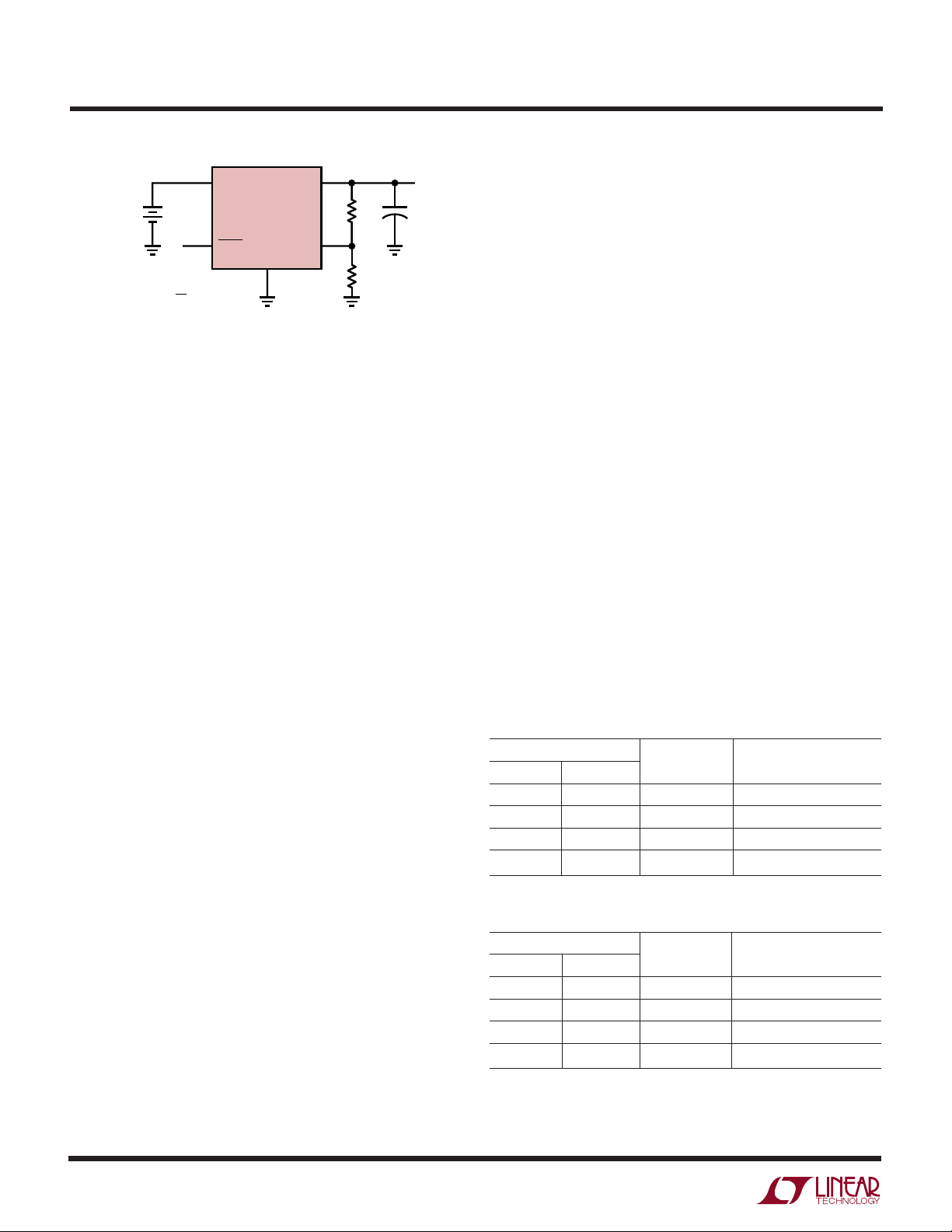
PIN FUNCTIONS
OUT (Pin 1): The output pin supplies power to the load. A
minimum output capacitor of 1.5µF is required to prevent
oscillations, but larger values of output capacitor will be
necessary to deal with larger load transients. See the
Applications Information section for more on output
capacitance and reverse output characteristics.
SENSE (Pin 2): For fixed voltage versions of the LT1521
(LT1521-3, LT1521-3.3, LT1521-5), the sense pin is the
input to the error amplifier. Optimum regulation will be
obtained at the point where the sense pin is connected to
300
200
(mA)
100
LOAD CURRENT
1.00.5 1.5 2.5 3.5 4.5
0
2.0
TIME (ms)
3.0
4.0
LT1521 • TPC34
5.0
the output pin of the regulator. In critical applications small
voltage drops caused by the resistance (RP) of PC traces
between the regulator and the load, which would normally
degrade regulation, may be eliminated by connecting the
sense pin to the output at the load as shown in Figure 1
(Kelvin Sense Connection). Note that the voltage drop
across the external PC traces will add to the dropout
voltage of the regulator. The sense pin bias current is 5µA
at the nominal regulated output voltage. This pin is internally clamped to –0.6V (one VBE).
1521335fb
8

UUU
PIN FUNCTIONS
5
IN
+
V
IN
4
SHDN
Figure 1. Kelvin Sense Connection
LT1521
GND
3
OUT
SENSE
LT1521/LT1521-3
LT1521-3.3/LT1521-5
R
P
1
+
2
R
P
LOAD
LT1521 • F01
VBE). This allows the shutdown pin to be driven directly by
5V logic or by open collector logic with a pull-up resistor.
The pull-up resistor is only required to supply the leakage
current of the open collector gate, normally several microamperes. Pull-up current must be limited to a maximum of
5mA. A curve of the shutdown pin input current as a
function of voltage appears in the Typical Performance
Characteristics. If the shutdown pin is not used it can be
left open circuit. The device will be active (output on) if the
shutdown pin is not connected.
ADJ (Pin 2): For adjustable LT1521, the adjust pin is the
input to the error amplifier. This pin is internally clamped
to 6V and –0.6V (one VBE). It has a bias current of 50nA
which flows into the pin. See Adjust Pin Bias Current vs
Temperature in the Typical Performance Characteristics
section. The adjust pin reference voltage is 3.75V referenced to ground. The output voltage range that can be
produced by this device is 3.75V to 20V.
SHDN (Pin 5): The shutdown pin is used to put the device
into shutdown. In shutdown the output of the device is
turned off. This pin is active low. The device will be shut
down if the shutdown pin is pulled low. The shutdown pin
current with the pin pulled to ground will be 1.7µA. The
shutdown pin is internally clamped to 7V and –0.6V (one
U
WUU
APPLICATIONS INFORMATION
The LT1521 is a 300mA low dropout regulator with
micropower quiescent current and shutdown. The device
is capable of supplying 300mA at a dropout of 0.5V and
operates with very low quiescent current (12µA). In shut-
down, the quiescent current drops to only 6µA. In addition
to the low quiescent current, the LT1521 incorporates
several protection features which make it ideal for use in
battery-powered systems. The device is protected against
both reverse input voltages and reverse output voltages.
In battery backup applications where the output can be
held up by a backup battery when the input is pulled to
ground, the LT1521 acts like it has a diode in series with
its output and prevents reverse current flow.
IN (Pin 8): Power is supplied to the device through the
input pin. The input pin should be bypassed to ground if
the device is more than six inches away from the main
input filter capacitor. In general, the output impedance of
battery rises with frequency, so it is advisable to include a
bypass capacitor in battery-powered circuits. A bypass
capacitor in the range of 1µF to 10µF is sufficient. The
LT1521 is designed to withstand reverse voltages on the
input pin with respect to ground and the output pin. In the
case of reversed input, which can happen if a battery is
plugged in backwards, the LT1521 will act as if there is a
diode in series with its input. There will be no reverse
current flow into the LT1521 and no reverse voltage will
appear at the load. The device will protect both itself and
the load.
Adjustable Operation
The adjustable version of the LT1521 has an output
voltage range of 3.75V to 20V. The output voltage is set by
the ratio of two external resistors as shown in Figure 2. The
device servos the output voltage to maintain the voltage at
the adjust pin at 3.75V. The current in R1 is then equal to
3.75V/R1. The current in R2 is equal to the sum of the
current in R1 and the adjust pin bias current. The adjust pin
bias current, 50nA at 25°C, flows through R2 into the
adjust pin. The output voltage can be calculated using the
formula in Figure 2. The value of R1 should be less than
400k to minimize errors in the output voltage caused by
the adjust pin bias current. Note that in shutdown the
1521335fb
9
LT1521/LT1521-3
LT1521-3.3/LT1521-5
U
WUU
APPLICATIONS INFORMATION
IN
V
IN
SHDN
V
= 3.75V 1 + + (I
OUT
= 3.75V
V
ADJ
= 50nA AT 25°C
I
ADJ
OUTPUT RANGE = 3.75V TO 20V
R2
)
R1
+ R2)
ADJ
)
LT1521
GND
OUT
R2
ADJ
R1
Figure 2. Adjustable Operation
output is turned off and the divider current will be zero.
Curves of Adjust Pin Voltage vs Temperature and Adjust
Pin Bias Current vs Temperature appear in the Typical
Performance Characteristics. The reference voltage at the
adjust pin has a positive temperature coefficient of approximately 15ppm/°C. The adjust pin bias current has a
negative temperature coefficient. These effects will tend to
cancel each other.
The adjustable device is specified with the adjust pin tied
to the output pin. This sets the output voltage to 3.75V.
Specifications for output voltages greater than 3.75V will
be proportional to the ratio of the desired output voltage
to 3.75V; (V
/3.75V). For example: load regulation for
OUT
an output current change of 1mA to 300mA is –20mV
typical at V
= 3.75V. At V
OUT
= 12V, load regulation
OUT
would be:
(12V/3.75V)(–20mV) = –64mV
Thermal Considerations
The power handling capability of the device will be limited
by the maximum rated junction temperature (125°C). The
power dissipated by the device will be made up of two
components:
1. Output current multiplied by the input/output voltage
differential: I
OUT(VIN
– V
OUT
), and
2. Ground pin current multiplied by the input voltage:
(I
)(VIN)
GND
V
OUT
+
LT1521 • F01
The ground pin current can be found by examining the
Ground Pin Current curves in the Typical Performance
Characteristics. Power dissipation will be equal to the sum
of the two components listed above.
The LT1521 series regulators have internal thermal limiting designed to protect the device during overload conditions. For continuous normal load conditions the maximum junction temperature rating of 125°C must not be
exceeded. It is important to give careful consideration to
all sources of thermal resistance from junction to ambient.
Additional heat sources mounted nearby must also be
considered.
For surface mount devices, heat sinking is accomplished
by using the heat spreading capabilities of the PC board
and its copper traces. Copper board stiffeners and plated
through-holes can also be used to spread the heat generated by power devices.
The following tables list thermal resistance for each package. Measured values of thermal resistance for several
different board sizes and copper areas are listed for each
package. All measurements were taken in still air on
3/32" FR-4 board with one ounce copper. All NC leads were
connected to the ground plane.
Table 1. MS8 Package
COPPER AREA
TOPSIDE** BACKSIDE BOARD AREA
2500mm22500mm
1000mm22500mm
225mm22500mm
100mm22500mm
* Pin 4 is ground. ** Device is mounted on topside.
2
2500mm
2
2500mm
2
2500mm
2
2500mm
Table 2. S8 Package*
COPPER AREA
TOPSIDE** BACKSIDE BOARD AREA
2500mm22500mm
1000mm22500mm
225mm22500mm
100mm22500mm
* Pins 3, 6, 7 are ground. ** Device is mounted on topside.
2
2500mm
2
2500mm
2
2500mm
2
2500mm
THERMAL RESISTANCE
(JUNCTION-TO-AMBIENT)
2
2
2
2
2
2
2
2
110°C/W
115°C/W
120°C/W
130°C/W
THERMAL RESISTANCE
(JUNCTION-TO-AMBIENT)
60°C/W
60°C/W
68°C/W
74°C/W
10
1521335fb
LT1521/LT1521-3
LT1521-3.3/LT1521-5
U
WUU
APPLICATIONS INFORMATION
Table 3. SOT-223 Package
(Thermal Resistance Junction-to-Tab 20°C/W)
COPPER AREA
TOPSIDE* BACKSIDE BOARD AREA
2500mm22500mm
1000mm22500mm
2
225mm
100mm
1000mm21000mm
1000mm
* Tab of device attached to topside copper.
2
2
2500mm
2500mm
2
2500mm
2
2500mm
2
2500mm
2
2500mm
2
1000mm
0 1000mm
Calculating Junction Temperature
Example: Given an output voltage of 3.3V, an input voltage
range of 4.5V to 7V, an output current range of 0mA to
150mA and a maximum ambient temperature of 50°C,
what will the maximum junction temperature be?
The power dissipated by the device will be equal to:
I
OUT(MAX)(VIN(MAX)
– V
OUT
) + I
Where,
I
OUT(MAX)
V
IN(MAX)
I
GND
at (I
= 150mA
= 7V
= 150mA, VIN = 7V) = 2.1mA
OUT
So,
P = 150mA(7V – 3.3V) + (2.1mA)(7V) = 0.57W
If we use a SOT-223 package, then the thermal resistance
will be in the range of 50°C/W to 65°C/W depending on the
copper area. So the junction temperature rise above
ambient will be approximately equal to:
0.57W(60°C/W) = 34.2°C
The maximum junction temperature will then be equal to the
maximum junction temperature rise above ambient plus the
maximum ambient temperature or:
T
= 50°C + 34.2°C = 84.2°C
JMAX
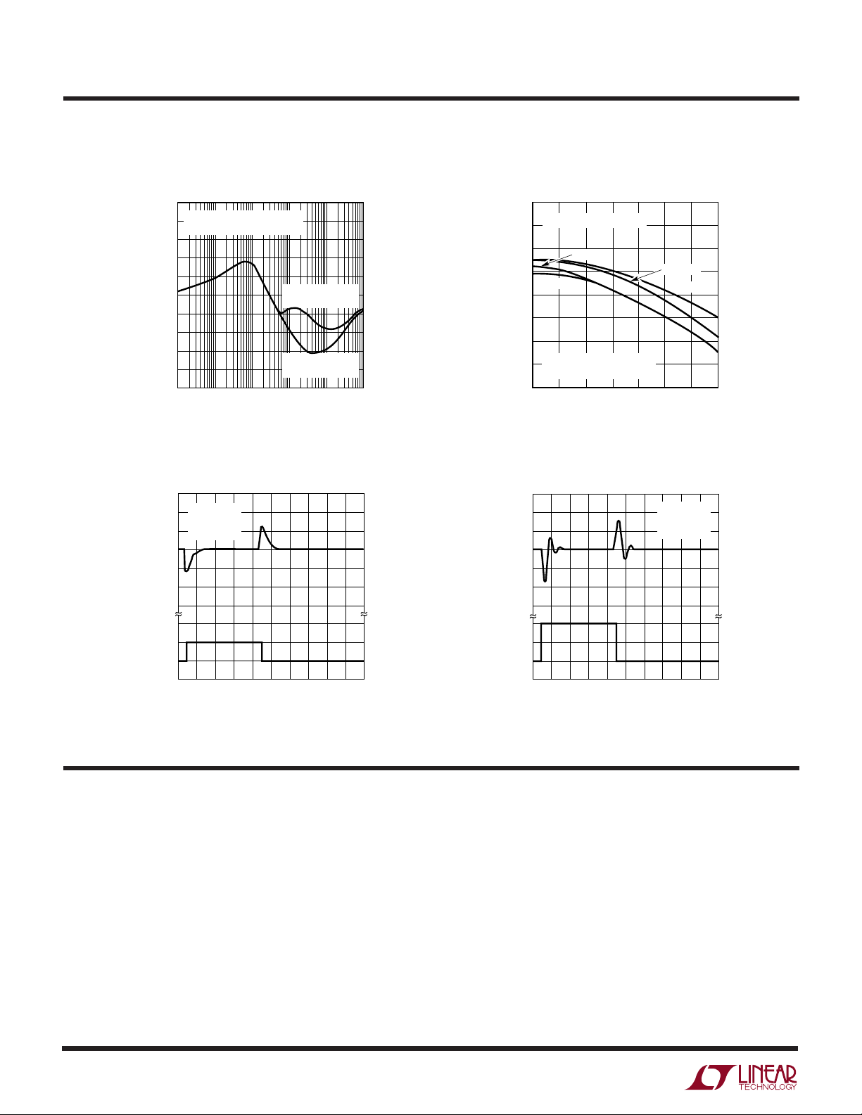
Output Capacitance and Transient Performance
The LT1521 is designed to be stable with a wide range of
output capacitors. A minimum output capacitor of 1.5µF
THERMAL RESISTANCE
(JUNCTION-TO-AMBIENT)
2
2
2
2
2
2
GND(VIN(MAX)
50°C/W
50°C/W
58°C/W
64°C/W
57°C/W
60°C/W
)
is required to prevent oscillations. The LT1521 is a
micropower device and output transient response will be
a function of output capacitance. See the Transient
Response curves in the Typical Performance Characteristics. Larger values of output capacitance will decrease the
peak deviations and provide improved output transient
response for larger load current deltas. Bypass capacitors, used to decouple individual components powered by
the LT1521, will increase the effective value of the output
capacitor.
Protection Features
The LT1521 incorporates several protection features which
make it ideal for use in battery-powered circuits. In
addition to the normal protection features associated with
monolithic regulators, such as current limiting and thermal limiting, the device is protected against reverse input
voltages, reverse output voltages and reverse voltages
from output to input.
Current limit protection and thermal overload protection
are intended to protect the device against current overload
conditions at the output of the device. For normal operation, the junction temperatures should not exceed 125°C.
The input of the device will withstand reverse voltages of
20V. Current flow into the device will be limited to less
than 1mA (typically less than 100µA) and no negative
voltage will appear at the output. The device will protect
both itself and the load. This provides protection against
batteries that can be plugged in backward.
For fixed voltage versions of the device, the output can be
pulled below ground without damaging the device. If the
input is left open circuit or grounded, the output can be
pulled below ground by 20V. The output will act like an
open circuit, no current will flow out of the pin. If the input
is powered by voltage source, the output will source the
short-circuit current of the device and will protect itself by
thermal limiting. For the adjustable version of the device,
the output pin is internally clamped at one diode drop
below ground. Reverse current for the adjustable device
must be limited to 5mA.
1521335fb
11
LT1521/LT1521-3
LT1521-3.3/LT1521-5
U
WUU
APPLICATIONS INFORMATION
In circuits where a backup battery is required, several
different input/output conditions can occur. The output
voltage may be held up while the input is either pulled to
ground, pulled to some intermediate voltage or is left open
circuit. Current flow back into the output will vary depending on the conditions. Many battery-powered circuits
incorporate some form of power management. The following information will help optimize battery life. Table 4
summarizes the following information.
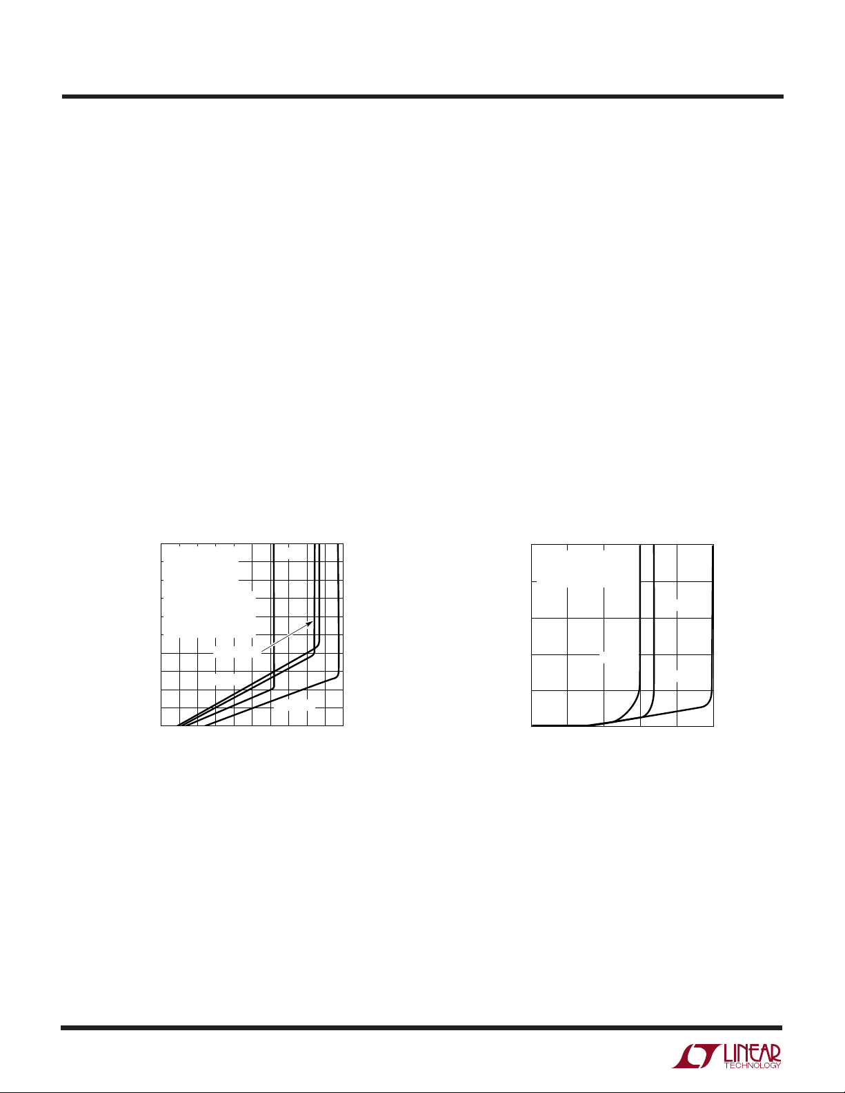
The reverse output current will follow the curve in Figure
3 when the input is pulled to ground. This current flows
through the output pin to ground. The state of the shutdown pin will have no effect on output current when the
input pin is pulled to ground.
In some applications it may be necessary to leave the input
on the LT1521 unconnected when the output is held high.
This can happen when the LT1521 is powered from a
rectified AC source. If the AC source is removed, then the
input of the LT1521 is effectively left floating. The reverse
output current also follows the curve in Figure 3 if the input
pin is left open. The state of the shutdown pin will have no
effect on the reverse output current when the input pin is
floating.
When the input of the LT1521 is forced to a voltage below
its nominal output voltage and its output is held high, the
output current will follow the curve shown in Figure 3. This
can happen if the input of the LT1521 is connected to a
discharged (low voltage) battery and the output is held up
by either a backup battery or by second regulator circuit.
When the input pin is forced below the output pin or the
output pin is pulled above the input pin, the input current
will typically drop to less than 2µA (see Figure 4). The state
of the shutdown pin will have no effect on the reverse
output current when the output is pulled above the input.
50
TJ = 25°C
45
V
IN
CURRENT FLOWS
40
INTO OUTPUT PIN
V
OUT
35
(LT1521-3/LT1521-3.3
30
LT1521-5)
V
OUT
25
20
15
10
REVERSE OUTPUT CURRENT (µA)
5
0
0
= 0V
= V
SENSE
= V
(LT1521)
ADJ
LT1521-3.3
LT1521-3
3579
21
4
OUTPUT VOLTAGE (V)
LT1521
LT1521-5
6
Figure 3. Reverse Output Current
8
LT1521 • F03
5
V
= 3V (LT1521-3)
OUT
= 3.3V (LT1521-3.3)
V
OUT
= 5V (LT1521-5)
V
OUT
4
3
LT1521-3.3
LT1521-5
4
LT1521 • F04
5
3
2
INPUT CURRENT (µA)
1
10
0
0
LT1521-3
1
2
INPUT VOLTAGE (V)
Figure 4. Input Current
12
1521335fb
LT1521/LT1521-3
LT1521-3.3/LT1521-5
U
WUU
APPLICATIONS INFORMATION
Table 4. Fault Conditions
INPUT PIN SHDN PIN OUTPUT/SENSE PINS RESULTING CONDITIONS
< V
(Nominal) Open (High) Forced to V
OUT
< V
(Nominal) Grounded Forced to V
OUT
Open Open (High) > 1V Reverse Output Current ≈ 5µA (See Figure 3)
Open Grounded > 1V Reverse Output Current ≈ 5µA (See Figure 3)
≤ 0.8V Open (High) ≤ 0V Output Current = 0
≤ 0.8V Grounded ≤ 0V Output Current = 0
> 1.5V Open (High) ≤ 0V Output Current = Short-Circuit Current
–20V < VIN < 20V Grounded ≤ 0V Output Current = 0
(Nominal) Reverse Output Current ≈ 5µA (See Figure 3)
OUT
Input Current ≈ 1µA (See Figure 4)
(Nominal) Reverse Output Current ≈ 5µA (See Figure 3)
OUT
Input Current ≈ 1µA (See Figure 4)
U
PACKAGE DESCRIPTION
MS8 Package
8-Lead Plastic MSOP
(Reference LTC DWG # 05-08-1660)
0.889
± 0.127
(.035 ± .005)
5.23
(.206)
MIN
0.42 ± 0.04
(.0165 ± .0015)
TYP
RECOMMENDED SOLDER PAD LAYOUT
0.254
(.010)
GAUGE PLANE
0.18
(.077)
NOTE:
1. DIMENSIONS IN MILLIMETER/(INCH)
2. DRAWING NOT TO SCALE
3. DIMENSION DOES NOT INCLUDE MOLD FLASH, PROTRUSIONS OR GATE BURRS.
MOLD FLASH, PROTRUSIONS OR GATE BURRS SHALL NOT EXCEED 0.152mm (.006") PER SIDE
4. DIMENSION DOES NOT INCLUDE INTERLEAD FLASH OR PROTRUSIONS.
INTERLEAD FLASH OR PROTRUSIONS SHALL NOT EXCEED 0.152mm (.006") PER SIDE
5. LEAD COPLANARITY (BOTTOM OF LEADS AFTER FORMING) SHALL BE 0.102mm (.004") MAX
DETAIL “A”
(.126 – .136)
(.0256)
° – 6° TYP
0
DETAIL “A”
3.2 – 3.45
0.65
BSC
0.53 ± 0.015
(.021 ± .006)
SEATING
PLANE
3.00 ± 0.102
(.118 ± .004)
(NOTE 3)
4.88
± 0.1
(.192 ± .004)
(.043)
0.22 – 0.38
(.009 – .015)
1.10
MAX
8
12
0.65
(.0256)
BCS
7
0.52
5
4
(.206)
REF
3.00 ± 0.102
(.118 ± .004)
NOTE 4
0.86
(.034)
REF
0.13 ± 0.05
(.005 ± .002)
MSOP (MS8) 1001
1521335fb
6
3
13

LT1521/LT1521-3
LT1521-3.3/LT1521-5
PACKAGE DESCRIPTION
U
S8 Package
8-Lead Plastic Small Outline (Narrow .150 Inch)
(Reference LTC DWG # 05-08-1610)
0.189 – 0.197*
(4.801 – 5.004)
7
8
6
5
0.228 – 0.244
(5.791 – 6.197)
0.010 – 0.020
(0.254 – 0.508)
0.008 – 0.010
(0.203 – 0.254)
*
DIMENSION DOES NOT INCLUDE MOLD FLASH. MOLD FLASH
SHALL NOT EXCEED 0.006" (0.152mm) PER SIDE
**
DIMENSION DOES NOT INCLUDE INTERLEAD FLASH. INTERLEAD
FLASH SHALL NOT EXCEED 0.010" (0.254mm) PER SIDE
×
°
45
0.016 – 0.050
(0.406 – 1.270)
0°– 8° TYP
0.053 – 0.069
(1.346 – 1.752)
0.014 – 0.019
(0.355 – 0.483)
TYP
0.150 – 0.157**
(3.810 – 3.988)
1
3
2
4
0.004 – 0.010
(0.101 – 0.254)
0.050
(1.270)
BSC
SO8 1298
14
1521335fb

PACKAGE DESCRIPTION
0.248 – 0.264
(6.30 – 6.71)
0.114 – 0.124
(2.90 – 3.15)
0.264 – 0.287
(6.70 – 7.30)
0.130 – 0.146
(3.30 – 3.71)
LT1521/LT1521-3
LT1521-3.3/LT1521-5
U
ST Package
3-Lead Plastic SOT-223
(Reference LTC DWG # 05-08-1630)
0.071
(1.80)
MAX
0.0905
(2.30)
NOM
0.024 – 0.033
(0.60 – 0.84)
0.181
(4.60)
NOM
0.033 – 0.041
(0.84 – 1.04)
0.012
(0.31)
MIN
10°
MAX
10° – 16°
0.010 – 0.014
(0.25 – 0.36)
10° – 16°
0.0008 – 0.0040
(0.0203 – 0.1016)
ST3 (SOT-233) 1298
Information furnished by Linear Technology Corporation is believed to be accurate and reliable.
However, no responsibility is assumed for its use. Linear Technology Corporation makes no representation that the interconnection of its circuits as described herein will not infringe on existing patent rights.
1521335fb
15

LT1521/LT1521-3
LT1521-3.3/LT1521-5
RELATED PARTS
PART NUMBER DESCRIPTION COMMENTS
LTC®1174 425mA High Efficiency Step-Down Switching Regulator >90% Efficiency, SO-8 Package
LT1175 500mA Micropower Low Dropout Negative Linear Regulator Selectable Current Limit
LT1120A 125mA Micropower Low Dropout Linear Regulator 20µA Quiescent Current, Includes Comparator
LT1304 Micropower Step-Up DC/DC Converter 15µA Quiescent Current, 1.5 Minimum Input
LT1529 3A Micropower Low Dropout Regulator 50µA Quiescent Current
LT1761 100mA Low Noise Micropower Low Dropout Regulator IQ = 30µA, Low Noise 20µV
LT1762 150mA Low Noise Micropower Low Dropout Regulator IQ = 30µA, Low Noise 20µV
LT1763 500mA Low Noise Micropower Low Dropout Regulator IQ = 30µA, Low Noise 20µV
LT1962 300mA Low Noise Micropower Low Dropout Regulator IQ = 30µA, Low Noise 20µV
ThinSOT is a registered trademark of Linear Technology Corporation.
, VIN = 1.8V to 20V, ThinSOT
RMS
, VIN = 1.8V to 20V, MSOP-8
RMS
, VIN = 1.8V to 20V, SO-8
RMS
, VIN = 1.8V to 20V, MSOP-8
RMS
®
16
Linear Technology Corporation
1630 McCarthy Blvd., Milpitas, CA 95035-7417
(408) 432-1900 ● FAX: (408) 434-0507
●
www.linear.com
1521335fb
LT/CPI 0302 REV B 1.5K • PRINTED IN USA
LINEAR TECHNOLOGY CORPORATION 1995
 Loading...