

Page 1
LT1206
250mA/60MHz Current
Feedback Amplifi er
FEATURES
■
250mA Minimum Output Drive Current
■
60MHz Bandwidth, AV = 2, RL = 100Ω
■
900V/µs Slew Rate, AV = 2, RL = 50Ω
■
0.02% Differential Gain, AV = 2, RL = 30Ω
■
0.17° Differential Phase, AV = 2, RL = 30Ω
■
High Input Impedance, 10MΩ
■
Wide Supply Range, ±5V to ±15V
■
Shutdown Mode: IS < 200µA
■
Adjustable Supply Current
■
Stable with CL = 10,000p
■
Available in 8-Pin DIP and SO and 7-Pin DD and
TO-220 Packages
APPLICATIONS
■
Video Amplifi ers
■
Cable Drivers
■
RGB Amplifi ers
■
Test Equipment Amplifi ers
■
Buffers
DESCRIPTION
The LT®1206 is a current feedback amplifi er with high
output current drive capability and excellent video characteristics. The LT1206 is stable with large capacitive
loads, and can easily supply the large currents required
by the capacitive loading. A shutdown feature switches
the device into a high impedance, low current mode,
reducing dissipation when the device is not in use. For
lower bandwidth applications, the supply current can be
reduced with a single external resistor. The low differential
gain and phase, wide bandwidth, and the 250mA minimum output current drive make the LT1206 well suited
to drive multiple cables in video systems.
The LT1206 is manufactured on Linear Technology’s
proprietary complementary bipolar process.
, LT, LTC and LTM are registered trademarks of Linear Technology Corporation.
All other trademarks are the property of their respective owners.
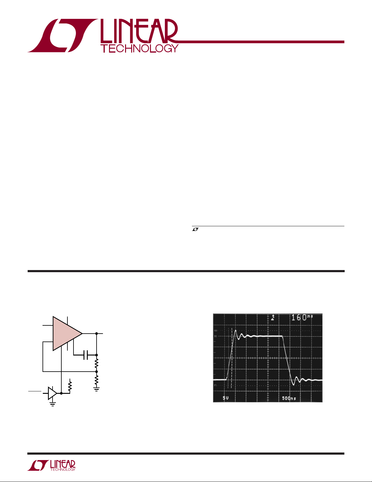
TYPICAL APPLICATION
Noninverting Amplifi er with Shutdown
15V
V
ENABLE
+
IN
V
OUT
R
F
OPTIONAL, USE WITH CAPACITIVE LOADS
*
R
G
GROUND SHUTDOWN PIN FOR
**
NORMAL OPERATION
5V
LT1206
S/D**
–
74C906
LT1206 • TA01
–15V
15V
COMP
24k
C
COMP
0.01µF*
Large-Signal Response, CL = 10,000pF
= ±15V
V
S
= RG = 3k
R
L
= ∞
R
L
500ns/DIV
1206 TA02
1206fa
1
Page 2

LT1206
ABSOLUTE MAXIMUM RATINGS
(Note 1)
Supply Voltage ........................................................±18V
Input Current ........................................................±15mA
Output Short-Circuit Duration (Note 2) .........Continuous
Specifi ed Temperature Range (Note 3) ........0°C to 70°C
PACKAGE/OERDER INFORMATION
TOP VIEW
NC
1
–IN
2
+IN
3
S/D*
4
N8 PACKAGE
8-LEAD PLASTIC DIP
θJA = 100°C/W
ORDER PART NUMBER ORDER PART NUMBER S8 PART MARKING
LT1206CN8** LT1206CS8** 1206
FRONT VIEW
7
6
5
4
3
TAB IS
+
V
R PACKAGE
7-LEAD PLASTIC DD
2
1
θJA = 30°C/W
+
V
8
OUT
7
–
V
6
COMP
5
OUT
–
V
COMP
+
V
S/D*
+IN
–IN
Operating Temperature Range ................. –40°C to 85°C
Junction Temperature ........................................... 150°C
Storage Temperature Range ................... –65°C to 150°C
Lead Temperature (Soldering, 10 sec) ..................300°C
TOP VIEW
+
8
V
OUT
7
–
V
6
COMP
5
OUT
–
V
COMP
+
V
S/D*
+IN
–IN
TAB IS
+
V
+
V
1
–IN
2
+IN
3
S/D*
4
S8 PACKAGE
8-LEAD PLASTIC SO
θJA = 60°C/W
FRONT VIEW
T7 PACKAGE
7-LEAD PLASTIC TO-220
θJA = 5°C/W
7
6
5
4
3
2
1
ORDER PART NUMBER ORDER PART NUMBER
LT1206CR** LT1206CT7**
Order Options Tape and Reel: Add #TR
Lead Free: Add #PBF Lead Free Tape and Reel: Add #TRPBF
Lead Free Part Marking: http://www.linear.com/leadfree/
Consult LTC Marketing for parts specifi ed with wider operating temperature ranges. *Ground shutdown pin for normal operation. ** See Note 3.
ELECTRICAL CHARACTERISTICS
The
temperature range, otherwise specifi cations are at T
= 25°C. VCM = 0, ±5V ≤ VS ≤ 15V, pulse tested, V
A
●
denotes the specifi cations which apply over the full operating
= 0V, unless otherwise noted.
S/D
SYMBOL PARAMETER CONDITIONS MIN TYP MAX UNITS
V
OS
+
I
IN
–
I
IN
Input Offset Voltage
Input Offset Voltage Drift
Noninverting Input Current
Inverting Input Current
●
●
●
●
±3 ±10
±15
mV
mV
10 µV/°C
±2 ±8
±25
±10 ±60
±100
1206fa
µA
µA
µA
µA
2
Page 3

LT1206
ELECTRICAL CHARACTERISTICS
The
temperature range, otherwise specifi cations are at T
SYMBOL PARAMETER CONDITIONS MIN TYP MAX UNITS
e
n
+i
n
–i
n
R
IN
C
IN
CMRR Common Mode Rejection Ratio V
PSRR Power Supply Rejection Ratio V
A
V
R
OL
V
OUT
I
OUT
I
S
SR Slew Rate (Note 5) A
BW Small-Signal Bandwidth V
Note 1: Stresses beyond those listed under Absolute Maximum Ratings
may cause permanent damage to the device. Exposure to any Absolute
Maximum Rating condition for extended periods may affect device
reliability and lifetime.
Note 2: Applies to short circuits to ground only. A short circuit between
the output and either supply may permanently damage the part when
operated on supplies greater than ±10V.
Input Noise Voltage Density f = 10kHz, RF = 1k, RG = 10Ω, RS = 0Ω 3.6 nV/√Hz
Input Noise Current Density f = 10kHz, RF = 1k, RG = 10Ω, RS = 10k 2 pA/√Hz
Input Noise Current Density f = 10kHz, RF = 1k, RG = 10Ω, RS = 10k 30 pA/√Hz
Input Resistance VIN = ±12V, VS = ±15V
Input Capacitance VS = ±15V 2 pF
Input Voltage Range V
Inverting Input Current Common Mode
Rejection
Noninverting Input Current Power Supply
Rejection
Inverting Input Current Power Supply
Rejection
Large-Signal Voltage Gain VS = ±15V, V
Transresistance, ΔV
OUT
/ΔI
–
IN
Maximum Output Voltage Swing VS = ±15V, RL = 50Ω
Maximum Output Current RL = 1Ω
Supply Current VS = ±15V, V
Supply Current, R
= 51k (Note 4) VS = ±15V 12 17 mA
S/D
Positive Supply Current, Shutdown V
Output Leakage Current, Shutdown V
Differential Gain (Note 6) V
Differential Phase (Note 6) V
= 25°C. VCM = 0, ±5V ≤ VS ≤ 15V, pulse tested, V
A
V
= ±2V, VS = ±5V
IN
= ±15V
S
V
= ±5V
S
= ±15V, VCM = ±12V
S
V
= ±5V, VCM = ±2V
S
= ±15V, VCM = ±12V
V
S
V
= ±5V, VCM = ±2V
S
= ±5V to ±15V
S
= ±5V to ±15V
V
S
= ±5V to ±15V
V
S
V
= ±5V, V
S
VS = ±15V, V
V
= ±5V, V
S
= ±15V, RL = 25Ω
V
S
= ±15V, V
S
= ±15V, V
S
= 2 400 900 V/µs
V
= ±15V, RF = 560Ω, RG = 560Ω, RL = 30Ω 0.02 %
S
= ±15V, RF = 560Ω, RG = 560Ω, RL = 30Ω 0.17 Deg
S
= ±15V, Peaking ≤ 0.5dB,
S
R
= RG = 620Ω, RL = 100Ω
F
= ±15V, Peaking ≤ 0.5dB,
V
S
R
= RG = 649Ω, RL = 50Ω
F
= ±15V, Peaking ≤ 0.5dB,
V
S
R
= RG = 698Ω, RL = 30Ω
F
= ±15V, Peaking ≤ 0.5dB,
V
S
= RG = 825Ω, RL = 10Ω
R
F
●
denotes the specifi cations which apply over the full operating
= 0V, unless otherwise noted.
S/D
●
= ±10V, RL = 50Ω
OUT
= ±2V, RL = 25Ω
OUT
= ±10V, RL = 50Ω
OUT
= ±2V, RL = 25Ω
OUT
= 0V
S/D
= 15V
S/D
= 15V
S/D
1.5
●
0.5
●
±12±2±13.5
●
●
55
●
50
●
●
●
60 77 dB
●
●
●
55
●
55
●
100
●
75
±11.5
●
±10.0
±2.5
●
±2.0
●
250 500 1200 mA
●
●
●
10
5
±3.5
62
60
0.1
0.1
30 500 nA/V
0.7 5 µA/V
71
68
260
200
±12.5 V
±3.0 V
20 30
60 MHz
52 MHz
43 MHz
27 MHz
Note 3: Commercial grade parts are designed to operate over the
temperature range of –40°C to 85°C but are neither tested nor guaranteed
beyond 0°C to 70°C. Industrial grade parts tested over –40°C to 85°C are
available on special request. Consult factory.
Note 4: R
is connected between the shutdown pin and ground.
S/D
Note 5: Slew rate is measured at ±5V on a ±10V output signal while
operating on ±15V supplies with R
= 1.5k, RG = 1.5k and RL = 400Ω.
F
Note 6: NTSC composite video with an output level of 2V.
MΩ
MΩ
10
10
µA/V
µA/V
kΩ
kΩ
mA
35
mA
200 µA
10 µA
1206fa
V
V
dB
dB
dB
dB
V
V
3
Page 4

LT1206
SMALL-SIGNAL BANDWIDTH
IS = 20mA Typical, Peaking ≤ 0.1dB
–3dB BW
(MHz)
48
34
22
54
36
22.4
48
35
22.4
40
31
20
–3dB BW
(MHz)
35
25
16.4
37
25
16.5
35
25
16.2
31
23
15
S/D
R
L
= 0Ω
A
V
= ±5V, R
S
V
–1 150
30
10
1 150
30
10
2 150
30
10
10 150
30
10
I
= 10mA Typical, Peaking ≤ 0.1dB
S
A
V
VS = ±5V, R
R
= 10.2k
S/D
L
–1 150
30
10
1 150
30
10
2 150
30
10
10 150
30
10
R
562
649
732
619
715
806
576
649
750
442
511
649
R
576
681
750
665
768
845
590
681
768
301
392
499
F
F
R
G
562
649
732
–
–
–
576
649
750
48.7
56.2
71.5
R
G
576
681
750
–
–
–
590
681
768
33.2
43.2
54.9
–0.1dB BW
(MHz)
21.4
17
12.5
22.3
17.5
11.5
20.7
18.1
11.7
19.2
16.5
10.2
–0.1dB BW
(MHz)
17
12.5
8.7
17.5
12.6
8.2
16.8
13.4
8.1
15.6
11.9
7.8
A
V
V
= ±15V, R
S
–1 150
1 150
2 150
10 150
A
V
VS = ±15V, R
–1 150
1 150
2 150
10 150
R
= 0Ω
S/D
30
10
30
10
30
10
30
10
R
= 60.4k
S/D
30
10
30
10
30
10
30
10
–3dB BW
L
R
F
681
768
887
768
909
1k
665
787
931
487
590
768
R
681
768
887
–
–
–
665
787
931
536
64.9
84.5
G
(MHz)
50
35
24
66
37
23
55
36
22.5
44
33
20.7
–3dB BW
L
R
F
634
768
866
768
909
1k
649
787
931
301
402
590
R
634
768
866
–
–
–
649
787
931
33.2
44.2
64.9
G
(MHz)
41
26.5
17
44
28
16.8
40
27
16.5
33
25
15.3
–0.1dB BW
(MHz)
19.2
17
12.3
22.4
17.5
12
23
18.5
11.8
20.7
17.5
10.8
–0.1dB BW
(MHz)
19.1
14
9.4
18.8
14.4
8.3
18.5
14.1
8.1
15.6
13.3
7.4
I
= 5mA Typical, Peaking ≤ 0.1dB
S
A
V
VS = ±5V, R
–1 150
1 150
2 150
10 150
R
= 22.1k
S/D
30
10
30
10
30
10
30
10
L
R
F
604
715
681
768
866
825
634
750
732
100
100
100
4
R
G
604
715
681
–
–
–
634
750
732
11.1
11.1
11.1
–3dB BW
(MHz)
21
14.6
10.5
20
14.1
9.8
20
14.1
9.6
16.2
13.4
9.5
–0.1dB BW
(MHz)
10.5
7.4
6.0
9.6
6.7
5.1
9.6
7.2
5.1
5.8
7.0
4.7
A
V
VS = ±15V, R
–1 150
1 150
2 150
10 150
R
S/D
30
10
30
10
30
10
30
10
L
= 121k
R
619
787
825
845
1k
1k
681
845
866
100
100
100
–3dB BW
F
R
G
619
787
825
–
–
–
681
845
866
11.1
11.1
11.1
(MHz)
25
15.8
10.5
23
15.3
10
23
15
10
15.9
13.6
9.6
–0.1dB BW
(MHz)
12.5
8.5
5.4
10.6
7.6
5.2
10.2
7.7
5.4
4.5
6
4.5
1206fa
Page 5
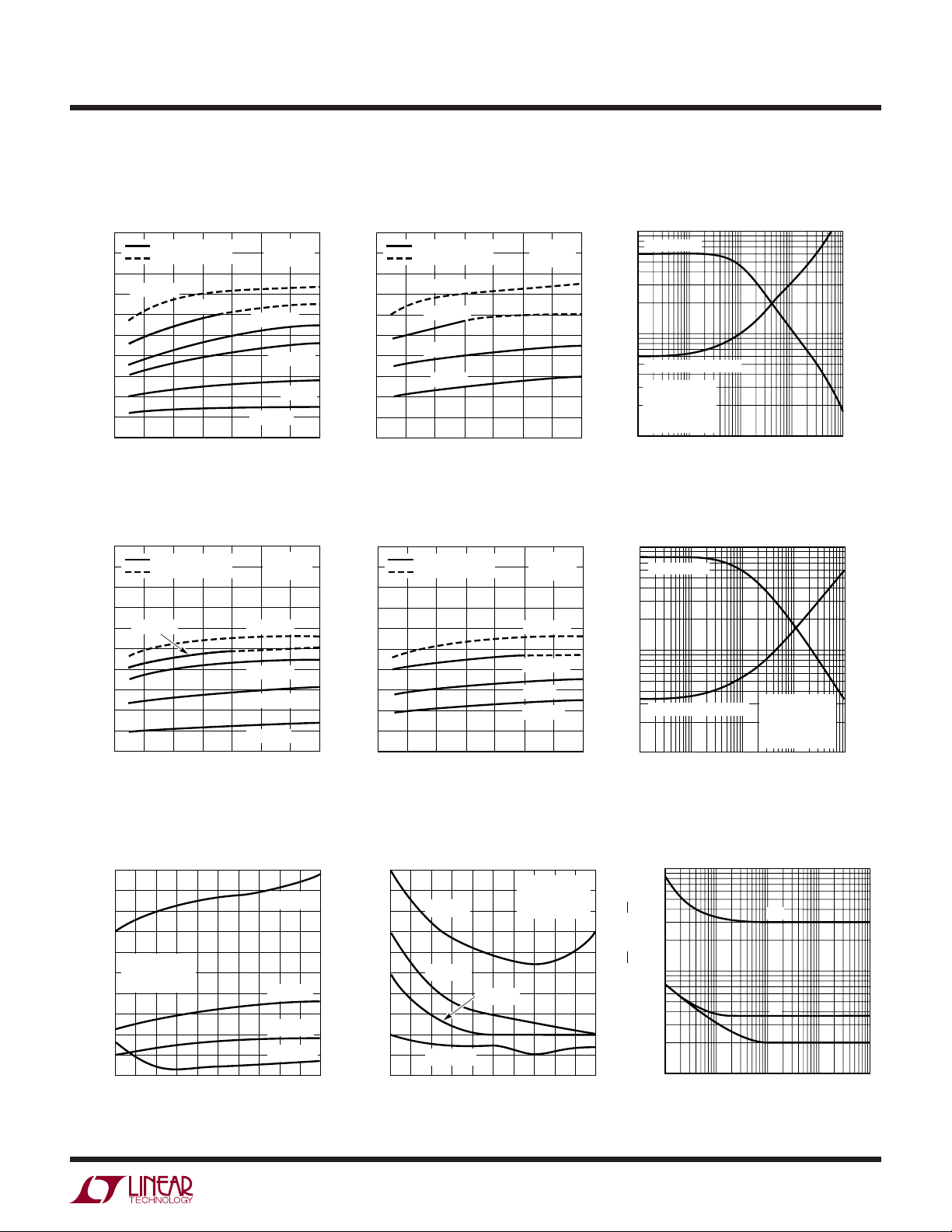
TYPICAL PERFORMANCE CHARACTERISTICS
Bandwidth vs Supply Voltage
100
90
80
70
60
50
40
30
– 3dB BANDWIDTH (MHz)
20
10
0
PEAKING ≤ 0.5dB
PEAKING ≤ 5dB
RF = 470Ω
RF = 560Ω
4
610
8
SUPPLY VOLTAGE (±V)
Bandwidth vs Supply Voltage
100
90
80
70
60
50
40
30
–3dB BANDWIDTH (MHz)
20
10
0
PEAKING ≤ 0.5dB
PEAKING ≤ 5dB
RF =390Ω
4
610
8
SUPPLY VOLTAGE (±V)
12
12
AV = 2
= 100Ω
R
L
RF = 680Ω
RF = 750Ω
RF = 1.5k
14
LT1206 • TPC01
AV = 10
= 100Ω
R
L
RF = 330Ω
RF = 470Ω
RF = 680Ω
RF = 1.5k
14
LT1206 • TPC04
RF = 1k
16
16
18
18
Bandwidth vs Supply Voltage
50
40
30
20
–3dB BANDWIDTH (MHz)
10
0
PEAKING ≤ 0.5dB
PEAKING ≤ 5dB
RF = 560Ω
RF = 750Ω
RF = 1k
RF = 2k
4
610
8
SUPPLY VOLTAGE (±V)
Bandwidth vs Supply Voltage
50
40
30
20
– 3dB BANDWIDTH (MHz)
10
0
PEAKING ≤ 0.5dB
PEAKING ≤ 5dB
4
610
8
SUPPLY VOLTAGE (±V)
AV = 2
R
L
14
12
LT1206 • TPC02
AV = 10
R
L
RF = 560Ω
RF = 680Ω
RF = 1k
RF = 1.5k
14
12
LT1206 • TPC05
= 10Ω
16
= 10Ω
16
LT1206
Bandwidth and Feedback Resistance
vs Capacitive Load for 0.5dB Peak
10k
BANDWIDTH
1k
FEEDBACK RESISTOR
FEEDBACK RESISTOR (Ω)
18
100
= 2
A
V
= ∞
R
L
= ±15V
V
S
= 0.01µF
C
COMP
100 10000
1
10 1000
CAPACITIVE LOAD (pF)
LT1206 • TPC03
Bandwidth and Feedback Resistance
vs Capacitive Load for 5dB Peak
10k
BANDWIDTH
1k
FEEDBACK RESISTOR (Ω)
FEEDBACK RESISTOR
0100
18
0
1
10 100 1k 10k
CAPACITIVE LOAD (pF)
AV = +2
= ∞
R
L
= ±15V
V
S
C
COMP
= 0.01µF
LT1206 • TPC06
100
–3dB BANDWIDTH (MHz)
10
1
100
–3dB BANDWIDTH (MHz)
10
1
Differential Phase
vs Supply Voltage
0.50
0.40
0.30
RF = RG = 560Ω
= 2
A
V
N PACKAGE
0.20
DIFFERENTIAL PHASE (DEG)
0.10
0
7
5
9
SUPPLY VOLTAGE (±V)
Differential Gain
vs Supply Voltage
0.10
RL = 15Ω
RL = 30Ω
RL = 50Ω
RL = 150Ω
11
13
15
LT1206 • TPC07
0.08
0.06
0.04
DIFFERENTIAL GAIN (%)
0.02
0
RL = 15Ω
RL = 30Ω
RL = 150Ω
7
5
9
SUPPLY VOLTAGE (±V)
RL = 50Ω
RF = RG = 560Ω
= 2
A
V
N PACKAGE
11
13
LT1206 • TPC08
15
Spot Noise Voltage and Current
vs Frequency
100
–i
n
10
e
n
i
SPOT NOISE (nV/√Hz OR pA/√Hz)
1
10
100 100k
n
1k 10k
FREQUENCY (Hz)
LT1206 • TPC09
1206fa
5
Page 6

LT1206
TYPICAL PERFORMANCE CHARACTERISTICS
Supply Current vs Supply Voltage
24
V
= 0V
S/D
22
20
18
16
14
SUPPLY CURRENT (mA)
12
10
4
610
TJ = –40˚C
TJ = 25˚C
TJ = 85˚C
TJ = 125˚C
8
SUPPLY VOLTAGE (±V)
12
Supply Current vs Shutdown Pin
Current
20
VS = ±15V
18
16
14
12
10
8
6
SUPPLY CURRENT (mA)
4
2
0
100
0
SHUTDOWN PIN CURRENT (µA)
200
300
14
LT1206 • TPC10
400
16
LT1206 • TPC13
25
20
15
10
SUPPLY CURRENT (mA)
18
+
V
– 0.5
–1.0
–1.5
–2.0
2.0
1.5
1.0
COMMON-MODE RANGE (V)
0.5
–
500
V
Supply Current vs Ambient
Temperature, V
RSD = 0Ω
RSD = 10.2k
R
5
0
–50
SD
–25
= ±5V
S
= 22.1k
50
25
0
TEMPERATURE (°C)
AV = 1
R
L
N PACKAGE
75
Input Common Mode Limit vs
Junction Temperature
–25 100
–50
0 125
25
TEMPERATURE (°C)
75
50
= ∞
100
LT1206 • TPC11
LT1206 • TPC14
125
Supply Current vs Ambient
Temperature, VS = ±15V
25
RSD = 0Ω
20
15
–25
0
RSD = 60.4k
R
= 121k
SD
50
25
TEMPERATURE (°C)
10
SUPPLY CURRENT (mA)
5
0
–50
Output Short-Circuit Current vs
Junction Temperature
1.0
0.9
0.8
0.7
0.6
0.5
0.4
OUTPUT SHORT-CIRCUIT CURRENT (A)
0.3
–50
–25 0
SOURCING
SINKING
50 100 125
25 75
TEMPERATURE (°C)
AV = 1
= ∞
R
L
N PACKAGE
75
100
LT1206 • TPC12
LT1206 • TPC15
125
Output Saturation Voltage vs
Junction Temperature
+
V
VS = ±15V
–1
–2
–3
–4
4
3
2
OUTPUT SATURATION VOLTAGE (V)
1
–
V
–25 100
–50
0 125
25
TEMPERATURE (°C)
6
50
RL = 2k
RL = 50Ω
RL = 50Ω
RL = 2k
75
LT1206 • TPC16
Power Supply Rejection Ratio vs
Frequency
70
60
NEGATIVE
50
POSITIVE
40
30
20
POWER SUPPLY REJECTION (dB)
10
0
10k 1M 10M 100M
100k
FREQUENCY (Hz)
RL = 50Ω
= ±15V
V
S
= RG = 1k
R
F
LT1206 • TPC17
Supply Current vs Large-Signal
Output Frequency (No Load)
60
AV = 2
= ∞
R
L
= ±15V
V
S
50
= 20V
V
OUT
P-P
40
30
SUPPLY CURRENT (mA)
20
10
10k
100k 1M 10M
FREQUENCY (Hz)
LT1206 • TPC18
1206fa
Page 7

TYPICAL PERFORMANCE CHARACTERISTICS
LT1206
Output Impedance vs Frequency
100
VS = ±15V
= 0mA
I
O
R
= 121k
10
1
0.1
OUTPUT IMPEDANCE (Ω)
0.01
100k 10M 100M
S/D
1M
FREQUENCY (Hz)
R
S/D
LT1206 • TPC19
= 0Ω
3rd Order Intercept vs Frequency Test Circuit for 3rd Order Intercept
60
50
40
Output Impedance in Shutdown vs
Frequency
100k
10k
1k
100
OUTPUT IMPEDANCE (Ω)
10
100k 10M 100M
VS = ±15V
= 50Ω
R
L
= 590Ω
R
F
= 64.9Ω
R
G
1M
FREQUENCY (Hz)
AV = 1
= 1k
R
F
= ±15V
V
S
LT1206 • TPC20
+
LT1206
–
590Ω
2nd and 3rd Harmonic Distortion
vs Frequency
–30
V
= ±15V
S
= 2V
V
O
RL = 10Ω
1
P-P
2nd
3rd
2nd
RL = 30Ω
2456789
3rd
310
FREQUENCY (MHz)
P
O
–40
–50
–60
–70
DISTORTION (dBc)
–80
–90
LT1206 • TPC21
30
3rd ORDER INTERCEPT (dBm)
20
10
0
10 15 20
5
FREQUENCY (MHz)
25 30
LT1206 • TPC22
65Ω
MEASURE INTERCEPT AT P
LT1206 • TPC23
50Ω
O
1206fa
7
Page 8

LT1206
SIMPLIFIED SCHEMATIC
TO ALL
CURRENT
SOURCES
+
V
Q5
Q2
Q1Q18
Q6
D1
Q10
Q11
Q15
Q17
1.25k
SHUTDOWN
–
V
+
V
Q3
Q4
Q7
APPLICATIONS INFORMATION
The LT1206 is a current feedback amplifi er with high output
current drive capability. The device is stable with large
capacitive loads and can easily supply the high currents
required by capacitive loads. The amplifi er will drive low
impedance loads such as cables with excellent linearity
at high frequencies.
Q9
–
V
C
C
R
C
+
V
Q12
Q8
D2
Q16
50Ω
COMP–IN+IN
OUTPUT
Q14
Q13
–
V
LT1206 • SS
line when the response has 0.5dB to 5dB of peaking. The
curves stop where the response has more than 5dB of
peaking.
For resistive loads, the COMP pin should be left open (see
section on capacitive loads).
Feedback Resistor Selection
The optimum value for the feedback resistors is a function
of the operating conditions of the device, the load impedance and the desired fl atness of response. The Typical AC
Performance tables give the values which result in the
highest 0.1dB and 0.5dB bandwidths for various resistive
loads and operating conditions. If this level of fl atness is
not required, a higher bandwidth can be obtained by use
of a lower feedback resistor. The characteristic curves of
Bandwidth vs Supply Voltage indicate feedback resistors
for peaking up to 5dB. These curves use a solid line when
the response has less than 0.5dB of peaking and a dashed
8
Capacitive Loads
The LT1206 includes an optional compensation network
for driving capacitive loads. This network eliminates most
of the output stage peaking associated with capacitive
loads, allowing the frequency response to be fl attened.
Figure 1 shows the effect of the network on a 200pF load.
Without the optional compensation, there is a 5dB peak
at 40MHz caused by the effect of the capacitance on the
output stage. Adding a 0.01µF bypass capacitor between the
output and the COMP pins connects the compensation and
completely eliminates the peaking. A lower value feedback
resistor can now be used, resulting in a response which
1206fa
Page 9

APPLICATIONS INFORMATION
LT1206
12
VS = ±15V
10
8
6
4
2
NO COMPENSATION
0
–2
VOLTAGE GAIN (dB)
–4
–6
–8
1
RF = 1.2k
COMPENSATION
RF = 2k
COMPENSATION
10 100
FREQUENCY (MHz)
= 2k
R
F
LT1206 • F01
Figure 1
is fl at to 0.35dB to 30MHz. The network has the greatest
effect for C
in the range of 0pF to 1000pF. The graph of
L
Maximum Capacitive Load vs Feedback Resistor can be
used to select the appropriate value of feedback resistor.
The values shown are for 0.5dB and 5dB peaking at a gain
of 2 with no resistive load. This is a worst case condition,
as the amplifi er is more stable at higher gains and with
some resistive load in parallel with the capacitance. Also
shown is the – 3dB bandwidth with the suggested feedback
resistor vs the load capacitance.
Although the optional compensation works well with capacitive loads, it simply reduces the bandwidth when it is
connected with resistive loads. For instance, with a 30Ω
load, the bandwidth drops from 55MHz to 35MHz when the
compensation is connected. Hence, the compensation was
made optional. To disconnect the optional compensation,
leave the COMP pin open.
capacitor and the supply current is typically 100µA. The
shutdown pin is referenced to the positive supply through
an internal bias circuit (see the simplifi ed schematic). An
easy way to force shutdown is to use open drain (collector) logic. The circuit shown in Figure 2 uses a 74C904
buffer to interface between 5V logic and the LT1206. The
switching time between the active and shutdown states
is less than 1µs.
A 24k pull-up resistor speeds up the
turn-off time and insures that the LT1206 is completely
turned off. Because the pin is referenced to the positive
supply, the logic used should have a breakdown voltage
of greater than the positive supply voltage. No other
circuitry is necessary as the internal circuit limits the
shutdown pin current to about 500µA. Figure 3 shows
the resulting waveforms.
15V
IN
5V
74C906
+
LT1206
S/D
–
–15V
15V
24k
LT1206 • F02
V
OUT
R
F
R
G
V
ENABLE
Figure 2. Shutdown Interface
Shutdown/Current Set
If the shutdown feature is not used, the SHUTDOWN pin
–
must be connected to ground or V
.
The shutdown pin can be used to either turn off the biasing for the amplifi er, reducing the quiescent current to
less than 200µA, or to control the quiescent current in
normal operation.
The total bias current in the LT1206 is controlled by the current fl owing out of the shutdown pin. When the shutdown
pin is open or driven to the positive supply, the part is shut
down. In the shutdown mode, the output looks like a 40pF
V
OUT
ENABLE
A
= 1
V
= 825Ω
R
F
R
L
R
PU
V
IN
1µs/DIV
= 50Ω
= 24k
= 1V
P-P
Figure 3. Shutdown Operation
1206 F03
1206fa
9
Page 10

LT1206
APPLICATIONS INFORMATION
For applications where the full bandwidth of the amplifi er
is not required, the quiescent current of the device may be
reduced by connecting a resistor from the shutdown pin
to ground. The quiescent current will be approximately 40
times the current in the shutdown pin. The voltage across
+
the resistor in this condition is V
– 3VBE. For example, a
60k resistor will set the quiescent supply current to 10mA
with V
= ±15V.
S
The photos (Figures 4a and 4b) show the effect of reducing
the quiescent supply current on the large-signal response.
The quiescent current can be reduced to 5mA in the inverting confi guration without much change in response. In
noninverting mode, however, the slew rate is reduced as
the quiescent current is reduced.
Slew Rate
Unlike a traditional op amp, the slew rate of a current
feedback amplifi er is not independent of the amplifi er gain
confi guration. There are slew rate limitations in both the
input stage and the output stage. In the inverting mode,
and for higher gains in the noninverting mode, the signal
amplitude on the input pins is small and the overall slew
rate is that of the output stage. The input stage slew rate
is related to the quiescent current and will be reduced as
the supply current is reduced. The output slew rate is set
by the value of the feedback resistors and the internal
capacitance. Larger feedback resistors will reduce the slew
rate as will lower supply voltages, similar to the way the
bandwidth is reduced. The photos (Figures 5a, 5b and 5c)
show the large-signal response of the LT1206 for various
gain confi gurations. The slew rate varies from 860V/µs
for a gain of 1, to 1400V/µs for a gain of –1.
RF = 750Ω
= 50Ω
R
L
= 5mA, 10mA, 20mA
I
Q
= ±15V
V
S
50ns/DIV
1206 F04a
Figure 4a. Large-Signal Response vs IQ, AV = –1
RF = 750Ω
= 50Ω
R
L
= 5mA, 10mA, 20mA
I
Q
= ±15V
V
S
50ns/DIV
Figure 4b. Large-Signal Response vs I
1206 F04b
, AV = 2
Q
RF = 825Ω
= 50Ω
R
L
= ±15V
V
S
20ns/DIV
Figure 5a. Large-Signal Response, A
RF = RG = 750Ω
= 50Ω
R
L
= ±15V
V
S
20ns/DIV
Figure 5a. Large-Signal Response, A
= 1
V
= –1
V
1206 F05a
1206 F05b
1206fa
10
Page 11

APPLICATIONS INFORMATION
RF = 750Ω
= 50Ω
R
L
Figure 5c. Large-Signal Response, AV = 2
20ns/DIV
When the LT1206 is used to drive capacitive loads, the
available output current can limit the overall slew rate. In the
fastest confi guration, the LT1206 is capable of a slew rate
of over 1V/ns. The current required to slew a capacitor at
this rate is 1mA per picofarad of capacitance, so 10,000pF
would require 10A! The photo (Figure 6) shows the large
signal behavior with C
= 10,000pF. The slew rate is about
L
60V/µs, determined by the current limit of 600mA.
1206 F05c
LT1206
the maximum allowable input voltage. To allow for some
margin, it is recommended that the input signal be less
than ±5V when the device is shut down.
Capacitance on the Inverting Input
Current feedback amplifi ers require resistive feedback from
the output to the inverting input for stable operation. Take
care to minimize the stray capacitance between the output
and the inverting input. Capacitance on the inverting input
to ground will cause peaking in the frequency response
(and overshoot in the transient response), but it does not
degrade the stability of the amplifi er.
Power Supplies
The LT1206 will operate from single or split supplies from
±5V (10V total) to ±15V (30V total). It is not necessary to
use equal value split supplies, however the offset voltage
and inverting input bias current will change. The offset
voltage changes about 500µV per volt of supply mismatch.
The inverting bias current can change as much as 5µA
per volt of supply mismatch, though typically the change
is less than 0.5µA per volt.
VS = ±15V
= RG = 3k
R
L
= ∞
R
L
Figure 6. Large-Signal Response, CL = 10,000pF
500ns/DIV
1206 TA02
Differential Input Signal Swing
The differential input swing is limited to about ±6V by
an ESD protection device connected between the inputs.
In normal operation, the differential voltage between the
input pins is small, so this clamp has no effect; however,
in the shutdown mode the differential swing can be the
same as the input swing. The clamp voltage will then set
Thermal Considerations
The LT1206 contains a thermal shutdown feature which
protects against excessive internal (junction) temperature.
If the junction temperature of the device exceeds the protection threshold, the device will begin cycling between
normal operation and an off state. The cycling is not
harmful to the part. The thermal cycling occurs at a slow
rate, typically 10ms to several seconds, which depends
on the power dissipation and the thermal time constants
of the package and heat sinking. Raising the ambient
temperature until the device begins thermal shutdown
gives a good indication of how much margin there is in
the thermal design.
For surface mount devices heat sinking is accomplished
by using the heat spreading capabilities of the PC board
and its copper traces. Experiments have shown that the
heat spreading copper layer does not need to be electrically connected to the tab of the device. The PCB material
can be very effective at transmitting heat between the pad
area attached to the tab of the device, and a ground or
1206fa
11
Page 12

LT1206
APPLICATIONS INFORMATION
power plane layer either inside or on the opposite side of
the board. Although the actual thermal resistance of the
PCB material is high, the length/area ratio of the thermal
resistance between the layer is small. Copper board stiffeners and plated through holes can also be used to spread
the heat generated by the device.
Tables 1 and 2 list thermal resistance for each package.
For the TO-220 package, thermal resistance is given for
junction-to-case only since this package is usually mounted
to a heat sink. Measured values of thermal resistance for
several different board sizes and copper areas are listed
for each surface mount package. All measurements were
taken in still air on 3/32" FR-4 board with 1oz copper. This
data can be used as a rough guideline in estimating thermal
resistance. The thermal resistance for each application will
be affected by thermal interactions with other components
as well as board size and shape.
Table 1. R Package, 7-Lead DD
COPPER AREA
BOARD AREA
2500 sq. mm 2500 sq. mm 2500 sq. mm 25°C/W
1000 sq. mm 2500 sq. mm 2500 sq. mm 27°C/W
125 sq. mm 2500 sq. mm 2500 sq. mm 35°C/W
*Tab of device attached to topside copper
Table 2. S8 Package, 8-Lead Plastic SO
COPPER AREA
BOARD AREA
2500 sq. mm 2500 sq. mm 2500 sq. mm 60°C/W
1000 sq. mm 2500 sq. mm 2500 sq. mm 62°C/W
225 sq. mm 2500 sq. mm 2500 sq. mm 65°C/W
100 sq. mm 2500 sq. mm 2500 sq. mm 69°C/W
100 sq. mm 1000 sq. mm 2500 sq. mm 73°C/W
100 sq. mm 225 sq. mm 2500 sq. mm 80°C/W
100 sq. mm 100 sq. mm 2500 sq. mm 83°C/W
*Pins 1 and 2 attached to topside copper
Y Package, 7-Lead TO-220
Thermal Resistance (Junction-to-Case) = 5°C/W
THERMAL RESISTANCE
(JUNCTION-TO-AMBIENT)TOPSIDE* BACKSIDE
THERMAL RESISTANCE
(JUNCTION-TO-AMBIENT)TOPSIDE* BACKSIDE
Calculating Junction Temperature
The junction temperature can be calculated from the
equation:
= (PD × θJA) + T
T
J
A
where:
= Junction Temperature
T
J
T
= Ambient Temperature
A
P
= Device Dissipation
D
θ
= Thermal Resistance (Junction-to Ambient)
JA
As an example, calculate the junction temperature for the
circuit in Figure 7 for the N8, S8, and R packages assuming
a 70°C ambient temperature.
15V
39mA
I
330Ω
+
LT1206
S/D
–
–15V
Figure 7. Thermal Calculation Example
0.01µF
2k
2k 300pF
LT1206 • F07
f = 2MHz
12V
–12V
The device dissipation can be found by measuring the
supply currents, calculating the total dissipation, and
then subtracting the dissipation in the load and feedback
network.
PD = (39mA × 30V) – (12V)2/(2k||2k) = 1.03W
Then:
= (1.03W × 100°C/W) + 70°C = 173°C
T
J
for the N8 package
= (1.03W × 65°C/W) × + 70°C = 137°C
T
J
for the S8 with 225 sq. mm topside heat sinking
N8 Package, 8-Lead DIP
Thermal Resistance (Junction-to-Ambient) = 100°C/W
12
= (1.03W × 35°C/W) × + 70°C = 106°C
T
J
for the R package with 100 sq. mm topside heat
sinking
Since the Maximum Junction Temperature is 150°C, the
N8 package is clearly unacceptable. Both the S8 and R
packages are usable.
1206fa
Page 13

TYPICAL APPLICATIONS
Precision ×10 Hi Current Amplifi er CMOS Logic to Shutdown Interface
LT1206
V
+
IN
LT1097
–
OUTPUT OFFSET: < 500µV
SLEW RATE: 2V/µs
BANDWIDTH: 4MHz
STABLE WITH C
+
LT1115
–
–15V
+
LT1206
COMP
S/D
–
500pF
10k
1k
< 10nF
L
Low Noise ×10 Buffered Line Driver
15V
1µF
+
15V
1µF
+
+
1µF
68pF
+
LT1206
–
S/D
1µF
0.01µF
+
15V
10k
+
LT1206
–
–15V
24k
S/D
LT1206 • TA05
2N3904
OUT
0.01µF
3k330Ω
LT1206 • TA03
5V
Distribution Amplifi er
OUTPUT
V
IN
R
L
75Ω
+
LT1206
–
S/D
75Ω CABLE
75Ω
R
F
75Ω
R
G
75Ω
75Ω
LT1206 • TA06
100Ω
–15V
560Ω560Ω
909Ω
+
LT1206
S/D
–
LT1206 • TA04
COMP
RF**
RL = 32Ω
= 5V
V
O
RMS
THD + NOISE = 0.0009% AT 1kHz
SMALL SIGNAL 0.1dB BANDWIDTH = 600kHz
= 0.004% AT 20kHz
V
IN
0.01µF*
LT1206 • TA07
Buffer A
V
OUT
= 1
V
OPTIONAL, USE WITH CAPACITIVE LOADS
*
VALUE OF R
**
VOLTAGE AND LOADING. SELECT
FROM TYPICAL AC PERFORMANCE
TABLE OR DETERMINE EMPIRICALLY
DEPENDS ON SUPPLY
F
1206fa
13
Page 14

LT1206
PACKAGE DESCRIPTION
.300 – .325
(7.620 – 8.255)
N8 Package
8-Lead PDIP (Narrow .300 Inch)
(Reference LTC DWG # 05-08-1510)
.045 – .065
(1.143 – 1.651)
.130 ± .005
(3.302 ± 0.127)
.400*
(10.160)
MAX
87 6
5
.065
(1.651)
.008 – .015
(0.203 – 0.381)
+.035
.325
–.015
+0.889
8.255
()
–0.381
NOTE:
1. DIMENSIONS ARE
*THESE DIMENSIONS DO NOT INCLUDE MOLD FLASH OR PROTRUSIONS.
MOLD FLASH OR PROTRUSIONS SHALL NOT EXCEED .010 INCH (0.254mm)
INCHES
MILLIMETERS
TYP
.100
(2.54)
BSC
7-Lead Plastic DD Pak
(Reference LTC DWG # 05-08-1462)
.060
.256
(6.502)
.060
(1.524)
.300
(7.620)
BOTTOM VIEW OF DD PAK
HATCHED AREA IS SOLDER PLATED
COPPER HEAT SINK
.060
(1.524)
.075
(1.905)
.183
(4.648)
(1.524)
TYP
.330 – .370
(8.382 – 9.398)
+.012
.143
–.020
+0.305
3.632
()
–0.508
.018 ± .003
(0.457 ± 0.076)
R Package
.026 – .035
(0.660 – 0.889)
TYP
.120
.020
(3.048)
MIN
(0.508)
MIN
.390 – .415
(9.906 – 10.541)
15
.050
(1.27)
BSC
° TYP
.255 ± .015*
(6.477 ± 0.381)
.165 – .180
(4.191 – 4.572)
.059
(1.499)
TYP
.013 – .023
(0.330 – 0.584)
12
(1.143 – 1.397)
0.102
()
4
3
N8 1002
.045 – .055
+.008
.004
–.004
+0.203
–0.102
.095 – .115
(2.413 – 2.921)
± .012
.050
(1.270 ± 0.305)
R (DD7) 0502
14
.420
.050
RECOMMENDED SOLDER PAD LAYOUT
NOTE:
1. DIMENSIONS IN INCH/(MILLIMETER)
2. DRAWING NOT TO SCALE
.035
.350
.090
.565
.080
.205
.320
RECOMMENDED SOLDER PAD LAYOUT
FOR THICKER SOLDER PASTE APPLICATIONS
.420
.276
.325
.565
.090
.035.050
1206fa
Page 15

PACKAGE DESCRIPTION
.050 BSC
S8 Package
8-Lead Plastic Small Outline (Narrow .150 Inch)
(Reference LTC DWG # 05-08-1610)
.189 – .197
.045 ±.005
(4.801 – 5.004)
8
NOTE 3
7
6
LT1206
5
.030 ±.005
.390 – .415
(9.906 – 10.541)
.245
MIN
TYP
RECOMMENDED SOLDER PAD LAYOUT
.010 – .020
(0.254 – 0.508)
.008 – .010
(0.203 – 0.254)
NOTE:
1. DIMENSIONS IN
2. DRAWING NOT TO SCALE
3. THESE DIMENSIONS DO NOT INCLUDE MOLD FLASH OR PROTRUSIONS.
MOLD FLASH OR PROTRUSIONS SHALL NOT EXCEED .006" (0.15mm)
×
°
45
.016 – .050
(0.406 – 1.270)
INCHES
(MILLIMETERS)
.160
±.005
.228 – .244
(5.791 – 6.197)
.053 – .069
(1.346 – 1.752)
0°– 8° TYP
.014 – .019
(0.355 – 0.483)
TYP
T7 Package
7-Lead Plastic TO-220 (Standard)
(Reference LTC DWG # 05-08-1422)
.147 – .155
(3.734 – 3.937)
DIA
1
2
.165 – .180
(4.191 – 4.572)
.150 – .157
(3.810 – 3.988)
NOTE 3
3
4
.004 – .010
(0.101 – 0.254)
.050
(1.270)
BSC
SO8 0303
.045 – .055
(1.143 – 1.397)
.460 – .500
(11.684 – 12.700)
.050
BSC
(1.27)
.230 – .270
(5.842 – 6.858)
.570 – .620
(14.478 – 15.748)
.330 – .370
(8.382 – 9.398)
SEATING PLANE
.260 – .320
(6.604 – 8.128)
.026 – .036
(0.660 – 0.914)
Information furnished by Linear Technology Corporation is believed to be accurate and reliable.
However, no responsibility is assumed for its use. Linear Technology Corporation makes no representation that the interconnection of its circuits as described herein will not infringe on existing patent rights.
(3.860 – 5.130)
.700 – .728
(17.780 – 18.491)
.152 – .202
.135 – .165
(3.429 – 4.191)
.620
(15.75)
TYP
*MEASURED AT THE SEATING PLANE
.095 – .115
(2.413 – 2.921)
.155 – .195*
(3.937 – 4.953)
.013 – .023
(0.330 – 0.584)
T7 (TO-220) 0801
1206fa
15
Page 16

LT1206
RELATED PARTS
PART NUMBER DESCRIPTION COMMENTS
LT1010 High Speed Buffer High Power, High Speed Buffer
LT1207 Dual 250mA Out, 900V/µs, 60MHz Current Feedback Amplifi er Adjustable Supply Current, Shutdown
LT1210 1.1A, 35MHz, 900V/µs Current Feedback Amplifi er Adjustable Supply Current, Shutdown
LT1395 Single 400MHz Current Feedback Amplifi er 0.1dB Gain Flatness to 100MHz
LT1815 6.5mA, 220MHz, 1.5V/ns Operational Amplifi er with
Programmable Current
LT1818 400MHz, 2500V/µs, 9mA Single Operational Amplifi er High Speed, Low Noise, Low Distortion, Low Offset
S6 Version Features Programmable Supply Current
16
Linear Technology Corporation
1630 McCarthy Blvd., Milpitas, CA 95035-7417
(408) 432-1900 ● FAX: (408) 434-0507
●
www.linear.com
1206fa
LT 0307 REV A • PRINTED IN USA
© LINEAR TECHNOLOGY CORPORATION 1993
 Loading...