

Page 1
FEATURES
Precision, Single Supply
DESCRIPTIO
U
LT1006
Op Amp
■
Single Supply Operation
Input Voltage Range Extends to Ground
Output Swings to Ground while Sinking Current
■
Guaranteed
■
Guaranteed
■
Guaranteed
■
Guaranteed
Offset Voltage: 50µV Max
Low Drift: 1.3µV/°C Max
Offset Current: 0.5nA Max
High Gain
5mA Load Current: 1.5 Million Min
17mA Load Current: 0.8 Million Min
■
Guaranteed
■
Supply Current can be Reduced by a Factor of 4
■
Low Voltage Noise, 0.1Hz to 10Hz: 0.55µV
Low Supply Current: 520µA Max
P-P
Low Current Noise—
Better than OP-07: 0.07pA/√Hz at 10Hz
■
High Input Impedance: 250MΩ Min
■
Minimum Supply Voltage: 2.7V Min
U
APPLICATIO S
■
Low Power Sample-and-Hold Circuits
■
Battery-Powered Precision Instrumentation
Strain Gauge Signal Conditioners
Thermocouple Amplifiers
■
4mA to 20mA Current Loop Transmitters
■
Active Filters
The LT®1006 is the first precision single supply operational
amplifier. Its design has been optimized for single supply
operation with a full set of specifications at 5V.
Specifications at ±15V are also provided.
The LT1006 has a low offset voltage of 20µV, drift of
0.2µV/°C, offset current of 120pA, gain of 2.5 million,
common mode rejection of 114dB and power supply
rejection of 126dB.
Although supply current is only 340µA, a novel output
stage can source or sink in excess of 20mA while retaining
high voltage gain. Common mode input range includes
ground to accommodate low ground-referenced inputs
from strain gauges or thermocouples, and output can
swing to within a few millivolts of ground. If a higher
slew rate (in excess of 1V/µs) or micropower operation
(supply current down to 90µA) is required, the operating
currents can be modified by connecting an external
optional resistor to Pin 8.
For similar single supply precision dual and quad op amps,
please see the LT1013/LT1014 data sheet. For micropower
dual and quad op amps, please see the LT1078/LT1079
data sheet.
, LTC and LT are registered trademarks of Linear Technology Corporation.
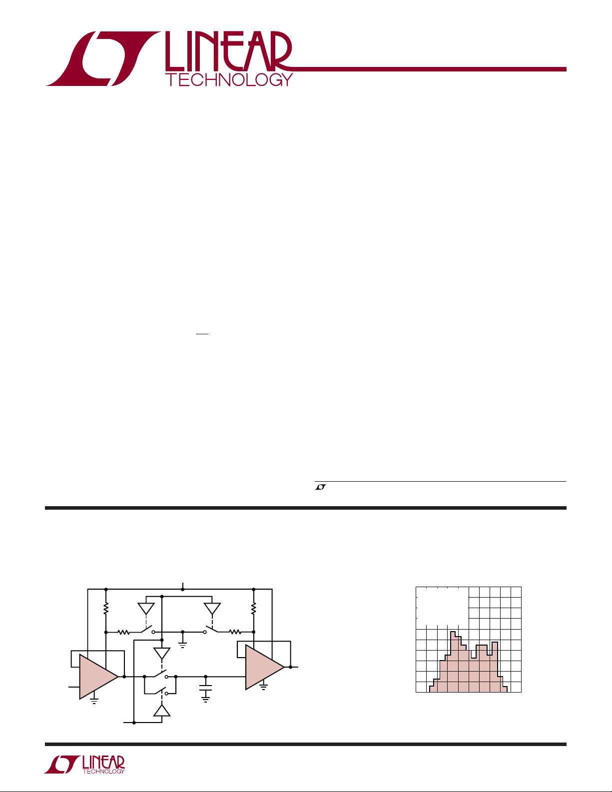
TYPICAL APPLICATIO
LT1006 Single Supply, Micropower Sample and Hold
9V
360k
1/4 CD4066
390Ω 390ΩS3 S4
2
3
INPUT
0V TO 5V
SAMPLE-HOLD COMMAND
7
–
A1
LT1006
+
4
HIGH = SAMPLE
LOW = HOLD
8
6
1/2 CD4066
S1
S2
1/2 CD4066
LT1006 • TA01
U
1/4 CD4066
0.01µF
360k
8
2
–
A2
LT1006
3
+
4
ACQUISITION TIME 20µs
HOLD SETTLING TIME 10µs
S-H OFFSET 1mV
HOLD SUPPLY CURRENT 250µA
SAMPLE SUPPLY CURRENT 5.0mA
1kHz SAMPLE RATE CURRENT 800µA
Distribution of Input Offset Voltage
20
VS = 5V, 0V
18
T
= 25°C
A
350 LT1006s TESTED
16
FROM TWO RUNS
14
J AND N PACKAGES
12
10
UNITS (%)
7
6
OUTPUT
8
6
4
2
0
–80
–40
INPUT OFFSET VOLTAGE (µV)
40 80
0
LT1006 • G01
1006fa
1
Page 2
LT1006
1
2
3
4
8
7
6
5
TOP VIEW
V
+
OUT
–IN
+IN
V
–
S8 PACKAGE
8-LEAD PLASTIC SO
N8 PACKAGE
8-LEAD PDIP
+
–
V
OS
TRIM
I
SY
SET
(NOTE 3)
V
OS
TRIM
(NOTE 4)
WWWU
ABSOLUTE AXI U RATI GS
(Note 1)
Supply Voltage ...................................................... ±22V
Input Voltage ............... Equal to Positive Supply Voltage
Input Voltage ............5V Below Negative Supply Voltage
Differential Input Voltage ......................................... 30V
Output Short-Circuit Duration .......................... Indefinite
UU
W
PACKAGE/ORDER I FOR ATIO
ORDER
TOP VIEW
ISY SET
(NOTE 3)
1
2
3
H PACKAGE
8
–
+
4
–
V
(CASE)
V
OS
TRIM
–IN
+IN
8-LEAD TO-5 METAL CAN
= 150°C, θJA = 150°C, θJC = 45°C
T
JMAX
V
7
6
5
V
TRIM
(NOTE 4)
+
OUT
OS
PART NUMBER
LT1006AMH
LT1006MH
LT1006ACH
LT1006CH
OBSOLETE PACKAGES
Consider the N8 or S8 Package for Alternate Source
Operating Temperature Range
LT1006AM/LT1006M (OBSOLETE)....– 55°C to 125°C
LT1006AC/LT1006C/LT1006S8 ............... 0°C to 70°C
Storage Temperature Range ................. – 65°C to 150°C
Lead Temperature (Soldering, 10 sec)..................300°C
ORDER
PART NUMBER
LT1006CN8
LT1006S8
S8 PART MARKING
T
= 100°C, θJA = 130°C/W (N8)
JMAX
T
= 150°C, θJA = 200°C/W (S8)
JMAX
J8 PACKAGE 8-LEAD CERDIP
T
= 100°C, θJA = 130°C/W
JMAX
1006
LT1006AMJ8
LT1006MJ8
LT1006ACJ8
LT1006CJ8
Consult LTC Marketing for parts specified with wider operating temperature ranges.
ELECTRICAL CHARACTERISTICS
VS = 5V, VCM = 0V, V
= 1.4V, TA = 25°C, unless otherwise noted.
OUT
LT1006AM/AC LT1006M/C
SYMBOL PARAMETER CONDITIONS MIN TYP MAX MIN TYP MAX UNITS
V
OS
Input Offset Voltage 20 50 30 80 µV
LT1006S8 80 400 µV
∆V
OS
Long-Term Input Offset 0.4 0.5 µV/Mo
∆Time Voltage Stability LT1006S8 0.7 µV/Mo
I
OS
I
B
e
n
Input Offset Current 0.12 0.5 0.15 0.9 nA
Input Bias Current 9 15 10 25 nA
Input Noise Voltage 0.1Hz to 10Hz 0.55 0.55 µV
Input Noise Voltage Density fO = 10Hz 23 32 23 32 nV/√Hz
f
= 1000Hz 22 25 22 25 nV/√Hz
O
i
n
Input Noise Current Density fO = 10Hz 0.07 0.08 pA/√Hz
Input Resistance (Note 2)
2
Differential Mode 180 400 100 300 MΩ
Common Mode 5 4 GΩ
P-P
1006fa
Page 3
LT1006
ELECTRICAL CHARACTERISTICS
SYMBOL PARAMETER CONDITIONS MIN TYP MAX MIN TYP MAX UNITS
Input Voltage Range 3.5 3.8 3.5 3.8 V
CMRR Common Mode Rejection Ratio VCM = 0V to 3.5V 100 114 97 112 dB
PSRR Power Supply Rejection Ratio VS = ±2V to ±18V, VO = 0V 106 126 103 124 dB
A
VOL
SR Slew Rate 0.25 0.4 0.25 0.4 V/µs
I
S
Large-Signal Voltage Gain VO = 0.03V to 4V, RL = 10k 1.0 2.5 0.7 2.0 V/µV
= 0.03V to 3.5V, RL = 2k 0.5 2.0 0.3 1.8 V/µV
V
O
Maximum Output Voltage Swing Output Low, No Load 15 25 15 25 mV
Output Low, 600Ω to GND 5 10 5 10 mV
Output Low, I
Output High, No Load 4.0 4.4 4.0 4.4 V
Output High, 600Ω to GND 3.4 4.0 3.4 4.0 V
Supply Current R
Minimum Supply Voltage 2.7 2.7 V
= ∞ 340 520 350 570 µA
SET
= 180k Pin 8 to Pin 7 (Note 3) 90 90 µA
R
SET
VS = 5V, VCM = 0V, V
= 1mA 220 350 220 350 mV
SINK
= 1.4V, TA = 25°C, unless otherwise noted.
OUT
LT1006AM/AC LT1006M/C
0–0.3 0 – 0.3 V
The ● denotes the specifications which apply over the full operating temperature range. VS = 5V, 0V; VCM = 0.1V; VO = 1.4V;
–55°C ≤ TA ≤ 125°C, unless otherwise noted.
LT1006AM LT1006M
SYMBOL PARAMETER CONDITIONS MIN TYP MAX MIN TYP MAX UNITS
V
OS
∆V
∆Temp
I
OS
I
B
A
VOL
CMRR Common Mode Rejection Ratio VCM = 0.1V to 3.2V ● 90 103 87 102 dB
PSRR Power Supply Rejection Ratio VS = ±2V to ±18V, VO = 0V ● 100 117 97 116 dB
I
S
Input Offset Voltage ● 40 180 60 250 µV
Input Offset Voltage Drift ● 0.2 1.3 0.3 1.8 µV/°C
OS
Input Offset Current ● 0.4 2.0 0.5 4.0 nA
Input Bias Current ● 13 25 16 40 nA
Large-Signal Voltage Gain VO = 0.05V to 3.5V, RL = 2k ● 0.25 0.8 0.15 0.7 V/µV
Maximum Output Voltage Swing Output Low, 600Ω to GND ● 615 618mV
Output High, 600Ω to GND
Supply Current ● 380 630 400 680 µA
● 3.2 3.8 3.1 3.8 V
1006fa
3
Page 4
LT1006
ELECTRICAL CHARACTERISTICS
temperature range. V
SYMBOL PARAMETER CONDITIONS MIN TYP MAX MIN TYP MAX UNITS
V
OS
∆V
∆Temp N8 Package
I
OS
I
B
A
VOL
CMRR Common Mode Rejection Ratio VCM = 0V to 3.4V ● 96 109 92 108 dB
PSRR Power Supply Rejection Ratio VS = ±2V to ±18V, VO = 0V ● 101 120 97 118 dB
I
S
Input Offset Voltage J8/H Package ● 30 110 45 160 µV
Input Offset Voltage Drift J8/H Package ● 0.2 1.3 0.3 1.8 µV/°C
OS
Input Offset Current ● 0.25 1.2 0.3 2.5 nA
Input Bias Current ● 11 20 12 30 nA
Large-Signal Voltage Gain VO = 0.04V to 3.5V, RL = 2k ● 0.35 1.3 0.25 1.2 V/µV
Maximum Output Voltage Swing Output Low, 600Ω to GND ● 613 613mV
Supply Current ● 350 570 360 620 µA
= 5V, 0V; VCM = 0V; VO = 1.4V; 0°C ≤ TA ≤ 70°C, unless otherwise noted.
S
N8 Package
S8 Package
S8 Package
Output High, 600Ω to GND
The ● denotes the specifications which apply over the full operating
LT1006AC LT1006C
● 50 190 µV
● 110 560 µV
● 0.5 2.5 µV/°C
● 0.7 3.5 µV/°C
● 3.3 3.9 3.2 3.9 V
VS = ±15V, TA = 25°C, unless otherwise noted.
LT1006AM/AC LT1006M/C
SYMBOL PARAMETER CONDITIONS MIN TYP MAX MIN TYP MAX UNITS
V
OS
I
OS
I
B
CMRR Common Mode Rejection Ratio VCM = +13.5V, –15V 100 117 97 116 dB
PSRR Power Supply Rejection Ratio VS = ±2V to ±18V, VO = 0V 106 126 103 124 dB
A
VOL
V
OUT
SR Slew Rate R
I
S
Input Offset Voltage 30 100 50 180 µV
LT1006S8 100 525 µV
Input Offset Current 0.1 0.5 0.15 0.9 nA
Input Bias Current 7.5 12.0 8 20 nA
Input Voltage Range 13.5 13.8 13.5 13.8 V
–15.0 –15.3 –15.0 –15.3 V
Large Signal Voltage Gain VO = ±10V, RL = 2k 1.5 5.0 1.2 4.0 V/µV
= ±10V, RL = 600Ω 0.8 1.5 0.5 1.0 V/µV
V
O
Maximum Output Voltage Swing RL = 2k ±13 ±14 ±12.5 ±14 V
= ∞ 0.25 0.4 0.25 0.4 V/µs
SET
R
= 390Ω Pin 8 to Pin 4 1.0 1.2 1.0 1.2 V/µs
SET
Supply Current 360 540 360 600 µA
4
1006fa
Page 5
LT1006
ELECTRICAL CHARACTERISTICS
temperature range. V
SYMBOL PARAMETER CONDITIONS MIN TYP MAX MIN TYP MAX UNITS
V
OS
∆V
∆Temp
I
OS
I
B
A
VOL
CMRR Common Mode Rejection Ratio VCM = +13V, –14.9V ● 97 114 94 113 dB
PSRR Power Supply Rejection Ratio VS = ±2V to ±18V, VO = 0V ● 100 117 97 116 dB
I
S
Input Offset Voltage ● 80 320 110 460 µV
Input Offset Voltage Drift ● 0.5 2.2 0.6 2.8 µV/°C
OS
Input Offset Current ● 0.2 2.0 0.3 3.0 nA
Input Bias Current ● 918 1127nA
Large-Signal Voltage Gain VO = ±10V, RL = 2k ● 0.5 1.5 0.25 1.0 V/µV
Maximum Output Voltage Swing RL = 2k ● ±12 ±13.8 ±11.5 ±13.8 V
Supply Current ● 400 650 400 750 µA
= ±15V, –55°C ≤ TA ≤ 125°C, unless otherwise noted.
S
The ● denotes the specifications which apply over the full operating
LT1006AM LT1006M
The ● denotes the specifications which apply over the full operating temperature range. VS = ±15V, 0°C ≤ TA ≤ 70°C, unless otherwise
noted.
LT1006AC LT1006C
SYMBOL PARAMETER CONDITIONS MIN TYP MAX MIN TYP MAX UNITS
V
OS
∆V
∆Temp N8 Package
I
OS
I
B
A
VOL
CMRR Common Mode Rejection Ratio VCM = 13V, –15V ● 98 116 94 114 dB
PSRR Power Supply Rejection Ratio VS = ±2V to ±18V, VO = 0V ● 101 120 97 118 dB
I
S
Input Offset Voltage J8/H Package ● 50 200 75 300 µV
N8 Package
S8 Package
Input Offset Voltage Drift J8/H Package ● 0.5 2.2 0.6 2.8 µV/°C
OS
S8 Package
Input Offset Current ● 0.15 1 0.25 2 nA
Input Bias Current ● 815 1023nA
Large-Signal Voltage Gain VO = ±10V, RL = 2k ● 13 0.7 2.5 V/µV
Maximum Output Voltage Swing RL = 2k ● ±12.5 ±13.9 ±11.5 ±13.8 V
Supply Current ● 370 600 380 660 µA
● 80 330 µV
● 150 730 µV
● 0.7 3.5 µV/°C
● 1.0 4.5 µV/°C
Note 1: Absolute Maximum Ratings are those values beyond which the life
of a device may be impaired.
Note 2: This parameter is guaranteed by design and is not tested.
Note 3: Regular operation does not require an external resistor. In order
to program the supply current for low power or high speed operation,
connect an external resistor from Pin 8 to Pin 7 or from Pin 8 to Pin 4,
respectively. Supply current specifications (for R
current in R
SET
.
= 180k) do not include
SET
Note 4: Optional offset nulling is accomplished with a potentiometer
connected between the trim terminals and the wiper to V
(providing a null range of ±6mV) is recommended for minimum drift of
nulled offset voltage with temperature. For increased trim resolution and
accuracy, two fixed resistors can be used in conjunction with a smaller
potentiometer. For example, two 4.7k resistors tied to Pins 1 and 5, with a
500Ω pot in the middle, will have a null range of ±150µV.
–
. A 10k pot
1006fa
5
Page 6

LT1006
UW
TYPICAL PERFOR A CE CHARACTERISTICS
Offset Voltage Drift with Temperature
of Representative Units
150
VS = 5V, 0V
120
–30
–60
OFFSET VOLTAGE (µV)
–90
–120
–150
= 0.1V
V
CM
90
60
30
0
50
–50
–25
25
0
TEMPERATURE (°C)
75
100
Warm-Up Drift
2.0
VS = 5V, 0V
T
= 25°C
A
1.5
1.0
0.5
CHANGE IN OFFSET VOLTAGE (µV)
0
LT1006 METAL CAN (H) PACKAGE
LT1006 CERDIP (J) PACKAGE
0
1
TIME AFTER POWER ON (MIN)
2
3
LT1006 • G02
LT1006 • G05
125
4
Offset Voltage vs Balanced Source
Resistor
INPUT OFFSET VOLTAGE (µV)
1.0
0.1
0.01
10
1k
VS = 5V, 0V, –55°C TO 125°C
R
S
–
R
S
+
VS = ±15V,
–55°C TO 125°C
VS = ±15V, 25°C
VS = 5V, 0V, 25°C
30k 100k3k 10k 300k 1M 3M 10M
BALANCED SOURCE RESISTANCE, RS (Ω)
Voltage Gain vs Load Resistance,
VS = 5V, 0V
10M
TA = –55°C
TA = 25°C
1M
TA = 125°C
VOLTAGE GAIN (V/V)
100k
100
LOAD RESISTANCE TO GROUND (Ω)
1k 10k
LT1006 • G03
LT1006 • G06
VOS vs Common Mode Voltage
vs Temperature
500
400
300
200
T =
125°C
1
T =
25°C
2
T =
125°C
1
2
OFFSET VOLTAGE (µV)
–100
–200
–300
100
0
–0.4
COMMON MODE INPUT VOLTAGE (V)
1
0 0.4 0.8 1.4
Voltage Gain vs Load Resistance
with VS = ±15V
10M
TA = 25°C
1M
VOLTAGE GAIN (V/V)
100k
100
LOAD RESISTANCE TO GROUND (Ω)
1k 10k
VS = 5V, 0V
T =
2
POSITIVE V
NEGATIVE V
1.0
LT1006 • G04
TA = –55°C
TA = 125°C
LT1006 • G07
25°C
OS
OS
Input Bias Current vs Temperature
18
VCM = 0V
15
12
9
6
INPUT BIAS CURRENT (nA)
3
0
–50
VS = 5V, 0V
–25 0
VS = ±15V
50 100 125
25 75
TEMPERATURE (˚C)
6
LT1006 • G08
Input Offset Current
vs Temperature
0.5
0.4
0.3
0.2
0.1
INPUT OFFSET CURRENT (nA)
0
–50
–25
VCM = 0V
VS = 5V, 0V
25
0
TEMPERATURE (°C)
VS = ±15V
50
75
100
LT1006 • G09
Input Bias Current
vs Common Mode Voltage
5
4
= 5V, 0V (V)
S
3
2
1
0
VS = ±15V,
–1
COMMON MODE INPUT VOLTAGE, V
125
0
VS = 5V, 0V, T = 125°C
T = 25°C
–6 –12
INPUT BIAS CURRENT (nA)
VS = 5V, 0V, T = 25°C
–18
LT1006 • G10
COMMON MODE INPUT VOLTAGE, V
15
10
5
0
–5
S
= 15V (V)
–10
–15
–24
1006fa
Page 7

UW
FREQUENCY (Hz)
10
0
COMMON MODE REJECTION RATIO (dB)
20
40
60
80
100
120
100 1k 10k 100k
LT1006 • G19
1M
TA = 25°C
VS = 5V, 0V VS = ±15V
TYPICAL PERFOR A CE CHARACTERISTICS
10Hz Voltage Noise Distribution 0.1Hz to 10Hz NoiseNoise Spectrum
VOLTAGE NOISE DENSITY (nV/√Hz)
1000
300
100
30
CURRENT NOISE DENSITY (fA/√Hz)
10
TA = 25°C
V
= ±2V TO ±18V
S
VOLTAGE NOISE
1/f CORNER 2Hz
1
CURRENT NOISE
10 100 1k
FREQUENCY (Hz)
100
80
60
40
NUMBER OF UNITS
20
0
16
20
VOLTAGE NOISE DENSITY (nV/√Hz)
VS = ±2.5V
T
= 25°C
A
200 UNITS TESTED
FROM THREE RUNS
24
28
32
LT1006 • G11
LT1006 • G12
VS = ±2V TO ±15V
= 25°C
T
A
NOISE VOLTAGE (100nV/DIV)
0
246
TIME (SEC)
LT1006
810
LT1006 • G13
Supply Current vs Temperature Increasing Slew Rate (R
500
450
400
350
SUPPLY CURRENT (µA)
300
250
–50
–25
VS = ±15V
VS = 5V, 0V
50
25
0
TEMPERATURE (°C)
75
Output Saturation vs Sink Current
vs Temperature
10
V+ = 5V TO 30V
–
= 0V
V
I
= 10mA
1.0
SINK
I
SINK
= 5mA
100
LT1006 • G14
125
1000
VS = 5V, 0V
SR
ISY*
100
SUPPLY CURRENT (µA)
PIN 8 IS APPROXIMATELY
60mV ABOVE THE NEGATIVE SUPPLY
10
50
CURRENT INJECTED INTO PIN 8 (µA)
DOES NOT INCLUDE CURRENT THROUGH R
*I
SY
5 0.510 1
Maximum Output Swing
vs Load Resistor
5
VS = 5V, 0V
4
3
TA = 125°C
TA = –55°C
LT1006 • G15
TA = 25°C
1
0.1
0.01
SET
10
SLEW RATE (V/µs)
1
SLEW RATE (V/µs)
PIN 8 IS APPROXIMATELY
60mV ABOVE THE NEGATIVE SUPPLY
0.1
100
SR
R
, PIN 8 TO PIN 4 (Ω)
SET
Common Mode Rejection Ratio
vs Frequency
to V–)Reducing Power Dissipation
SET
VS = ±15V
= 5V, 0V
OR V
S
I
SY
1k 10k
LT1006 • G16
10
SUPPLY CURRENT (mA)
1
0.1
0.1
SATURATION VOLTAGE (V)
0.01
–50 –25
0255075100 125
TEMPERATURE (°C)
I
SINK
I
SINK
I
SINK
I
SINK
= 1mA
= 100µA
= 10µA
= 0
LT1006 • G17
2
1
MAXIMUM OUTPUT VOLTAGE (V)
0
0.01
0.1 1 10
LOAD RESISTOR (kΩ)
LT1006 • G18
1006fa
7
Page 8
LT1006
UW
TYPICAL PERFOR A CE CHARACTERISTICS
Voltage Gain vs Frequency
140
120
100
80
60
40
VOLTAGE GAIN (dB)
20
0
–20
0.01
10.1 10 1k 100k 10M
VS = 5V, 0V VS = ±15V
100
FREQUENCY (Hz)
10k
TA = 25°C
C
= 10pF
L
1M
LT1006 • G20
20
10
GAIN
0
VOLTAGE GAIN (dB)
–10
5V, 0V 5V, 0V
0.1
0.3 3
TA = 25°C
V
= 0V
CM
C
= 10pF
PHASE
±15V
110
FREQUENCY (MHz)
L
±15V
LT1006 • G21
80
100
120
140
160
180
200
120
100
80
60
40
PHASE SHIFT (DEGREES)
20
POWER SUPPLY REJECTION RATIO (dB)
Power Supply Rejection Ratio
vs FrequencyGain, Phase vs Frequency
NEGATIVE
SUPPLY
VS = ±15V + 1Vp-p SINE WAVE
= 25°C
T
A
0
0.1
110
1k 100k 1M
100 10k
FREQUENCY (Hz)
POSITIVE
SUPPLY
LT1006 • G22
Large Transient Response,
VS = 5V, 0V
4V
2V
0V
AV = 1
= 4.7k TO 5V
R
L
INPUT = 0V TO 3.8V
10µs/DIV
Small-Signal Transient Response,
VS = 5V, 0V
100mV
1006 G23
Large-Signal Transient Response,
VS = 5V, 0V
4V
2V
0V
AV = 1
= 4.7k TO GROUND
R
L
INPUT = 0V TO 3.8V
10µs/DIV
20mV/DIV
Large-Signal Transient Response,
VS = ±15V
5V/DIV
1006 G24
AV = 1
50µs/DIV
Small-Signal Transient Response,
VCC = ±2.5V to ±15V
1006 G25
8
0V
AV = 1
C
= 10pF
L
= 600Ω TO GND
R
L
INPUT = 0V TO 100mV PULSE
20µs/DIV 1006 G26
AV = 1
C
= 10pF
L
2µs/DIV
1006 G27
1006fa
Page 9
WUUU
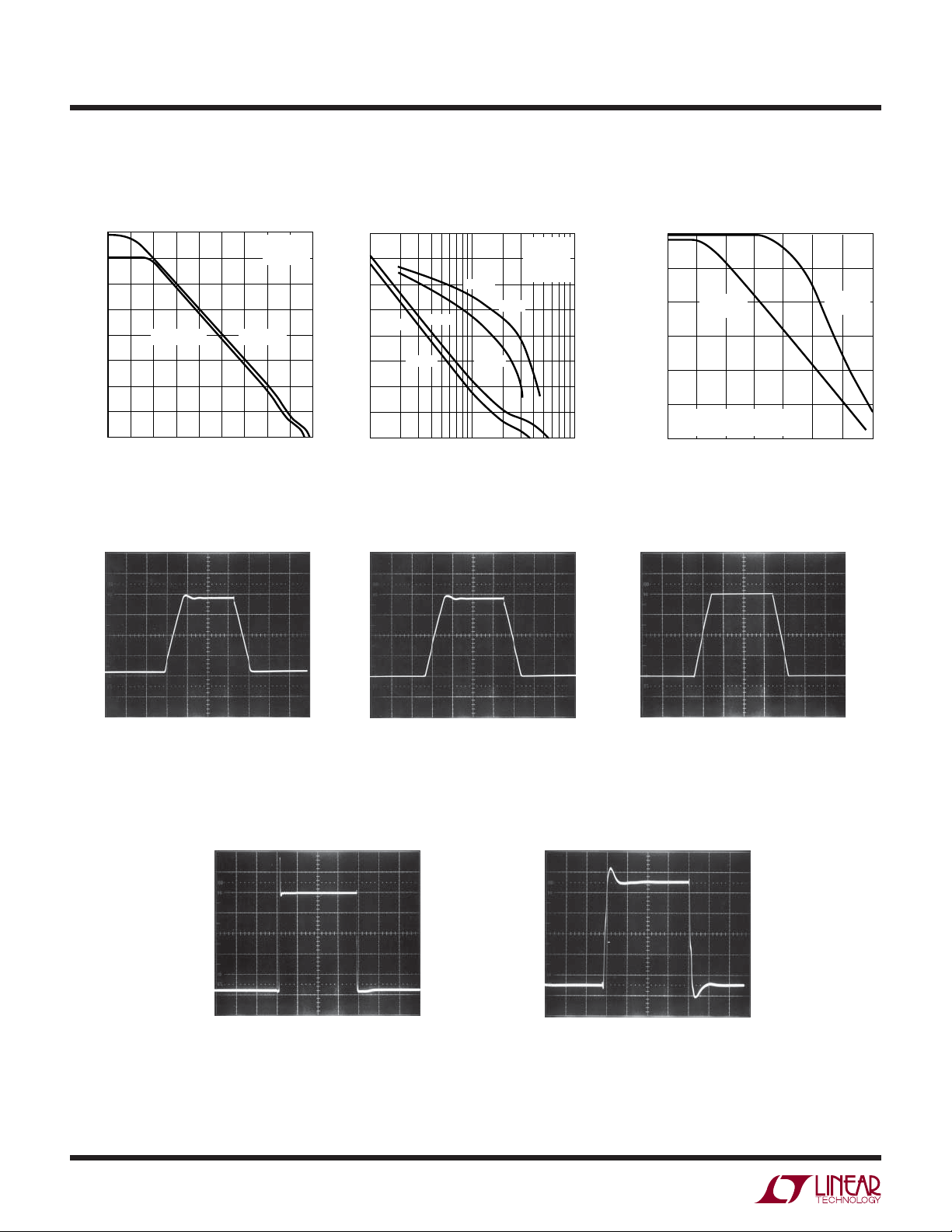
APPLICATIO S I FOR ATIO
LT1006
The LT1006 is fully specified for single supply operation,
(i.e., when the negative supply is 0V). Input common
mode range includes ground; the output swings within a
few millivolts of ground. Single supply operation, however, can create special difficulties, both at the input and
at the output. The LT1006 has specific circuitry which
addresses these problems.
At the input, the driving signal can fall below 0V—
inadvertently or on a transient basis. If the input is more
than a few hundred millivolts below ground, two distinct
problems can occur on previous single supply designs,
such as the LM124, LM158, OP-20, OP-21, OP-220,
OP-221, OP-420:
a) When the input is more than a diode drop below ground,
unlimited current will flow from the substrate (V– terminal) to the input. This can destroy the unit. On the LT1006,
the 400Ω resistors, in series with the input (see Schematic
Diagram), protect the devices even when the input is 5V
below ground.
b) When the input is more than 400mV below ground
(at 25°C), the input stage saturates (transistors Q3 and
Q4) and phase reversal occurs at the output. This can
cause lock-up in servo systems. Due to a unique phase
reversal protection circuitry (Q21, Q22, Q27, Q28), the
LT1006’s output does not reverse, as illustrated below,
even when the inputs are at –1.5V.
At the output, the aforementioned single supply designs
either cannot swing to within 600mV of ground (OP-20)
or cannot sink more than a few microamperes while
swinging to ground (LM124, LM158). The LT1006’s
all-NPN output stage maintains its low output resistance
and high gain characteristics until the output is saturated.
In dual supply operations, the output stage is crossover
distortion free.
Since the output cannot go exactly to ground, but can only
approach ground to within a few millivolts, care should be
exercised to ensure that the output is not saturated. For
example, a 1mV input signal will cause the amplifier to set
up in its linear region in the gain 100 configuration shown
below, but is not enough to make the amplifier function
properly in the voltage follower mode.
Voltage Follower with Input Exceeding the Negative Common Mode Range (VS = 5V, 0V)
4V
2V
0V
INPUT, –1.5V TO 4.5V 1006 TA11a
6V
P-P
R
1mV
–
+
5V
99R
LT1006
600Ω
100mV
LT1006 • TA02
4V
2V
0V
LM324, LM358, OP-20, OP-21
EXHIBIT OUTPUT PHASE
REVERSAL
1006 TA11b
1mV
4V
2V
0V
LT1006
NO PHASE REVERSAL
Voltage FollowerGain 100 Amplifier
5V
–
+
LT1006
600Ω
OUTPUT
SATURATED
≈ 5mV
LT1006 • TA03
1006 TA11c
1006fa
9
Page 10
LT1006
WUUU
APPLICATIO S I FOR ATIO
In automated production testing the output is forced to
1.4V by the test loop; offset voltage is measured with a
common mode voltage of zero and the negative supply at
zero (Pin 4). Without the test loop, these exact conditions
cannot be achieved. The test circuit shown ensures that
the output will never saturate even with worst-case offset
voltages (–250µV over the –55°C to 125°C range). The
effective common mode input is 0.3V with respect to the
negative supply. As indicated by the common mode rejection specifications the difference is only a few microvolts
between the two methods of offset voltage measurement.
Test Circuit for Offset Voltage and
Offset Drift with Temperature
50k*
4.7V
–
LT1006 • TA04
V
0
100Ω
50k*
LT1006
+
–0.3V
***RESISTORS MUST HAVE LOW
THERMOELECTRIC POTENTIAL.
THIS CIRCUIT IS ALSO USED AS
THE BURN-IN CONFIGURATION,
WITH SUPPLY VOLTAGES
INCREASED TO ± 20V
= 1000V
V
O
OS
Low Supply Operation
The minimum guaranteed supply voltage for proper
operation of the LT1006 is 2.7V. Typical supply current at
this voltage is 320µA; therefore, power dissipation is only
860µW.
Noise Testing
For application information on noise testing and
calculations, please see the LT1007 or LT1028 data sheet.
Supply Current Programming
Connecting an optional external resistor to Pin 8 changes
the biasing of the LT1006 in order to increase its speed or
to decrease its power consumption. If a higher slew rate is
required, connect the external resistor for Pin 8 to Pin 4
[see performance curves for Increasing Slew Rate
(R
to V–)]. For lower power consumption, inject a
SET
current into Pin 8 (which is approximately 60mV above
V–) as shown on the Reducing Power Dissipation plot.
This can be accomplished by connecting R
SET
to the
positive supply, or to save additional power, by obtaining
the injected current from a low voltage battery.
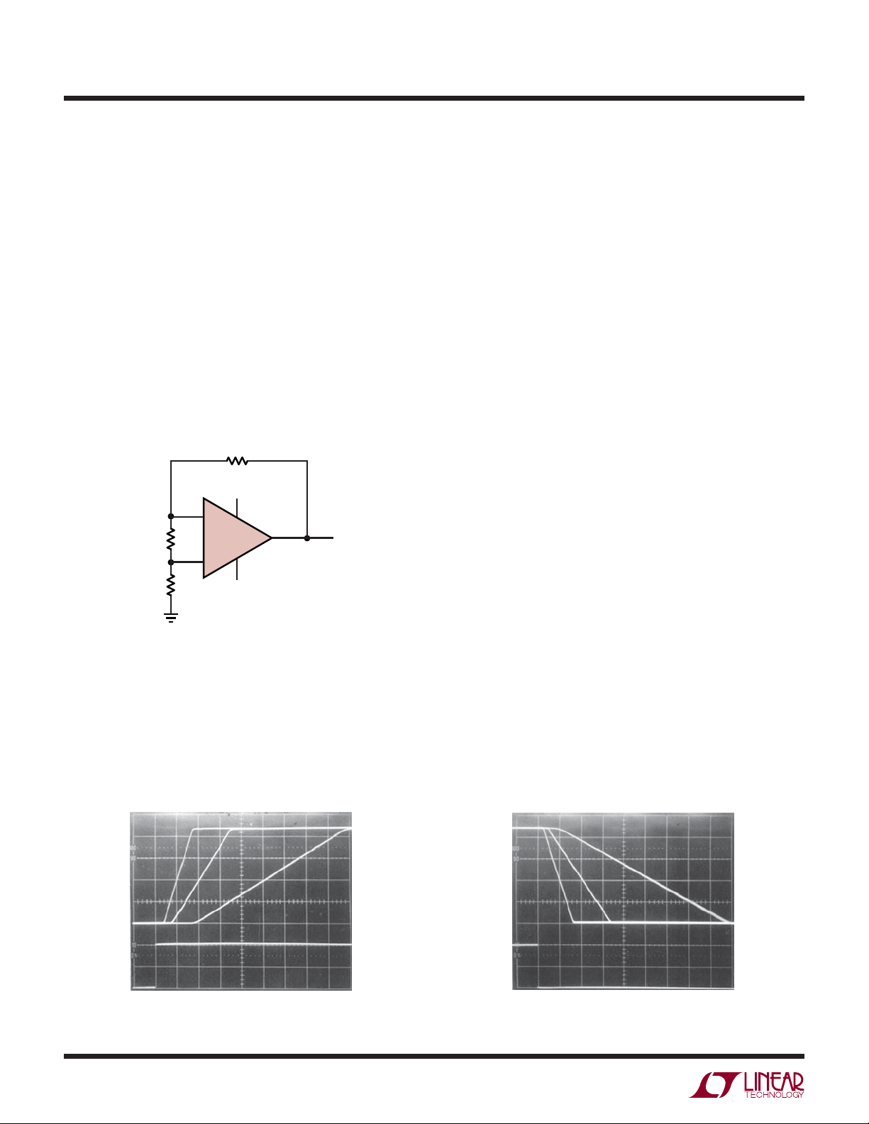
Comparator Applications
The single supply operation of the LT1006 and its ability to
swing close to ground while sinking current lends itself
to use as a precision comparator with TTL compatible
output.
OUTPUT (V)
INPUT (mV)
10
Comparator Rise Response Time
to 10mV, 5mV, 2mV Overdrives
4
2
0
0
–100
= 5V, 0V 50µs/DIV 1006 TA12a
V
S
OUTPUT (V)
INPUT (mV)
Comparator Fall Response Time
to 10mV, 5mV, 2mV Overdrives
4
2
0
0
–100
0
= 5V, 0V 50µs/DIV 1006 TA12b
V
S
1006fa
Page 11

TYPICAL APPLICATIO S
U
LT1006
I
50k
5°C
TRIM
Platinum RTD Signal Conditioner
with Curvature Correction
+V
V = 5.6V TO 10V
39k
LM334
1.21k*
= 100µA
K
10k*
1k**
1N457
1k**
1k @
0°C
R
P
43.2k**
12k*
1k**
–
+
1µF
= ROSEMOUNT 118MF
R
P
** = TRW MAR-6 0.1%
* = 1% METAL FILM
1µF
7
LT1006
1.21M*
400°C
TRIM
+V
4
5k
180k
8
0.02V TO 4V OUT =
2°C TO 400°C
±0.25°C
LT1006 • TA05
Voltage Controlled Current Source
with Ground Referred Input and Output
5V
3
INPUT
0V TO 2V
1k
1µF
7
+
LT1006
2
–
8 7
14 13
1/2 LTC1043
17 16
OPERATES FROM A SINGLE 5V SUPPLY
4
0.68µF
5V
4
11
12
0.001µF
1µF
6
100Ω
=
I
OUT
LT1006 • TA06
V
IN
100Ω
3.1k*
200k*
INPUT
0V TO 5V
*= 1% METAL FILM
** = 1% METAL FILM, SELECTED
= 2N3904
= 74C14
120k**
TYP
20k
1MHz
TRIM
2µF
100Hz
TRIM
220k** TYP
2k
Q5
Q6
+
A1
LT1006
–
0.33µF
Micropower 1MHz V/F Converter
9V
LM334
2k*
VOLTAGE
9V
470k
7
8
47k
4
0.01µF
CONTROLLED
CURRENT
SOURCE
12k
Q8
2N3906
1000pF
(POLYSTYRENE)
CHARGE PUMP
3pF 1N4148
TRIGGER
STRAY
CAPACITANCE
Q1
NC
Q7
+
10µF
112
74C90
1414
REFERENCE
SWITCH
11
14
÷100
112
74C90
Q2
Q3
REFERENCE
11
Q4
LT1004-2.5
LT1004-1.2
OUTPUT
0MHz TO 1MHz
0.12% LINEARITY
280µA QUIESCENT CURRENT
680µA AT 1MHz
LT1006 • TA07
1006fa
11
Page 12

LT1006
TYPICAL APPLICATIO S
Micropower Thermocouple Signal Conditioner with Cold Junction Compensation
100k
U
4.5V
(3AA CELLS)
R4
233k*
LT1004
1.235V
CATALYST
RESEARCH CORP
MODEL 2736
5V
10k
5%
3.2k
6250Ω
2.8V
TYPE J THERMOCOUPLE
1k
16.2k
0°C
T1
LT1034
1.2V
107k
R1
1684*
R2
186*
R3
R
T
1.8k*
Linear Thermometer
4
1/2 LTC1043
7 8
11
1µF
12
13
+
LT1006
–
14
56k
7
8
4
5.98k*
1µF
0V TO 3V OUT =
0°C TO 60°C
±0.75°C
5.76M*
TOTAL POWER CONSUMPTION ≤ 500µW
* = TRW MAR-6 0.1%
= YELLOW SPRINGS INST. CO
R
T
MODEL 44007 5k AT 25°C
5V
3
7
2
+
LT1006
–
6
4
51.1k
500Ω
100°C
100k
LT1006 • TA08
0V TO 1.000V =
0°C TO 100.0°C ±0.25°C
12
0.001µF
1716
T1 = YELLOW SPRINGS #44201
ALL RESISTORS = TRW MAR-6 0.1% UNLESS NOTED
LT1006 • TA09
1006fa
Page 13
TYPICAL APPLICATIO S
U
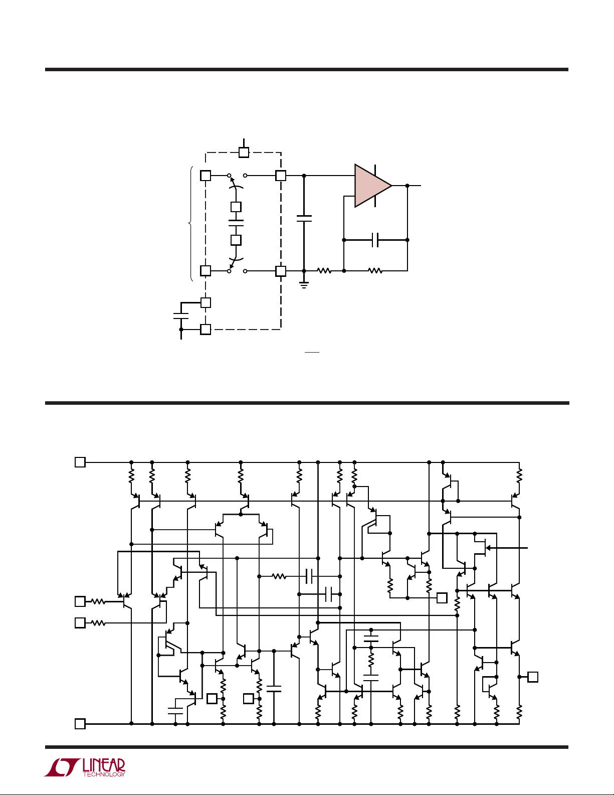
±5V Precision Instrumentation Amplifier
5V
LT1006
DIFFERENTIAL
INPUT
0.01µF
–5V
W
W
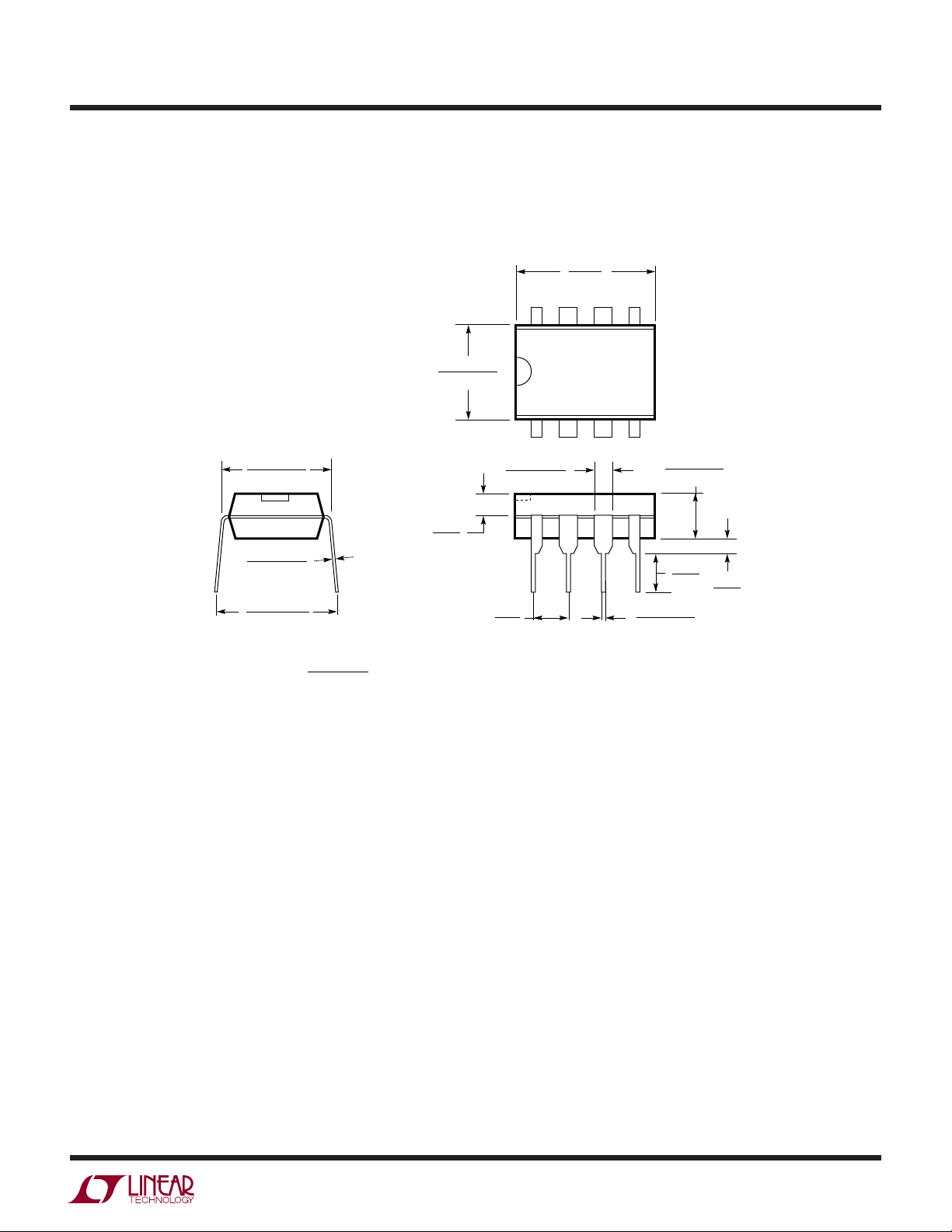
SCHE ATIC DIAGRA
4
+
7 8
11
C1
1µF
(EXTERNAL)
12
13
16
1/2 LTC1043
17
5V
3
8
+
LT1006
2
–
C2
1µF
14
CMRR > 120dB AT DC
CMRR > 120dB AT 60Hz
DUAL SUPPLY OR SINGLE 5V
GAIN = 1 + R2/R1
≈ 150µV
V
OS
∆V
OS
≈ 2µV/°C
∆T
COMMON MODE INPUT VOLTAGE INCLUDES THE SUPPLIES
1
4
–5V
1µF
R2R1
V
OUT
LT1006 • TA10
V
+IN
–IN
V
+
7
9k 9k 1.6k
Q6
Q22
3
400Ω
2
400Ω
–
4
Q2
Q5 Q13
Q27
Q21
Q1
Q12
75pF
Q28
Q11
Q9
1
TRIM
1.6k 1.6k
Q16 Q14
Q3
Q7
Q4
Q29
Q8
2.7k2k2.7k
5
TRIM
100Ω
Q15 Q32
21pF
3.9k
2.5pF
Q18
Q10
15pF
Q17
2k 2k 1.3k
1k 600Ω
Q30
Q19
Q20
Q25
2.4k 18Ω
4pF
2k
100pF
Q23
Q33
Q26
OUTPUT
Q31
Q34
Q24
2k 30Ω
Q38
Q35
6
Q37
J1
Q39 Q40
28k
Q42
84k 2.5k5.4k
Q44
LT1006 • SD01
Q36
Q41
Q43
–
V
8
1006fa
13
Page 14

LT1006
PACKAGE DESCRIPTIO
U
H Package
8-Lead TO-5 Metal Can (.200 Inch PCD)
(Reference LTC DWG # 05-08-1320)
.335 – .370
(8.509 – 9.398)
DIA
.305 – .335
(7.747 – 8.509)
.016 – .021**
(0.406 – 0.533)
.027 – .045
(0.686 – 1.143)
PIN 1
SEATING
PLANE
45°TYP
.010 – .045*
(0.254 – 1.143)
.028 – .034
(0.711 – 0.864)
.040
(1.016)
MAX
.050
(1.270)
MAX
GAUGE
PLANE
.200
(5.080)
TYP
.165 – .185
(4.191 – 4.699)
.500 – .750
(12.700 – 19.050)
REFERENCE
PLANE
.110 – .160
(2.794 – 4.064)
INSULATING
STANDOFF
*
LEAD DIAMETER IS UNCONTROLLED BETWEEN THE REFERENCE PLANE
AND THE SEATING PLANE
**
FOR SOLDER DIP LEAD FINISH, LEAD DIAMETER IS
8-Lead CERDIP (Narrow .300 Inch, Hermetic)
(Reference LTC DWG # 05-08-1110)
CORNER LEADS OPTION
(4 PLCS)
.023 – .045
(0.584 – 1.143)
HALF LEAD
.045 – .068
(1.143 – 1.650)
FULL LEAD
OPTION
.300 BSC
(7.62 BSC)
.008 – .018
(0.203 – 0.457)
NOTE: LEAD DIMENSIONS APPLY TO SOLDER DIP/PLATE
OR TIN PLATE LEADS
OPTION
0° – 15°
J8 Package
.005
(0.127)
MIN
.025
(0.635)
RAD TYP
.045 – .065
(1.143 – 1.651)
.014 – .026
(0.360 – 0.660)
.016 – .024
(0.406 – 0.610)
.405
(10.287)
MAX
87
12
H8(TO-5) 0.200 PCD 0801
65
3
4
.220 – .310
(5.588 – 7.874)
.015 – .060
(0.381 – 1.524)
.100
(2.54)
BSC
.200
(5.080)
MAX
.125
3.175
MIN
J8 0801
14
OBSOLETE PACKAGES
1006fa
Page 15
PACKAGE DESCRIPTIO
U
N8 Package
8-Lead PDIP (Narrow .300 Inch)
(Reference LTC DWG # 05-08-1510)
.255 ± .015*
(6.477 ± 0.381)
.400*
(10.160)
MAX
87 6
LT1006
5
12
.300 – .325
(7.620 – 8.255)
.065
(1.651)
.008 – .015
(0.203 – 0.381)
+.035
.325
–.015
+0.889
8.255
()
–0.381
NOTE:
1. DIMENSIONS ARE
*THESE DIMENSIONS DO NOT INCLUDE MOLD FLASH OR PROTRUSIONS.
MOLD FLASH OR PROTRUSIONS SHALL NOT EXCEED .010 INCH (0.254mm)
INCHES
MILLIMETERS
TYP
.045 – .065
(1.143 – 1.651)
.100
(2.54)
BSC
3
4
.130 ± .005
(3.302 ± 0.127)
.120
(3.048)
MIN
.018 ± .003
(0.457 ± 0.076)
.020
(0.508)
MIN
N8 1002
Information furnished by Linear Technology Corporation is believed to be accurate and reliable.
However, no responsibility is assumed for its use. Linear Technology Corporation makes no representation that the interconnection of its circuits as described herein will not infringe on existing patent rights.
1006fa
15
Page 16

LT1006
PACKAGE DESCRIPTIO
.050 BSC
N
U
S8 Package
8-Lead Plastic Small Outline (Narrow .150 Inch)
(Reference LTC DWG # 05-08-1610)
.189 – .197
.045 ±.005
(4.801 – 5.004)
8
NOTE 3
7
5
6
.245
MIN
123 N/2
.030 ±.005
TYP
RECOMMENDED SOLDER PAD LAYOUT
.010 – .020
(0.254 – 0.508)
.008 – .010
(0.203 – 0.254)
NOTE:
1. DIMENSIONS IN
2. DRAWING NOT TO SCALE
3. THESE DIMENSIONS DO NOT INCLUDE MOLD FLASH OR PROTRUSIONS.
MOLD FLASH OR PROTRUSIONS SHALL NOT EXCEED .006" (0.15mm)
×
°
45
.016 – .050
(0.406 – 1.270)
INCHES
(MILLIMETERS)
.160
0°– 8° TYP
±.005
.228 – .244
(5.791 – 6.197)
.053 – .069
(1.346 – 1.752)
.014 – .019
(0.355 – 0.483)
TYP
N
.150 – .157
(3.810 – 3.988)
N/2
1
3
2
NOTE 3
4
.004 – .010
(0.101 – 0.254)
.050
(1.270)
BSC
SO8 0502
16
Linear Technology Corporation
1630 McCarthy Blvd., Milpitas, CA 95035-7417
(408) 432-1900 ● FAX: (408) 434-0507
●
www.linear.com
1006fa
LT/TP 1102 1K REV A • PRINTED IN USA
LINE AR TE CHNO LOGY CORPO R ATION 1988
 Loading...