

Page 1
High Speed Converter Evaluation Platform
FEATURES
Xilinx Virtex-4 FPGA-based buffer memory board
Used for capturing digital data from high speed ADC
evaluation boards to simplify evaluation
64 kB FIFO depth
Parallel input at 644 MSPS SDR and 800 MSPS DDR
Supports 1.8 V, 2.5 V, and 3.3 V CMOS and LVDS interfaces
Supports multiple ADC channels up to 18 bits
Measures performance with VisualAnalog
Real-time FFT and time domain analysis
Analyzes SNR, SINAD, SFDR, and harmonics
Simple USB port interface (2.0)
Supports ADCs with serial port interfaces (SPI)
FPGA reconfigurable via JTAG, on-board EPROM, or USB
On-board regulator circuit speeds setup
5 V, 3 A switching power supply included
Compatible with Windows 98 (2nd edition), Windows 2000,
Windows ME, and Windows XP
EQUIPMENT NEEDED
Analog signal source and antialiasing filter
Low jitter clock source
High speed ADC evaluation board and ADC data sheet
PC running Windows 98 (2nd edition), Windows 2000,
Windows ME, or Windows XP
Latest version of VisualAnalog
USB 2.0 port recommended (USB 1.1 compatible)
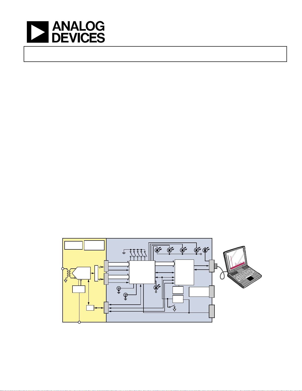
FUNCTIONAL BLOCK DIAGRAM
HSC-ADC-EVALC
PRODUCT HIGHLIGHTS
1. Easy to Set Up. Connect the included power supply along
with the CLK and AIN signal sources to the two evaluation
boards. Then connect to the PC via the USB port and
evaluate the performance instantly.
2. USB Port Connection to PC. PC interface is via a USB 2.0
connection (1.1 compatible) to the PC. A USB cable is
provided in the kit.
3. 64 kB FIFO. The on-board FPGA contains an integrated
FIFO to store data captured from the ADC for subsequent
processing.
4. Up to 644 MSPS SDR/800 MSPS DDR Encode Rates on
Each Channel. Multichannel ADCs with encode rates up
to 644 MSPS SDR and 800 MSPS DDR can be used with
the ADC capture board.
5. Supports ADCs with Serial Port Interface or SPI. Some
ADCs include a feature set that can be changed via the
SPI. The ADC capture board supports these SPI-driven
features through the existing USB connection to the
computer without additional cabling needed.
6. VisualAnalog™. VisualAnalog supports the HSC-ADC-
EVALC hardware platform as well as enabling virtual ADC
evaluation using ADIsimADC™, Analog Devices proprietary
behavioral modeling technology. This allows rapid comparison between multiple ADCs, with or without hardware
evaluation boards. For more information, see AN-737 at
www.analog.com/VisualAnalog.
CLOCK
CIRCUIT
REGULATORS
ADC
ON-BOARD
VOLTAGE
LOGIC
SPI
POWER
CONNECTOR
SINGLE OR MULTICHANNEL
HIGH SPEED ADC
EVALUATION BOARD
FILTERED
ANALOG
INPUT
CLOCK INP UT
Rev. 0
Evaluation boards are only intended for device evaluation and not for production purposes.
Evaluation boards as supplied “as is” and without warranties of any kind, express, implied, or
statutory including, but not limited to, any implied warranty of merchantability or fitness for a
particular purpose. No license is granted by implication or otherwise under any patents or other
intellectual property by application or use of evaluation boards. Information furnished by Analog
Devices is believed to be accurate and reliable. However, no responsibility is assumed by Analog
Devices for its use, nor for any infringements of pate nts or other rights of third parties t hat may result
from its use. Analog Devices reserves the right to change devices or specifications at any time
without notice. Trademarks and registered trademarks are the property of their respective owners.
Evaluation boards are not authorized to be used in life support devices or systems.
HSC-ADC-EVALC
FPGA
CONFIGURATION
MODE
DATA BUS 2(18 )
n
J3*
CLKA(2)
DATA BUS 1(18 )
n
J2*
CLKB(2)
EXT SYNC1
EXT SYNC2
FPGA GPIO(8)
SPI(7)
J1*
USB DIRECT( 5 )
*DATA CONVE RTE R I/O CONNECTORS
FPGA
LED2 LED1
FPGA
DONE
Figure 1.
USB
CAPTUREUPLOAD
DATA(16)
FIFO
CONTROL(9)
PORTB
PORTD
USB
CONTROLLER
PORTC
PORTE
PORTA
USB
CONFIG
PROM
FPGA
CONFIG
PROM
RECONFIG
CONNECTOR
ONBOARD
VOLTAGE
REGULATORS
POWER
CONNECTOR
JTAG
CONNECTOR
USB
J6
J4
J10
STANDARD
USB 2.0
06676-001
One Technology Way, P.O. Box 9106, Norwood, MA 02062-9106, U.S.A.
Tel: 781.329.4700 www.analog.com
Fax: 781.461.3113 ©2007 Analog Devices, Inc. All rights reserved.
Page 2

HSC-ADC-EVALC
TABLE OF CONTENTS
Features.............................................................................................. 1
Equipment Needed........................................................................... 1
Product Highlights ........................................................................... 1
Functional Block Diagram .............................................................. 1
Revision History ............................................................................... 2
Product Description......................................................................... 3
Evaluation Board Description......................................................... 3
Evaluation Board Hardware............................................................ 4
HSC-ADC-EVALC ADC Capture Board Easy Start ............... 4
Power Supplies .............................................................................. 4
Connection and Setup ................................................................. 4
Jumpers.......................................................................................... 5
HSC-ADC-EVALC ADC Capture Board Features.................. 6
HSC-ADC-EVALC Supported ADC Evaluation Boards........ 7
Theory of Operation .........................................................................8
Configuration ................................................................................8
Input Circuitry...............................................................................8
Data Capture..................................................................................8
Code Description ..........................................................................8
FPGA Configuration and Customization..................................8
Evaluation Board Schematics and Artwork...................................9
HSC-ADC-EVALC Schematics...................................................9
PCB Layout ................................................................................. 23
I/O Connector—J1, J2, and J3 Pin Mapping .......................... 24
Ordering Information.................................................................... 28
Bill of Materials (RoHS Compliant) ........................................ 28
Ordering Guide .......................................................................... 30
ESD Caution................................................................................ 30
REVISION HISTORY
4/07—Revision 0: Initial Version
Rev. 0 | Page 2 of 32
Page 3

HSC-ADC-EVALC
PRODUCT DESCRIPTION
The Analog Devices, Inc. high speed converter evaluation
platform (HSC-ADC-EVALC) includes the latest version of
VisualAnalog and an FPGA-based buffer memory board to capture
blocks of digital data from the Analog Devices high speed
analog-to-digital converter (ADC) evaluation boards. The ADC
capture board is connected to the PC through a USB port and is
used with VisualAnalog to quickly evaluate the performance of
high speed ADCs. Users can view an FFT for a specific analog
input and encode rate to analyze SNR, SINAD, SFDR, and
harmonic information.
The ADC capture board is easy to set up. Additional equipment
needed includes an Analog Devices high speed ADC evaluation
board, a signal source, and a clock source. Once the kit is
connected and powered, the evaluation is enabled instantly on
the PC.
The ADC capture board enables numerous expansion and
evaluation possibilities by virtue of its powerful reconfigurable
FPGA core.
The system can acquire digital data at speeds up to 644 MSPS
single data rate (SDR) and 800 MSPS double data rate (DDR).
The FPGA contains an integrated FIFO memory that allows
capture of data record lengths up to a total of 64 kB. A USB 2.0
microcontroller communicating with VisualAnalog allows
for easy interfacing to newer computers using the USB 2.0
(USB 1.1 compatible) interface.
EVALUATION BOARD DESCRIPTION
The ADC capture board provides all of the support circuitry
required to accept two 18-bit channels from an ADC’s parallel
CMOS or LVDS outputs. Various functions such as FPGA
configuration load options and I/O logic levels can be selected by
proper connection of various jumpers or switches (see
When using the HSC-ADC-EVALC in conjunction with an
ADC evaluation board, it is critical that the signal sources used
for the ADC board’s analog input and clock have very low phase
noise (<1 ps rms jitter) to achieve the ultimate performance of
the converter.
Proper filtering of the analog input signal to remove harmonics
and lower the integrated or broadband noise at the input is also
necessary to achieve the specified noise performance.
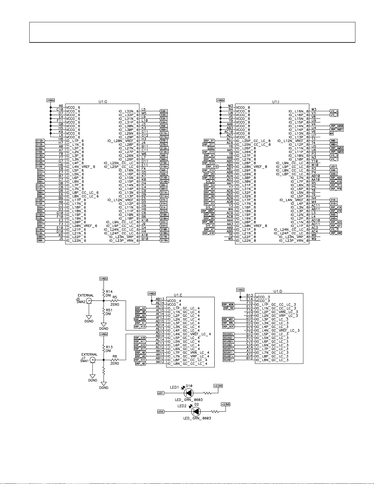
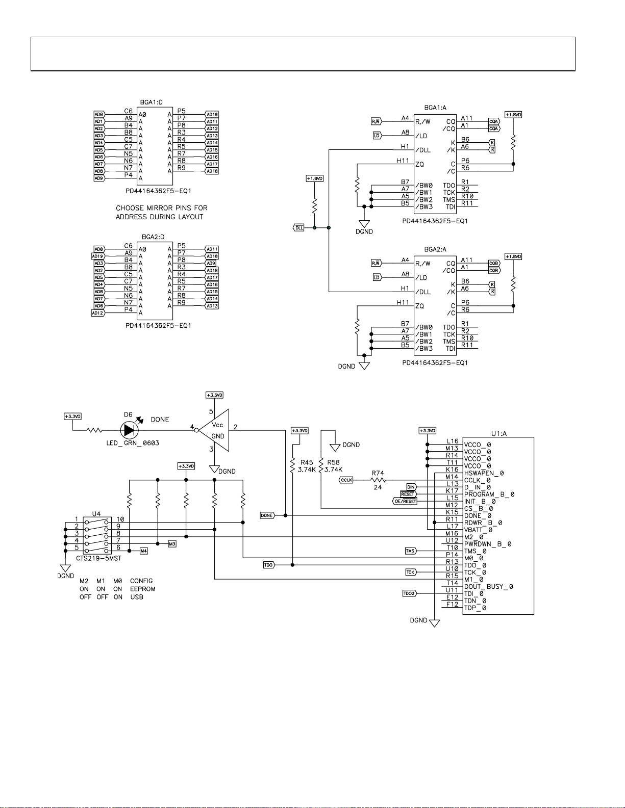
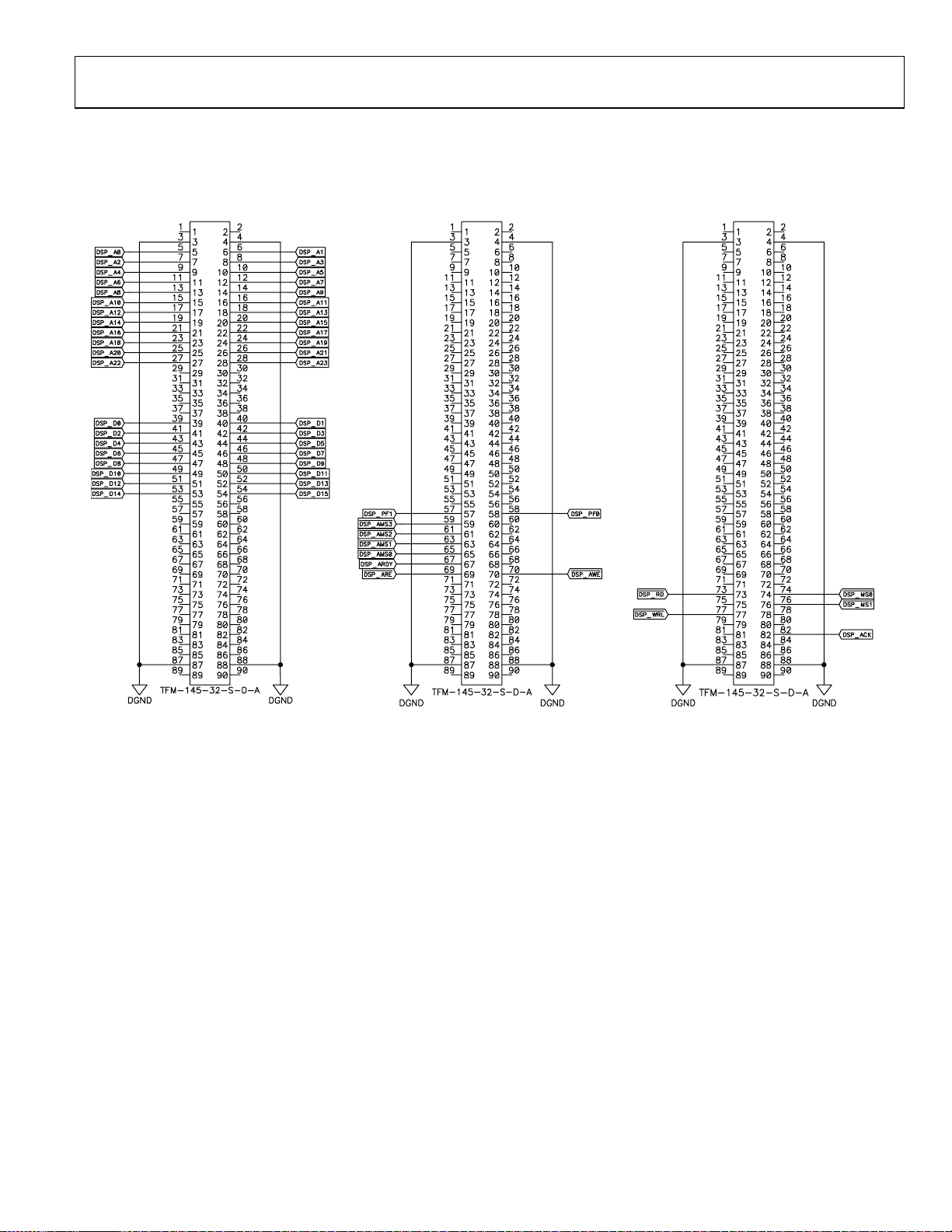
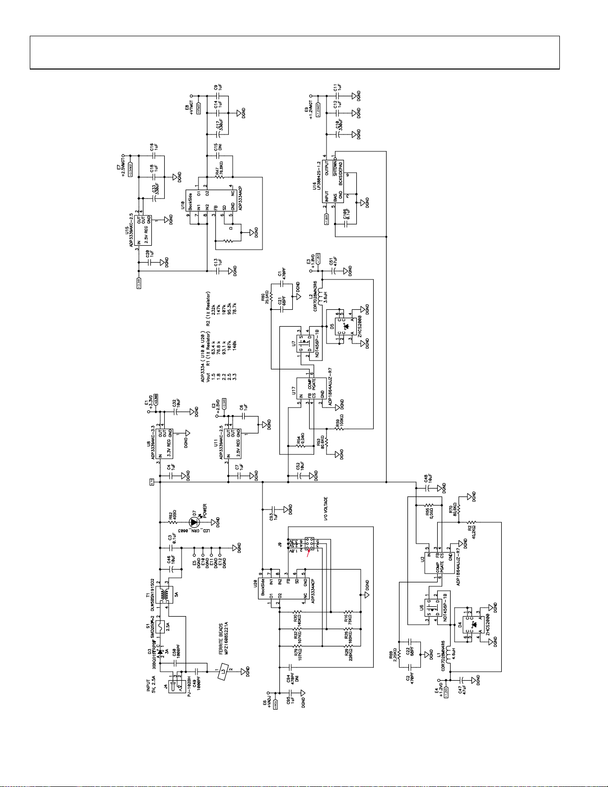
Figure 5 to Figure 20 for complete schematics and layout plots.
See
Tabl e 1).
Rev. 0 | Page 3 of 32
Page 4

HSC-ADC-EVALC
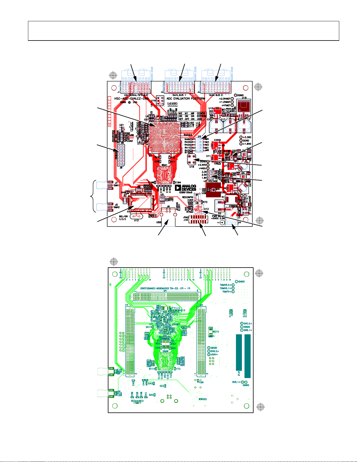
EVALUATION BOARD HARDWARE
HSC-ADC-EVALC ADC CAPTURE BOARD
EASY START
Requirements
• HSC-ADC-EVALC ADC capture board, VisualAnalog, 5 V
wall transformer, and USB cable
• High speed ADC evaluation board and ADC data sheet
• Power supply for ADC evaluation board
• Analog signal source and appropriate filtering
• Low jitter clock source applicable for specific ADC
evaluation, typically <1 ps rms jitter
• PC running Windows® 98 (2nd edition), Windows 2000,
Windows ME, or Windows XP
• PC with a USB 2.0 port recommended (USB 1.1 compatible)
Easy Start Steps
Important Note
Administrative rights for the Windows operating systems are
needed during the entire easy start procedure.
Completion of every step before reverting to a normal user
mode is recommended.
1. Install VisualAnalog from the CD provided in the ADC
capture board kit or download the latest version from the
Web. For the latest updates to the software, check the
Analog Devices website at
2. Connect the ADC capture board to the ADC evaluation
board. If an adapter is required, insert the adapter between
the ADC evaluation board and the ADC capture board.
3. Connect the provided USB cable to the ADC capture board
and to an available USB port on the computer.
4. Refer to
logic level to match the level coming from the ADC evaluation board. 1.8 V is default; 2.5 V and 3.3 V are jumper
selectable. Most evaluation boards can be used with the
default settings.
5. The ADC capture board is supplied with a wall mount
switching power supply. Connect the supply end to an ac
wall outlet rated for 100 Vac to 240 Vac at 47 Hz to 63 Hz.
The other end is a 2.1 mm inner diameter jack that connects
to the PCB at J4.
Table 1 for setting the ADC capture board’s I/O
www.analog.com/FIFO.
6. Once the USB cable is connected to both the computer and
the HSC-ADC-EVALC board, and power is applied, the
USB driver starts to install. The Found New Hardware
Wizard opens and prompts you through the automated
install process.
7. (Optional) Verify in the Windows device manager that
Analog Devices ADC-HSC-EVALC is listed under the
USB hardware.
8. Refer to the instructions included in the respective ADC
data sheet found at
information about connecting the ADC evaluation board’s
power supply and other requirements. After verification of
power supply connections, apply power to the ADC
evaluation board and check the voltage levels on the ADC
board to make sure they are correct.
9. Make sure the evaluation boards are powered on before
connecting the analog input and clock. Connect the
appropriate analog input (which should be filtered with a
band-pass filter) and low jitter clock signal.
10. Refer to the VisualAnalog User Manual at
www.analog.com/FIFO for detailed software operating
instructions.
www.analog.com/FIFO for more
POWER SUPPLIES
The ADC capture board is supplied with a wall mount switching power supply that provides a 5 V, 3 A maximum output.
Connect the supply to the rated 100 Vac to 240 Vac wall outlet at
47 Hz to 63 Hz. The other end is a 2.1 mm inner diameter jack
that connects to the PCB at J4. On the PC board, the supply is
fused and conditioned before connecting to the regulators that
supply the proper bias to the entire ADC capture board.
CONNECTION AND SETUP
The ADC capture board has two 40-pin connectors (J2 and J3)
that accept two 18-bit channels of parallel CMOS or LVDS
inputs from the ADC (see
(J1) is used to pass SPI and other USB/FPGA control signals
across to adjacent ADC evaluation boards that support these
features.
Figure 2). The third 40-pin connector
Rev. 0 | Page 4 of 32
Page 5
HSC-ADC-EVALC
T
WALL OUTLE
100V TO 240V AC
47Hz TO 63Hz
ROHDE & SCHWARZ,
SMHU,
2V p-p SIGNAL
SYNTHESIZER
ROHDE & SCHWARZ,
SMHU,
2V p-p SIGNAL
SYNTHESIZER
SWITCHING
POWER
SUPPLY
BAND-PASS
FILTER
EVALUATION
BOARD
XFMR
INPUT
CLK
DATA BUS 2
PARALLEL
LVDS/ CMOS
OUTPUTS
DATA BUS 1
PARALLEL
LVDS/ CMOS
OUTPUTS
SPI
5V DC
3A MAX
ONBOARD POW ER
SUPPLY
PS
–+
REG
GND
V
HSC-ADC-EVALC
DATA CAPTURE
BOARD
USB
CONNECTION
SPI
PC
RUNNING
VisualAnalog
06676-004
Figure 2. Example Setup Using ADC Evaluation Board and HSC-ADC-EVALC ADC Capture Board
JUMPERS
Default Settings
Tabl e 1 lists the default settings for the HSC-ADC-EVALC evaluation kit.
Table 1. Jumper Configurations
Jumper Number Description
J9, Pin 1 to Pin 2 (1.8 V) Default. Sets FPGA I/O voltage to 1.8 V logic (hardwired, do not remove).
J9, Pin 3 to Pin 4 (2.5 V) Install single jumper here to set FPGA I/O voltage to 2.5 V logic.
J9, Pin 5 to Pin 6 (3.3 V) Install single jumper here to set FPGA I/O voltage to 3.3 V logic.
Table 2. FPGA Configuration Mode
U4 DIP Switch Setting M0 M1 M2 M3 M4
FPGA Configured via EEPROM On On On Reserved Reserved
FPGA Configured via USB (Default) On Off Off Reserved Reserved
Rev. 0 | Page 5 of 32
Page 6
HSC-ADC-EVALC
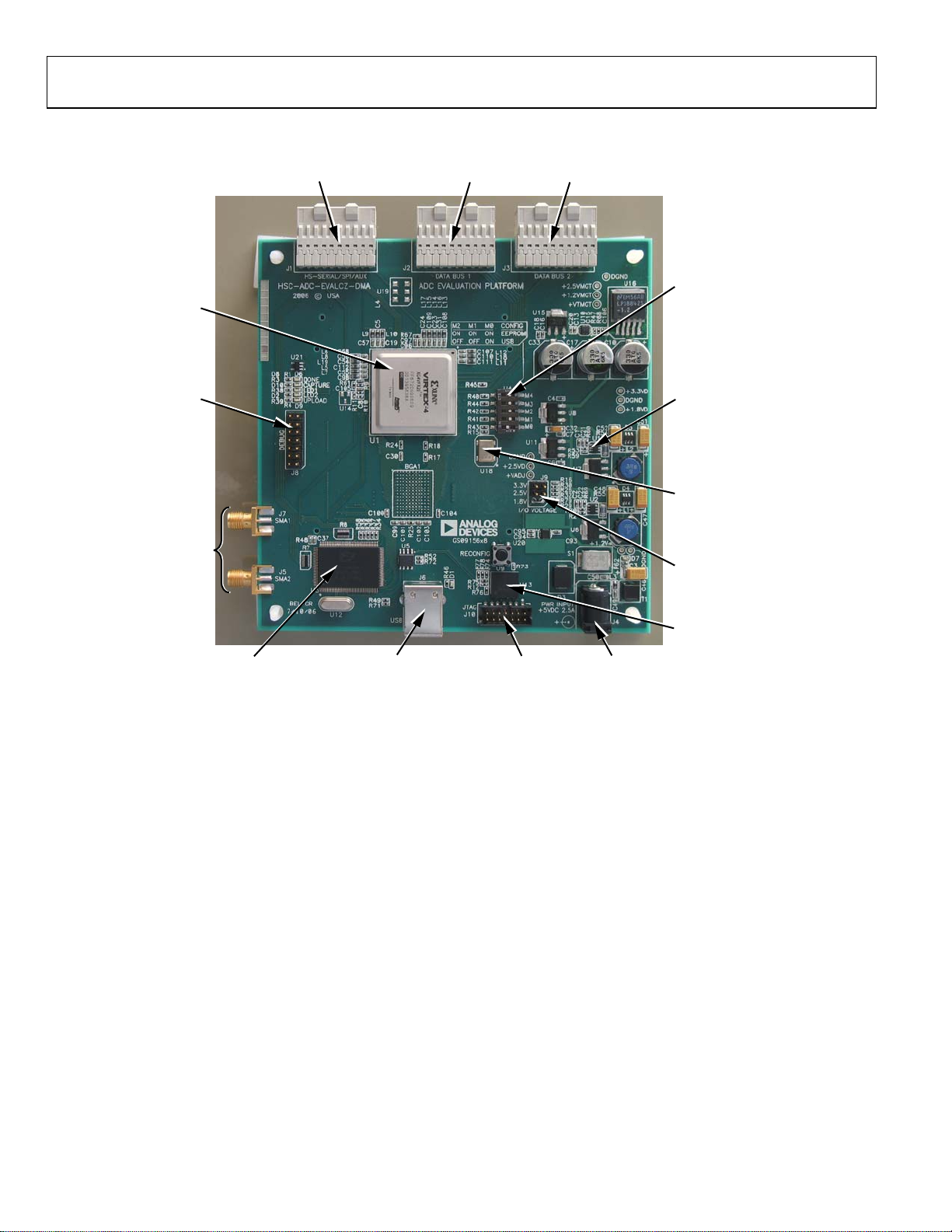
HSC-ADC-EVALC ADC CAPTURE BOARD FEATURES
GENERAL PURPOSE I/O,
USB/SPI CONTROL DATA BUS 1 DATA BUS 2
FPGA LOAD
XILINX
VIRTEX-4
FPGA
SELECT
DEBUG
PINS
EXTERNAL
SYNC I/O
CYPRESS USB
CONTROLLER
USB CONNECTOR FPGA JTAG
CONNECTOR
Figure 3. HSC-ADC-EVALC Components (Top View)
5VDC POWER
INPUT
ON BOARD
POWER SUPPLY
100MHz
OSCILLATOR
FPGA I/O
VOLTAGE MODE
FPGA CONFIG
PROM
06676-002
Rev. 0 | Page 6 of 32
Page 7
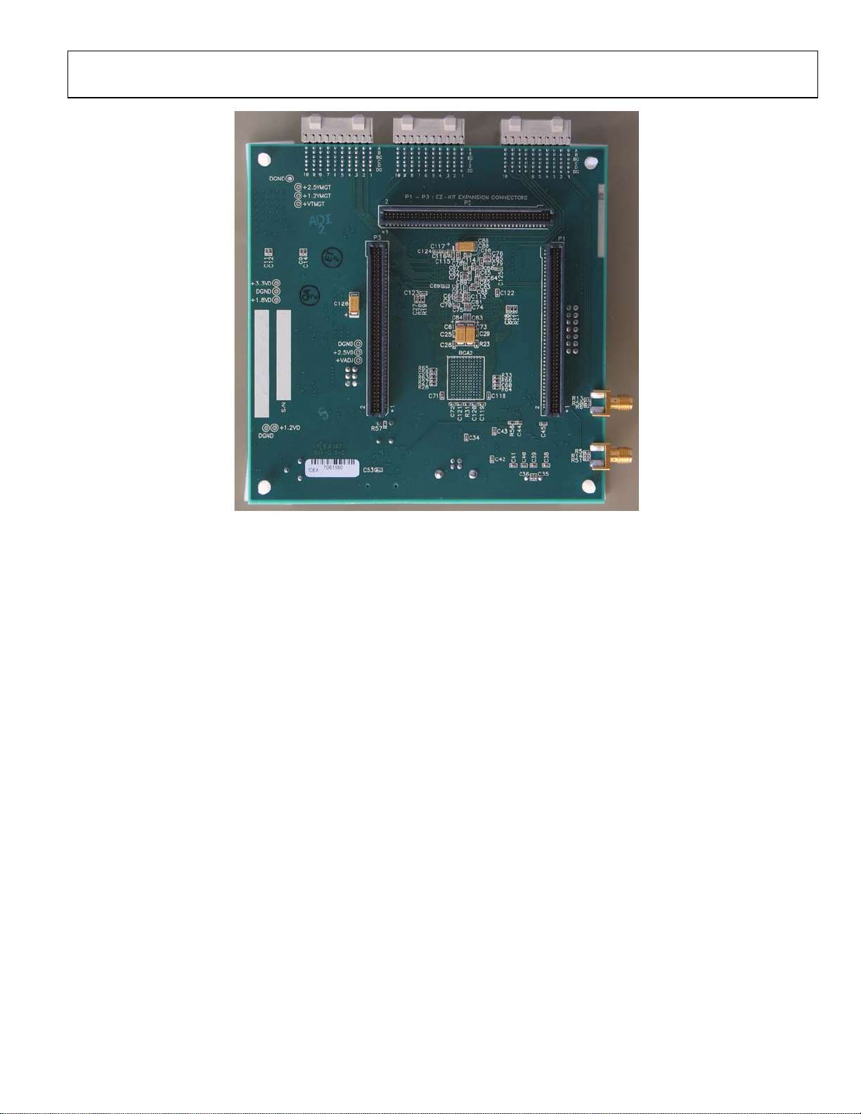
HSC-ADC-EVALC
06676-003
Figure 4. HSC-ADC-EVALC Components (Bottom View)
HSC-ADC-EVALC SUPPORTED ADC EVALUATION BOARDS
Refer to the Analog Devices ADC capture board product page at www.analog.com/FIFO for a list of HSC-ADC-EVALC-compatible ADC
evaluation boards. Some legacy ADC boards may require interposer cards to facilitate proper pin mapping to the ADC capture board. If
needed, the interposer part number is noted in the compatibility table at
www.analog.com/FIFO for the respective data converter.
Rev. 0 | Page 7 of 32
Page 8

HSC-ADC-EVALC
THEORY OF OPERATION
The HSC-ADC-EVALC evaluation platform is based around
the Virtex-4 FPGA (XC4VFX20-10FFG672C) from Xilinx®,
which can be programmed through VisualAnalog to operate
with a variety of data converters. Another key component, the
Cypress USB device (U3), communicates with a host PC and
provides the SPI interface used for configuration.
CONFIGURATION
Some converter devices require programming for mode or
feature selection, which the SPI controller accomplishes using
SPI-accessible register maps. U3 drives the 4-wire SPI (SCLK,
SDI, SDO, CSB
(J1). For more information on serial port interface (SPI) functions, consult the user manual titled Interfacing to High Speed
ADCs via SPI at
The SPI interface designed on the Cypress IC can communicate
with up to five different SPI-enabled devices including the
FPGA. The CLK and SDI/SDO data lines are common to all SPI
devices. The desired SPI-enabled device is selected for control
by using one of the five active low chip select (CS) pins. This
functionality is controlled by selecting a SPI channel in the SPI
Controller software.
At power-up, VisualAnalog attempts to autodetect the converter
that is attached to the ADC capture board using the SPI
interface. If a recognized device is found, VisualAnalog selects
the appropriate FPGA configuration; otherwise, the user is
prompted to make the device selection. In either case,
VisualAnalog then programs the FPGA using the SPI interface
of U3. The configurations typically program a FIFO data capture
function within the FPGA.
1
) signals to the converter board via connector
www.analog.com/FIFO.
INPUT CIRCUITRY
The parallel data input pins of the FPGA, which interface to the
converter, are configurable. They can operate with 1.8 V, 2.5 V,
or 3.3 V logic levels and can accept LVDS or CMOS inputs.
Each channel of the ADC capture board requires a clock signal
to capture data. These clock signals are normally provided by
the attached ADC evaluation board and are passed along with
the data through one or more pins on Connector J2 and/or
Connector J3. Refer to the HSC-ADC-EVALC I/O connector
pin mappings shown in
Figure 21 and Figure 22.
DATA CAPTURE
The process of filling the FIFO and reading the data back
requires several steps.
1. VisualAnalog initiates the FIFO fill process by resetting
the FIFOs.
2. The 48 MHz USB read clock (RCLK) is then suspended to
ensure that it does not add noise to the ADC input.
3. VisualAnalog waits approximately 30 ms to allow for data
capture before beginning the readback process. This wait
time is an adjustable parameter in VisualAnalog.
4. VisualAnalog reads the data from the FIFO through the
USB interface to the PC.
CODE DESCRIPTION
FPGA configuration files are provided by ADI for all ADCs
supported by the HSC-ADC-EVALC evaluation platform.
These files are designed and tested to facilitate quick
performance evaluations of Analog Devices data converters. No
additional FPGA programming is required from the user for
typical operation.
FPGA CONFIGURATION AND CUSTOMIZATION
Users can manually customize or update the FPGA code
through a JTAG connector (J10) provided on the ADC capture
board, as shown in
provides no support or guarantee of performance if the
provided code is customized by the user.
The HSC-ADC-EVALC hardware platform may contain additional circuit functions to support future developments and
capabilities. These functions are not supported beyond the
scope of this data sheet and the Analog Devices supplied datacapture FPGA routines at this time.
Additional FPGA programming support may be available
through the user’s local Xilinx representative or distributor.
1
Note that CSB1 is the default CSB line used.
Figure 17. However, Analog Devices
Rev. 0 | Page 8 of 32
Page 9
HSC-ADC-EVALC
EVALUATION BOARD SCHEMATICS AND ARTWORK
HSC-ADC-EVALC SCHEMATICS
TYCO AND DSP EZ–KIT CONNECTOR TO FPGA
XC4VFX20-10F FG672C XC4VFX20-10F FG672C
R50
51.1Ω
XC4VFX20-10F FG672C
R38
100Ω
Figure 5.
R39
100Ω
XC4VFX20-10F FG672C
6676-005
Rev. 0 | Page 9 of 32
Page 10
HSC-ADC-EVALC
SRAM ADDRESS AND CONTROL
R25
3.74KΩ
R27
249Ω
R28
3.74KΩ
R31
3.74KΩ
R33
249Ω
R1
100Ω
R40
3.74KΩ
R44
3.74KΩ
R42
3.74KΩ
R41
3.74KΩ
R43
3.74KΩ
U21
NC7SZ05M5X
Figure 6.
FPGA CONTROLS
XC4VFX20-10F FG672C
6676-006
Rev. 0 | Page 10 of 32
Page 11

HSC-ADC-EVALC
A
FPGA TO SRAM DAT
XC4VFX20-10F FG672C
XC4VFX20-10F FG672C
06676-007
Figure 7.
Rev. 0 | Page 11 of 32
Page 12

HSC-ADC-EVALC
A
D19 TOBE USED WITH HIGHER
DENSITY SRAM DEVICES
06676-008
Figure 8.
Rev. 0 | Page 12 of 32
Page 13

HSC-ADC-EVALC
R
SRAM AND FPGA POWE
XC4VFX20-10F FG672C
R63
499Ω
R65
499Ω
Figure 9.
R64
499Ω
R66
499Ω
XC4VFX20-10F FG672C
06676-009
Rev. 0 | Page 13 of 32
Page 14

HSC-ADC-EVALC
SRAM A BYPASS CAP
REFCLK Oscillator for IDELAYCTRL
R15
24Ω
SRAM B BYPASS CAP
FPGA BYPASS CAP
+
+
+
+
Figure 10.
06676-010
Rev. 0 | Page 14 of 32
Page 15

HSC-ADC-EVALC
UNUSED ROCKET I/0 CONNECTIONS
XC4VFX20-10F FG672C
DEBUG PINS
Figure 11.
XC4VFX20-10F FG672C
06676-011
Rev. 0 | Page 15 of 32
Page 16

HSC-ADC-EVALC
ROCKET I/0 CONNECTIONS
Figure 12.
Rev. 0 | Page 16 of 32
06676-012
Page 17

HSC-ADC-EVALC
USB CONNECTIONS
R49
R71
3.74Ω
3.74Ω
R48
100KΩ
SDI & SDO DI RECTIONS ARE WIT H
RESPECT TO T HE DEVICE UNDER
CONTROL .
Figure 13.
Rev. 0 | Page 17 of 32
(3.3V)
USB Direct I/O
06676-013
Page 18

HSC-ADC-EVALC
USB CONNECTIONS (CONTINUED)
R46
1
2
3
4
5
6
499Ω
J6
R52
3.74KΩ
R72
3.74KΩ
XC4VFX20-10F FG672C
Rev. 0 | Page 18 of 32
Figure 14.
XC4VFX20-10F FG672C
06676-014
Page 19
HSC-ADC-EVALC
EZ–KIT EXPANSION INTERFACE – FOR DSPs
P1 P2 P3
Figure 15.
06676-015
Rev. 0 | Page 19 of 32
Page 20

HSC-ADC-EVALC
J1
HS-SERIAL/SPI/AUX
06676-016
J2
DATA BUS 1
TYCO HM – Zd CONNECTORS
J3
DATA BUS 2
,
Figure 16.
Rev. 0 | Page 20 of 32
Page 21

HSC-ADC-EVALC
M
CONFIGURATION EEPRO
R77
100Ω
R78
R75
3.74KΩ
100Ω
R76
3.74KΩ
R73
ZERO
JTAG CONNECTOR EEPROM HARDWARE
RECONFIGURATION
PUSHBUTTON
R57
3.74KΩ
Figure 17.
Rev. 0 | Page 21 of 32
6676-017
Page 22
HSC-ADC-EVALC
++
+
R68
147k
+
06676-018
POWER AND VOLTAGE REGULATORS
+
+
REMOVE
DO NOT
+
TSW–102–08–G–D
+
+
Figure 18.
Rev. 0 | Page 22 of 32
Page 23
HSC-ADC-EVALC
PCB LAYOUT
GENERAL PURPOSE I/O,
USB/SPI CONTROL DATA BUS 1 DATA BUS 2
XILINX
VIRTEX-4
FPGA
FPGA LOAD
SELECT
DEBUG
PINS
EXTERNAL
SYNC I/O
CYPRESS USB
CONTROLLER
USB CONNECTO R FPGA JTAG
CONNECTOR
Figure 19. Top Silkscreen
5VDC POWER
INPUT
ON BOARD
POWER SUPPLY
100MHz
OSCILLATOR
FPGA I/O
VOLTAGE MODE
FPGA CONFIG
PROM
06676-019
Figure 20. Bottom Silkscreen
Rev. 0 | Page 23 of 32
06676-020
Page 24
HSC-ADC-EVALC
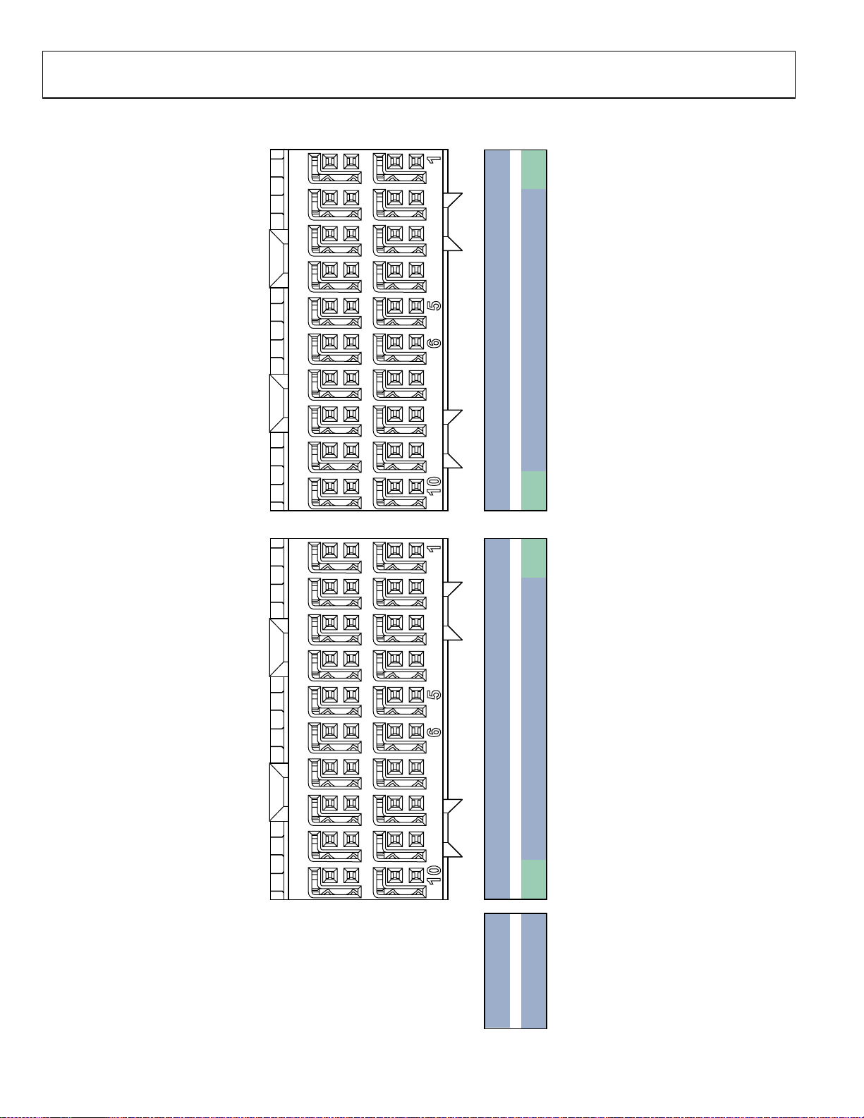
I/O CONNECTOR—J1, J2, AND J3 PIN MAPPING
D
C
B
A
DCLKB2–
D15B– D13B– D11B– D9B– D7B– D5B– D3B– D1B–
06676-021
DCLKB2+
(J2) DATA BUS 1(J3) DATA BUS 2
D15B+ D13B+ D11B+ D9B+ D7B+ D5B+ D3B+ D1B+
D17B– D16B– D14B– D12B– D10B– D8B– D6B– D4B– D2B– D0B–
D17B+ D16B+ D14B+ D12B+ D10B+ D8B+ D6B+ D4B+ D2B+ D0B+
DCLKB1–
DCLKB1+
D
C
B
A
DCLKA2–
DCLKA2+
D15A– D13A– D11A– D9A– D7A– D5A– D3A– D1A–
D15A+ D13A+ D11A+ D9A+ D7A+ D5A+ D3A+ D1A+
D17A– D16A– D14A– D12A– D10A– D8A– D6A– D4A– D2A– D0A–
D17A+ D16A+ D14A+ D12A+ D10A+ D8A+ D6A+ D4A+ D2A+ D0A+
DCLKA1–
D
C
B
A
DCLKA1+
Figure 21. J2 and J3 Pin Mapping
Rev. 0 | Page 24 of 32
LVDS DATA PATH >
CMOS/LV DS DATA PATH >
LVDS DATA PATH >
CMOS/LV DS DATA PATH >
Page 25
HSC-ADC-EVALC
m
D
C
B
A
06676-022
HIGH SPEED SE RIAL
REFERENCE CLK
HIGH SPEED SE RIAL
DATA INPUTS
FUTURE HIG H S PEED
SERIAL DATA I NP UTS
FPGA GENERAL
PURPOSE I/ O
SPI CONTRO L (3.3V)
USB DIRECT I/ O (3.3V)
D
C
B
A
MGTCLK1– SD1– SD2– SD3– SD4– SD5– SD6– SD7– SD8– MGTCLK2–
MGTCLK1+ SD1+ SD2+ SD3+ SD4+ SD5+ SD6+ SD7+ SD8+ MGTCLK2+
I/O_1 I/O_3 I/ O_5 I/O_7 SCLK SDI SDO USB_1 USB_2 USB_4
I/O_2 I/O_4 I/ O_6 I/O_8 CSB_1 CSB_2 CSB_3 CSB_4 USB_3 USB_5
(J1) HS-SERIAL/SPI/ AU X
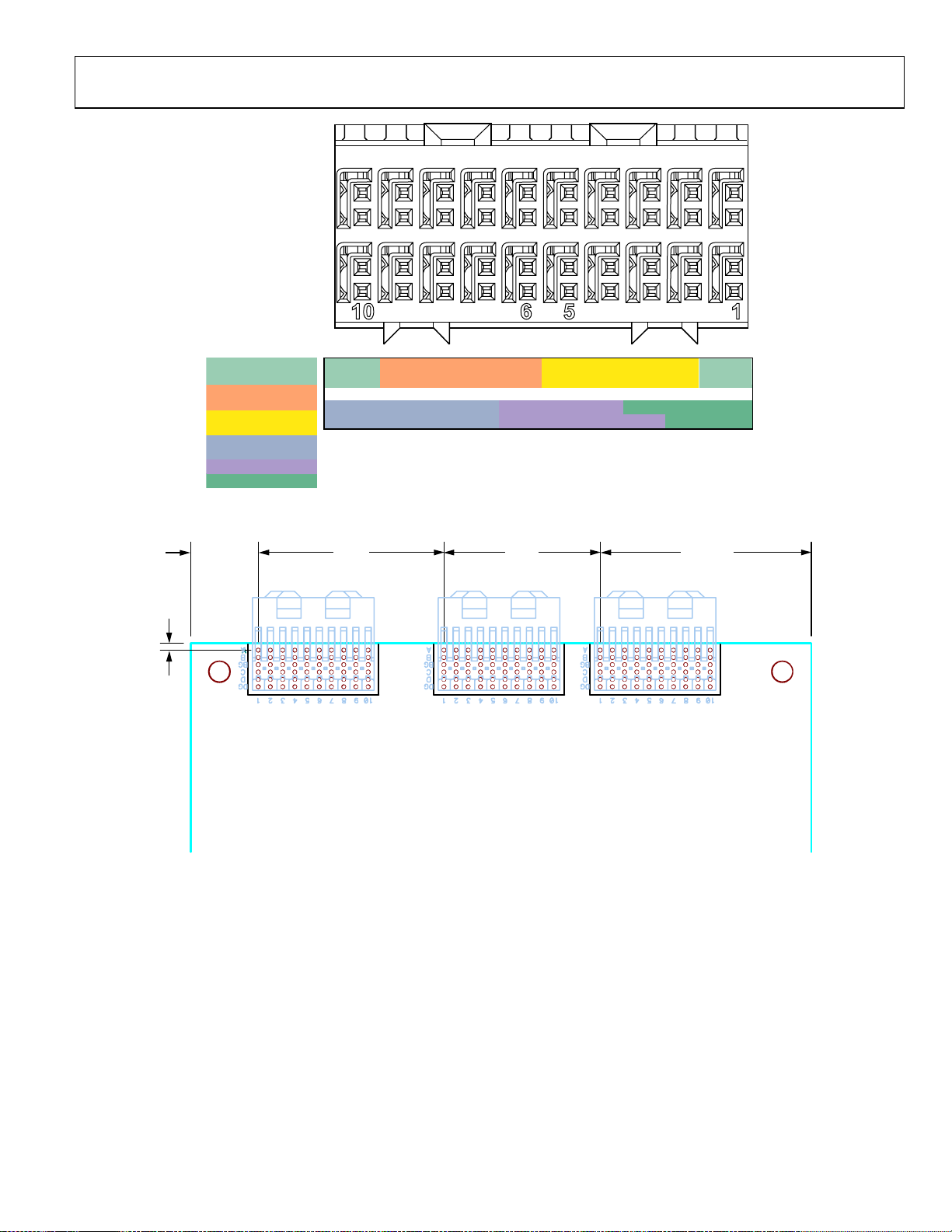
Figure 22. J1 Pin Mapping
13.843mm 38mm 32mm 43.155mm
1.4m
J1 J2
HS-SERIAL/SPI/AUX
DATA BUS 1
J3
DATA BUS 2
06676-023
Figure 23. Data Converter I/O Connector Placement (Top View)
Rev. 0 | Page 25 of 32
Page 26

HSC-ADC-EVALC
Table 3. HSC-ADC-EVALC J1 I/O Connections to FPGA (U1)
Connector J1
(HS-Serial, SPI, AUX)
A1 USB_5 none
B1 USB_4 none
C1 MGTCLK2+ AF10
D1 MGTCLK2− AF11
A2 USB_3 none
B2 USB_2 none
C2 none none
D2 none none
A3 CSB_4 none
B3 USB_1 none
C3 none none
D3 none none
A4 CSB_3 none
B4 SDO H12
C4 none none
D4 none none
A5 CSB_2 none
B5 SDI K12
C5 none none
D5 none none
A6 CSB_1 none
B6 SCLK H13
C6 SD4+ AF7
D6 SD4− AF8
A7 I/O_8 AD3
B7 I/O_7 AC3
C7 SD3+ AC1
D7 SD3− AD1
A8 I/O_6 AA3
B8 I/O_5 Y3
C8 SD2+ G1
D8 SD2− H1
A9 I/O_4 W3
B9 I/O_3 V3
C9 SD1+ A4
D9 SD1− A3
A10 I/O_2 P3
B10 I/O_1 N3
C10 MGTCLK1+ K1
D10 MGTCLK1− L1
Schematic Net Name FPGA Pin
Table 4. HSC-ADC-EVALC J2 I/O Connections to FPGA (U1)
Connector J2
(DATA BUS 1)
A1 DCLKB2+ C13
B1 DCLKB2− C12
C1 D0B+ T4
D1 D0B− T3
A2 D1B+ M4
B2 D1B− N4
C2 D2B+ P4
D2 D2B− R3
A3 D3B+ M5
B3 D3B− L5
C3 D4B+ L4
D3 D4B− L3
A4 D5B+ K3
B4 D5B− J3
C4 D6B+ L7
D4 D6B− M6
A5 D7B+ J4
B5 D7B− H3
C5 D8B+ K6
D5 D8B− J5
A6 D9B+ G5
B6 D9B− F4
C6 D10B+ H4
D6 D10B− G4
A7 D11B+ H8
B7 D11B− H7
C7 D12B+ G7
D7 D12B− H6
A8 D13B+ F8
B8 D13B− F7
C8 D14B+ K8
D8 D14B− K7
A9 D15B+ B9
B9 D15B− A9
C9 D16B+ A8
D9 D16B− A7
A10 DCLKB1+ A12
B10 DCLKB1− B12
C10 D17B+ B10
D10 D17B− A10
Schematic Net Name FPGA Pin
Rev. 0 | Page 26 of 32
Page 27

HSC-ADC-EVALC
Table 5. HSC-ADC-EVALC J3 I/O Connections to FPGA (U1)
Connector J3
(DATA BUS 2)
A1 DCLKA2+ C14
B1 DCLKA2− B14
C1 D0A+ D6
D1 D0A− E6
A2 D1A+ H9
B2 D1A− G9
C2 D2A+ E8
D2 D2A− E7
A3 D3A+ L10
B3 D3A− L9
C3 D4A+ J9
D3 D4A− K10
A4 D5A+ C3
B4 D5A− D3
C4 D6A+ E3
D4 D6A− F3
A5 D7A+ D5
B5 D7A− E5
C5 D8A+ C4
D5 D8A− D4
A6 D9A+ B7
B6 D9A− C7
C6 D10A+ B6
D6 D10A− C6
A7 D11A+ D9
B7 D11A− C9
C7 D12A+ D8
D7 D12A− C8
A8 D13A+ C11
B8 D13A− B11
C8 D14A+ E10
D8 D14A− D10
A9 D15A+ G10
B9 D15A− F10
C9 D16A+ E11
D9 D16A− D11
A10 DCLKA1+ A14
B10 DCLKA1− A13
C10 D17A+ G12
D10 D17A− G11
Schematic Net Name FPGA Pin
Rev. 0 | Page 27 of 32
Page 28

HSC-ADC-EVALC
ORDERING INFORMATION
BILL OF MATERIALS (RoHS COMPLIANT)
Table 6.
Qty Reference Designator Description Manufacturer Part Number
1 PCB PCB, ADC evaluation platform MOOG/PCSM GS09156x8
0 BGA1, BGA2
2 C1, C2
3 C10, C17, C33 Capacitor, 330 μF, 10 V TG SMD Panasonic/ECG EEETG1A331P
2 C21, C22
67
C3, C25 to C30, C34,
C37 to C45, C59, C60,
C63 to C72, C74 to
C76, C78 to C85, C88
to C92, C96 to C98,
C100 to C106, C113 to
C118, C120 to C125
1 C32
2 C35, C36
18
C4, C6, C7, C9, C11 to
C14, C16, C18, C20,
C62, C77, C87, C93,
C95, C99, C119
7
C46, C48, C52, C61,
C73, C86, C126
2 C47, C51 Capacitor, 47 μF, 10 V, tantalum TEL SMD Epcos, Inc. B45197A2476K309
2 C49, C50
17
C5, C19, C23, C24, C31,
C53 to C58, C107 to
C112
1 C94
7 D1, D2, D6 to D10 LED green, clear lens SMD Panasonic LNJ308G8TRA
1 D3 PolySwitch surface-mount (PTC devices) International IRF Rectifiers 30BQ015TRPBF
2 D4, D5
1 J1, J2, J3
1 J10
1 J4 Connector, DC power jack CUI Inc. PJ-102AH
1 J6 Connector, USB Type B Mill-Max 897-43-004-90-000000
2 J5,J7
1 J8
1 J9 (2.5 V and 3.3 V) Connector, 2 × 2 header, 100 mil Samtec, Inc. TSW-102-08-G-D
1
J9 (Jumper Pin 1 to
Jumper Pin 2)
1 L1 Inductor, 4.6 μH SMD, Code 0004 Sumida CDR7D28MN4R6
1 L2 Inductor, 3.6 μH SMD, Code 0003 Sumida CDR7D28MN3R6
IC, 18-bit DDRII SRAM 2-word burst
operation (MOS integrated circuit),
do not install
Capacitor, 470 pF, 50 V ceramic
X7R 0402
Capacitor, 68 pF, 50 V, ceramic
0402 SMD
Capacitor, 0.1 μF, 10 V, ceramic
X5R 0402
Capacitor, 10 μF, 6.3 V, tantalum
TE series
Capacitor, 12 pF, 50 V, ceramic
0402 SMD
Capacitor, 0402 chip, X5R, 6.3 V,
1 μF, ± 20%
Capacitor, 10 μF, 20 V, tantalum TEL SMD AVX TPSC106K025R0500
Capacitor, 1000 pF, 50 V, ceramic Y5V
0402
Capacitor, 0402 chip, X5R, 6.3 V,
0.22 μF, ±10%
Capacitor, 470 pF, 25 V, ceramic
0402 SMD
40 V silicon high current Schottky
barrier diode
Connector, 2-pair 10 column high speed
HM-Zd PCB mount
Connector, 2 mm, 2 × 7 pin SMT vertical
male, with shroud
Connector, end launch jack/PCB, 62 mil,
gold
Connector, 25 mil square postheader,
100 mil, 2 × 7
Solder wire jumper (Pin 1 indicator to
1.8 V on silkscreen)
Rev. 0 | Page 28 of 32
NEC PD44164362F5-EQ1
Panasonic/ECG ECJ-0EB1H471K
Panasonic/ECG ECU-E1H680JCQ
Panasonic/ECG ECJ-0EB1A104K
Kemet T491A106M006AT
Panasonic/ECG ECJ-0EC1H120J
Panasonic ECJ-0EB0J105M
Panasonic/ECG ECJ-0EF1H102Z
Panasonic ECJ-0EB0J224K
Panasonic/ECG ECJ-0EB1E471K
Zetex Semiconductors ZHCS2000
Tyco 6469028-1
Molex 87832-1420-TB32
Emerson 142-0701-801
Samtec, Inc. TSW-107-08-G-D
Page 29

HSC-ADC-EVALC
Qty Reference Designator Description Manufacturer Part Number
17 L3 to L19 Ferrite chip, 220 Ω, 2 A, 0603, 100 MHz TDK MPZ1608S221A
3 P1 to P3
13
R1, R3, R4, R34 to R39,
R61, R67, R77, R78
3 R15, R56, R74 Resistor, 24 Ω, 1/16 W, 5%, 0402 SMD Panasonic/ECG ERJ-2GEJ240X
1 R16 Resistor, 75 kΩ, 1/16 W, 1%, 0402 SMD Panasonic/ECG ERJ-2RKF7502X
5 R17, R18, R23, R24, R50 Resistor, 51.1 Ω, 1/16 W, 1%, 0402 SMD Panasonic/ECG ERJ-2RKF51R1X
10
R19 to R22, R46, R62 to
R66
1 R2 Resistor, 40.2 kΩ, 1/16 W, 1%, 0402 SMD Panasonic/ECG ERJ-2RKF4022X
17
R25, R28, R31, R40 to
R45, R49, R52, R57,
R58, R71, R72, R75, R76
1 R26 Resistor, 169 kΩ, 1/16 W, 1%, 0402 SMD Panasonic/ECG ERJ-2RKF1693X
2 R27, R33 Resistor, 249 Ω, 1/16 W, 1%, 0402 SMD Panasonic/ECG ERJ-2RKF2490X
1 R68 Resistor, 147 kΩ, 1/16 W, 1%, 0402 SMD Panasonic/ECG ERJ-2RKF1473X
1 R29 Resistor, 226 kΩ, 1/16 W, 1%, 0402 SMD Panasonic/ECG ERJ-2RKF2263X
0 R30
1 (R32), R79
1 R47 Resistor, 76.8 kΩ, 1/16 W, 1%, 0402 SMD Panasonic/ECG ERJ-2RKF7682X
2 R48, R59 Resistor, 100 kΩ, 1/16 W, 1%, 0402 SMD Panasonic/ECG ERJ-2RKF1003X
3 R5, R6, R73 Resistor 0 Ω, 1/16 W, 5%, 0402 SMD Panasonic/ECG ERJ-2GE0R00X
2 R53, R70 Resistor 80.6 kΩ, 1/16 W, 1%, 0402 SMD Panasonic/ECG ERJ-2RKF8062X
1 R54 Resistor, low value, 1206 SMD, 0.04 Ω TT Electronics LRC-LR1206LF-01-R040-F
1 R55 Resistor, low value, 1206 SMD, 0.06 Ω TT Electronics LRC-LR1206LF-01-R060-F
2 R60, R69 Resistor, 25.5K Ω, 1/16 W, 1%, 0402 SMD Panasonic/ECG ERJ-2RKF2552X
2 R7, R8 Resistor array network, 8 Ω to 22 Ω chip Panasonic EXB-2HV220JV
1 S1 Fuse, PolySwitch SMT (PTC devices) Tyco SMD250F-2
1 T1
1 U1 Virtex-4 FPGA Xilinx XC4VFX20-10FFG672C
2 U10, U20
2 U11, U15
1 U12 Crystal oscillator, 24 Mhz, 12 pF, SMD ECS ECS-240-12-4X
1 U13 1.8 V, 8 Mb, platform flash-in system Xilinx XCF08PFSG48C
1 U16
1 U18
0 U19
2 U2, U17
1 U21
1 U3 IC, EZ-USB FX2LP USB microcontroller Cypress Semiconductor Corp. CY7C68013A-128AXC
1 U4 Switch, 5-position, SMT, DIP CTS 219-5MST
1 U5 IC, 128-bit I2C bus serial EEPROM Microchip 24LC00-I/SN
Connector, 0.050 in × 0.050 in, Samtec
TFM series, 2R
Resistor, 100 Ω, 1/16 W, 1%, 0402 SMD Panasonic/ECG ERJ-2RKF1000X
Resistor, 499 Ω, 1/16 W, 1%, 0402 SMD Panasonic/ECG ERJ-2RKF4990X
Resistor, 3.74 kΩ, 1/16 W, 1%, 0402 SMD Panasonic/ECG ERJ-2RKF3741X
Resistor, 140 kΩ, 1/16 W, 1%, 0402 SMD,
do not install
Resistor, 107 kΩ, 1/16 W, 1%, 0402 SMD,
do not install R32
Choke, common-mode coils, wirewound type for large current
DLW5AH/DLW5BS series
(2014/2020 Size)
Voltage regulator, high accuracy, low IQ,
adjustable
Voltage regulator, high accuracy
ultralow IQ, 1.5 A
Voltage regulator, 1.5 A ultralow
dropout linear regulator
Crystal controlled oscillator (100 MHz
fixed frequency oscillator)
156.25 MHz low jitter saw crystal
oscillator, do not install
IC, constant frequency current-mode,
step-down, dc-to-dc controller in TSOT
IC, single inverter buffer/driver with
open-drain output
Samtec, Inc. TFM-145-32-S-D-A
Panasonic/ECG ERJ-2RKF1403X
Panasonic/ECG ERJ-2RKF1073X
Murata DLW5BSN191SQ2
Analog Devices ADP3334ACPZ-REEL7
Analog Devices ADP3339AKCZ-2.5R7
National Semiconductor LP38842S-1.2
Connor-Winfield Corp. CWX823-100.0M
Epson Electronics America EG-2121CA 156.2500M-PHPAL3
Analog Devices ADP1864AUJZ-R7
Fairchild Semiconductor NC7SZ05M5X
Rev. 0 | Page 29 of 32
Page 30

HSC-ADC-EVALC
Qty Reference Designator Description Manufacturer Part Number
2 U6, U7
1 U8
1 U9 Switch, 6 mm light touch SW, N.O. Alps SKHHAKA010
4 H1, H2, H3, H4 Circuit board support on base Richco, Inc. CBSB-14-01
1 Packed with PCB Transformer 5 V, 3 A switcher P5 CUI, Inc. DPS050300U-P5P-TK
0 U14
0 R9
0 R12, R13, R14, R51
0 R11
0 R10
0 C8
0 C15
IC, P-channel enhancement mode field
effect transistor
Voltage regulator, high accuracy
ultralow IQ, 1.5 A
1.2 V precision low noise shunt voltage
references, SOT-23 (RT-3), do not install
Resistor, 6.2 kΩ, 1/16 W, 5%, 0402 SMD,
do not install
Resistor, 0 Ω, 1/16 W, 5%, 0402 SMD,
do not install
Resistor 13 k Ω, 1/16 W, 5%, 0402 SMD,
do not install
Resistor 1.0 kΩ, 1/16 W, 5%, 0402 SMD,
do not install
Capacitor, 0402 SMD, X5R, 6.3 V, 0.22 μF,
±10%, do not install
0402 chip capacitor, X5R, 6.3 V, 1 μF,
±20%, do not install
Fairchild Semiconductor NDT456P
Analog Devices ADP3339AKCZ-3.3
Analog Devices ADR512ART
Panasonic/ECG ERJ-2GEJ622X
Panasonic/ECG ERJ-2GE0R00X
Panasonic/ECG ERJ-2GEJ133X
Panasonic/ECG ERJ-2GEJ102X
Panasonic ECJ-0EB0J224K
Panasonic ECJ-0EB0J105M
ORDERING GUIDE
Model Description
HSC-ADC-EVALC Data Converter Evaluation Platform
HSC-ADC-EVALCZ1 Data Converter Evaluation Platform
1
Z = RoHS Compliant Part.
ESD CAUTION
Rev. 0 | Page 30 of 32
Page 31

HSC-ADC-EVALC
NOTES
Rev. 0 | Page 31 of 32
Page 32

HSC-ADC-EVALC
NOTES
©2007 Analog Devices, Inc. All rights reserved. Trademarks and
registered trademarks are the property of their respective owners.
EB06676-0-4/07(0)
Rev. 0 | Page 32 of 32
 Loading...