

查询EVAL-ADF4213EB2供应商查询EVAL-ADF4213EB2供应商
2.35GHz Dual Evaluation Board For
=
FEATURES
Self-Contained Board including Synthesizer, RF VCO and
loop filter for generating frequencies of 2.3GHz to
2.4GHz and IF VCO and loop filter for generating fre-
quencies of 700MHz to 850MHz
Designed for 20kHz Loop Bandwidth
Accompanying Software allows complete control of synthesizer
functions from PC using Windows 95/98/NT
Battery Operated: Choice of 3V or 5V supplies
On Board Monitoring of Current and Voltage.
Typical Phase Noise Performance of -83.5dBc/Hz (RF side)
@ 1kHz offset
Typical Phase Noise Performance of -90dBc/Hz (IF side) @
1kHz offset.
BLOCK DIAGRAM
9V BATTERY
V
DD
9V BATTERY
PLL Frequency Synthesizer
EV AL-ADF4213EB2
GENERAL DESCRIPTION
This board is designed to allow the user to evaluate
the performance of the ADF4213 Dual Frequency
Synthesizer for PLL's (Phase Locked Loops). The
block diagram of the board is shown below. It contains the ADF4213 synthesizer, a pc connector, SMA
connector for the reference input, power supplies and
RF and IF output. There is also a loop filter for both
sides (20kHz bandwidth) and an RF and IF VCO on
board. A cable is included with the board to connect
to a pc printer port.
The package also contains windows software to allow
easy programming of the synthesizer.
V
VCO
VCO1
VTUN
VCO1
FOUT
RF
OUT
REF
IN
VCO 1
(Va ri-L )
VCO 190-2350T
SMA
Socket
TCXO
Vectron 19M2
EVAL-ADF4213EB2
PC CONNECTOR
PC CONNECTOR
POWER SW ITCH
ON OFF
ADF4213
VCO 190-775T
AD7706
AD7706
VCO 2
(Va ri-L )
SMA
Socket
V
P
VCO2
VTUN
VCO2
FOUT
IF
RSET
OUT
REV.PrA 01/00
Information furnished by Analog Devices is believed to be accurate and reliable.
However, no responsibility is assumed by Analog Devices for its use, nor for any
infringements of patents or other rights of third parties which may result from its use.
No license is granted by implication or otherwise under any patent or patent rights of
Analog Devices.
© Analog Devices, Inc., 1999
One Technology Way, P.O. Box 9106, Norwood, MA 02062-9106, U.S.A.
Tel: 781-329-4700 Fax: 781-326-8703
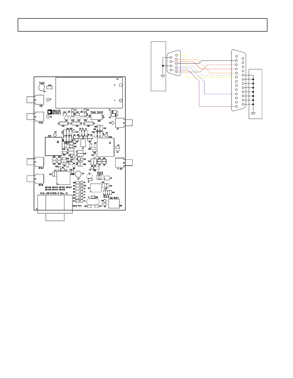
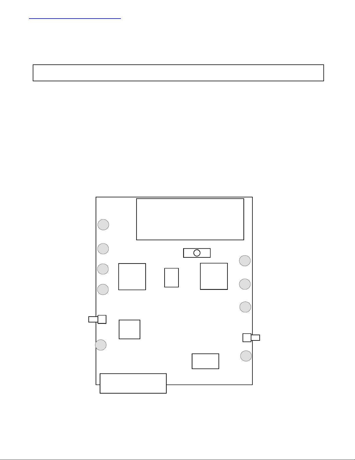
Hardware Description
The evaluation board comes with a cable for connecting to
the printer port of a PC. The silk screen and cable diagram for
the evaluation board are shown below. The board schematic is
shown on pages 3 and 4.
EV AL-ADF4213EB2
EVAL-ADF411X
EVAL-ADF421X
1
6
2
7
3
8
4
9
5
9 Way
Female D-Type
To
ADF411X
ADF421X
Evaluation
Board
Brown - DATA
Figure 2. PC Cable Diagram
This helps the user pick the optimum synthesizer settings
for power consumption and also provides an alert if the
battery voltage is too low to sustain the required 3V or 5V
for the board supply.
The RF loop component values are for a 2.35GHz output,
with 5mA CP current, VCO 190-2350T, 200kHz channel
spacing and 20kHz loop band-width.
The component values for the IF side are for a 760MHz
output, 5mA CP current, VCO190-775T, 200kHz channel spacing and 20kHz loop band-width.
Black - CLK
Red - LE
Orange - CE
White - GND
Yellow
Purple
1
2
3
4
5
6
7
8
9
10
Blue
11
12
13
25 Way Male
D-Type
To
PC Printer Port
14
15
16
17
18
19
20
21
22
23
24
25
PC
Figure 1. Evaluation Board Silkscreen
The board is powered from a single 9V battery. The
power supply ciruitry allows the user to choose either 3V
or 5V for the ADF4213 V
supply. The default settings are 3V for the ADF4213 V
and VP, and for the VCO
DD
DD
and 5V for the ADF4213 VP and for the VCO supply. It
is very important to note that the ADF4213 V
never exceed the ADF4213 V
. This can damage the de-
P
should
DD
vice.
All components necessary for LO generation are onboard. The 19.2 MHz TCXO from Vectron provides the
necessary Reference Input. The PLL on the RF side is
made up of the ADF4213, passive loop filter (20kHz
bandwidth) and the VCO 190-2350 from Vari-L. The
PLL on the IF consistes of the ADF4213, passive loop
filter (20kHz bandwidth) and the VCO 190-775. The
respective outputs are available at RFOUTand IFOUT
through standard SMA connectors. If the user wishes they
may use their own power supplies and reference input. In
this case, they need to insert SMA connectors to as shown
on the silkscreen and block diagram.
The AD7706 A/D converter is used to monitor the power
supply voltage and current consumption of the ADF4213.
–2–
REV.PrA 01/00
EVAL-ADF4213EB2
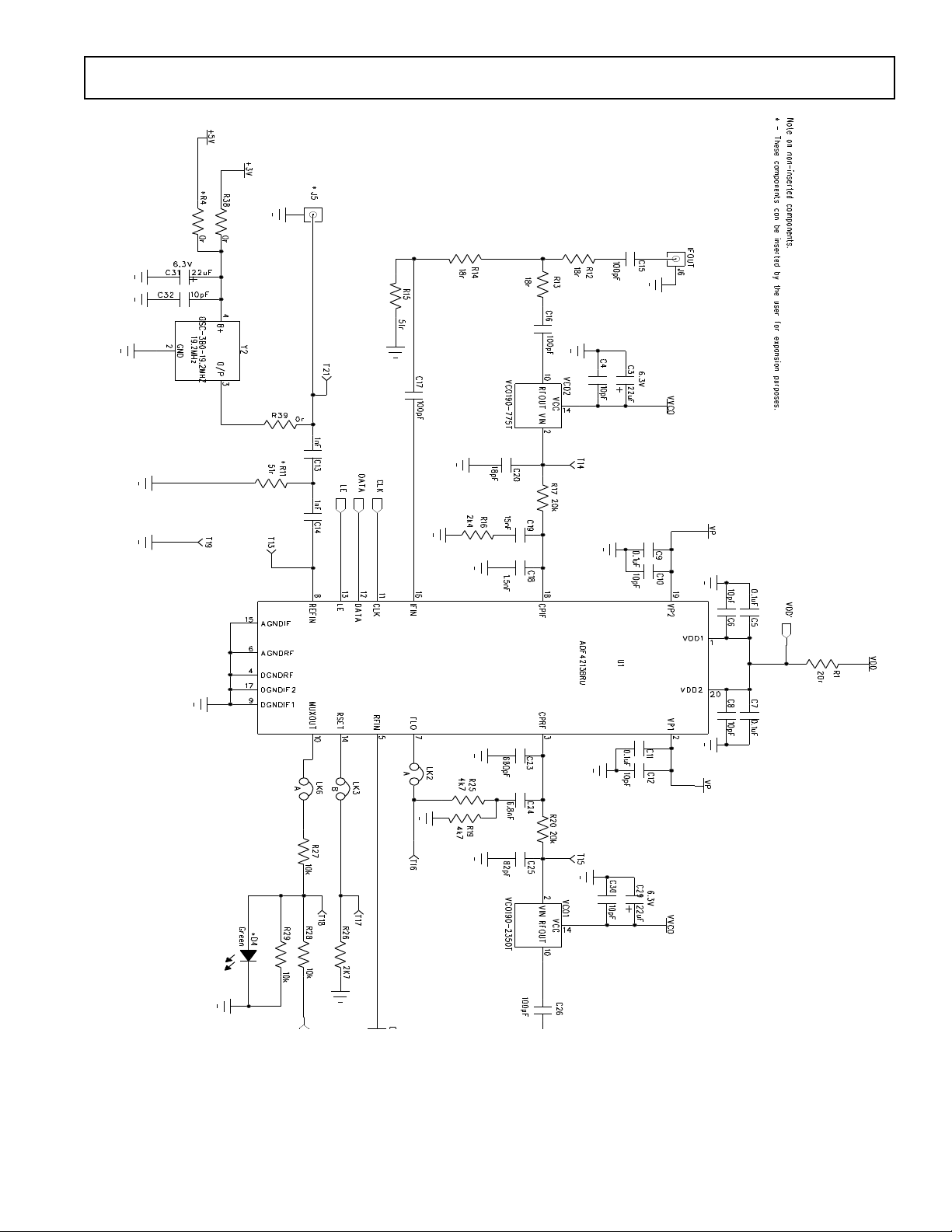
Figure 3. Evaluation Board Circuit Diagram (Page 1)
–3–
REV.PrA 01/00

EV AL-ADF4213EB2
Figure 4. Evaluation Board Circuit Diagram (Page 2)
–4–
REV.PrA 01/00

Software Description
The software comes on a CD. If the user runs
“ADF4XXXEvaluationSoftware.exe” on the CD, then the
install wizard installs the software. Follow the on-screen
directions. The software will be installed in a default
directory called “C:\Program Files\Analog
Devices\ADF4xxx Evaluation Software”. To run the
software, simply double click on "ADF4XXX Eval
Software.exe".
The front panel of the evaluation board software is shown
below.
When the main software screen appears, follow the steps
below for initial setup to interface to the part.
Click on Choose Device, and the Device window will
appear. Choose the ADF4213 and click OK.
The settings for this Evaluation Board are saved under
options and presets. Select EVAL-ADF4213EB2. To
manually configure the settings do the following:
EVAL-ADF4213EB2
Click on the value on the front page to bring up a
submenu. Change the value of the parameter. Click the
OK button. Use this to change the output frequency, PFD
Frequency, Reference Input etc.
The Evaluation board feaures an A/D converter whcih
allows the volatges supplied and current drawn by the part
to be displayed on screen. Press the "Update Voltage and
Current Supply" readback these values.
Figure 5. Software Front Panel
–5–
REV.PrA 01/00

EV AL-ADF4213EB2
y
y
y
y
y
y
y
y
y
y
y
y
y
y
y
y
gg
g
g
y
y
y
Qty Reference Description Manufacturer PCB DECAL VALUE
1 U1 ADF 421 3BRU ADI TSSOP-20 ADF 421 3BRU
1 U2 AD7706BR ADI SO16WB AD7706BR
1 U3 AD780AR ADI SO8NB AD780AR
1 U4 ADP3300ART-5 ADI SOT23-6 ADP3300ART-5
1 U5 ADP3300ART-3 ADI SOT23-6 ADP3300ART-3
1 VCO 1 2350MHz VCO Vari-L VCO 190-2350T
1 VCO 2 775MHz V C O Vari-L VCO 190-775T
1 Y1 4. 9152M Hz Cr
1Y2 19.2 MHz TCXO
1 D1 SD103C S chottk
1 D2 IN4001 D035 FE C 365-117
1 D3 Red Low Po wer LE D Vis ha
1 D4 Green Low P ower LE D (Do Not Inse rt) V isha
stal
Diode General S em ic on duc t or DO35 SD103C
Vectron International
Vectron International
HC49 low profile VXA1-1011
OS C-3B0-19.2MHZ
LED FE C 657-130
LED FE C 657-141
6 C1 C5 C7 C9 C11 C41 Mu lt i La
1 C2 Tantalum Capacitor AV X CAP \ TAJ_B 10uF 6. 3V
3 C3 C29 C31 Tantalum Ca pac it or AV X CAP \ TAJ_A 22uF 6. 3V
7 C4 C6 C8 C10 C12 C30 C32 Mult i La
2 C13-14 Multi La
6 C15-17 C26-28 Multi La
1 C18 Multi La
1 C19 Multi La
1 C20 Multi La
2 C21-22 Multi La
1 C23 Multi La
1 C24 Multi La
1 C25 Multi La
3 C33 C36 C40 Mult i La
2 C34 C37 Tantalum Capacitor AV X CAP \ TAJ_A 1uF 16V
2 C35 C38 Tantalum Capacitor AV X CAP \ TAJ_A 4.7uF 1 0V
2 C39 C42 Tantalum Capacitor AV X CAP \ TAJ_A 10uF 6. 3V
1 R1 Resis t or (Su rface M ount ) Bourns Case 0805 20r 1.0%
7 R2 R5-10 Resis t or (S urface M ount ) Bourns Case 0 603 330r 1.0%
1 R3 Resis t or (Su rface M ount ) Bourns Case 0603 3k 3 1.0 %
1 R4 Do Not Insert Bourns Case 0603
1 R11 Do Not Insert Bourns Case 0603
6 R12-14 R21-23 Resistor (Surface Mount) Bourns Case 0603 18r 1.0%
2 R15 R24 Resis t or (S urface M ount ) Bourns Case 0 603 51r 1.0%
1 R16 Res is t or (Surface M o unt) Bo urns Ca s e 0805 2k4 1. 0%
1 R17 Resis tor (Surface Mount) Bourns Case 0805 20k 1.0%
1 R18 Resis tor (Surface Mount) Bourns Case 0603 1M 1.0%
1 R19 Res is t or (Surface M o unt) Bo urns Ca s e 0805 4k7 1. 0%
1 R20 Resis tor (Surface Mount) Bourns Case 0805 20k 1.0%
1 R25 Res is t or (Surface M o unt) Bo urns Ca s e 0805 4k7 1. 0%
1 R26 Res is t or (Surface M o unt) Bo urns Ca s e 0603 2k7 1. 0%
3 R27-29 Resist or (Surface Mount) B ourns Case 0603 10k 1.0%
6 R30-33 R40-41 Resistor (Surface Mount) Me
2 R34-35 Res is t or (Su rface M ount ) B o urns Ca s e 0603 0r 1.0%
2 R36 R37 Resis t or (Su rface M ount ) Bourns Case 0603 330k 1. 0%
2 R38 R39 Resis t or (Su rface M ount ) Bourns Case 0603 0r 1.0%
1 R42 Res is t or (Surface M o unt) Bo urns Ca s e 0603 4k7 1. 0%
er Ceramic Capac i tor Murata Case 0603 0.1uF
er Ceramic Capac i tor Murata Case 0603 10pF
er Ceramic Capac i tor Murata Case 0603 1nF
er Ceramic Capac i tor Murata Case 0603 100pF
er Ceramic Capac i tor Murata Case 0805 1.5nF
er Ceramic Capac i tor Murata Case 0805 15nF
er Ceramic Capac i tor Murata Case 0805 18pF
er Ceramic Capac i tor Murata Case 0603 33pF
er Ceramic Capac i tor Murata Case 0805 680pF
er Ceramic Capac i tor Murata Case 0805 6.8nF
er Ceramic Capac i tor Murata Case 0805 82pF
er Ceramic Capac i tor Murata Case 0603 10nF
itt Ca s e 0603 100k 0. 1%
1 SW1 Pus h Button S wi tc h Om ron S W\P B-SM A LL FE C 176-986
1 SW2 SP DT Swi tch - (Was habl e) Apem SW_SIP-3P FEC 150-559
21 T1-21 Red Testpoi nt W Hu
1 J1 9 PIN D-TYPE MALE (HO RIZ) Mc M urdo DCON9M F E C 15 0-750
4 J2 J3 J4 J5 J6 Do No t Insert SMA
2 J6 J7 GOLD 50Ω SM A SOCKE T P a s ternac k SM A PE 4118
3 LK1 LK 4 LK5 3 pin header Harwin S IP -3P FE C 512-047
3 LK2-A LK 3-B LK 6-A Wi re link
3 LK1 LK 4 LK5 Shortin
4 Eac h C orner Rubber St ic k-On Feet 3M FE C 148-922
2 P1 P air P CB s n ap-on bat ter
1 P1 9V PP3 Batter
1 P CB EV A L-ADF4 21 XEB -5 (Re v. A )
Parts Free issued b
Leave pos iti on blank - Do not in s ert.
ADI.
Shunt Harwin FE C 150-410
connec t or Keysto ne BATT_PP3 FEC 723-988
–6–
hes TESTPOINT FE C-240-345
Duracell FE C 908-526
REV.PrA 01/00
 Loading...