

查询EVAL-ADF4208EB1供应商查询EVAL-ADF4208EB1供应商
Evaluation Board For PLL Frequency
=
FEATURES
Evaluation Board featuring the ADF4208 synthesiser.
Requires only RF and IF VCO's and Loop Filters for dual
PLL.
Complete with SMA connectors, battery, and on board
10MHz Crystal.
Programmable via a serial interface.
Accompanying Software allows complete control of synthesizer
functions from PC using Windows 95/98/NT
Battery Operated: Choice of 3V or 5V supplies
On Board Monitoring of Current and Voltage.
BLOCK DIAGRAM
9V BATTERY
V
DD
9V BATTERY
Synthesizer
EV AL-ADF4208EB1
GENERAL DESCRIPTION
This board is designed to allow the user to evaluate
the performance of the ADF4208 Dual Frequency
Synthesizer for PLL's (Phase Locked Loops). The
block diagram of the board is shown below. It contains the ADF4208 synthesizer, a pc connector, and
SMA connections for refererence input, power
supplies and RF and IF output. The board only
requires an RF VCO and loop filter and an IF VCO
and loop filter. A cable is included with the board to
connect to a pc printer port.
The package also contains windows software to allow
easy programming of the synthesizer.
V
VCO
VCO1
VTUN
VCO1
FOUT
RF
OUT
REF
IN
VCO 1
No t Pop u la te d
SMA
Socket
10 MHz Crystal
EVAL-ADF4208EB1
PC CONNECTOR
PC CONNECTOR
POWER SW ITCH
ON OFF
ADF4208
No t Pop u la ted
AD7706
AD7706
VCO 2
SMA
Socket
V
P
VCO2
VTUN
VCO2
FOUT
IF
RSET
OUT
REV.PrA 02/00
Information furnished by Analog Devices is believed to be accurate and reliable. However,
no responsibility is assumed by Analog Devices for its use, nor for any infringements of
patents or other rights of third parties which may result from its use. No license is granted
by implication or otherwise under any patent or patent rights of Analog Devices.
© Analog Devices, Inc., 1999
One Technology Way, P.O. Box 9106, Norwood, MA 02062-9106, U.S.A.
Tel: 781-329-4700 Fax: 781-326-8703
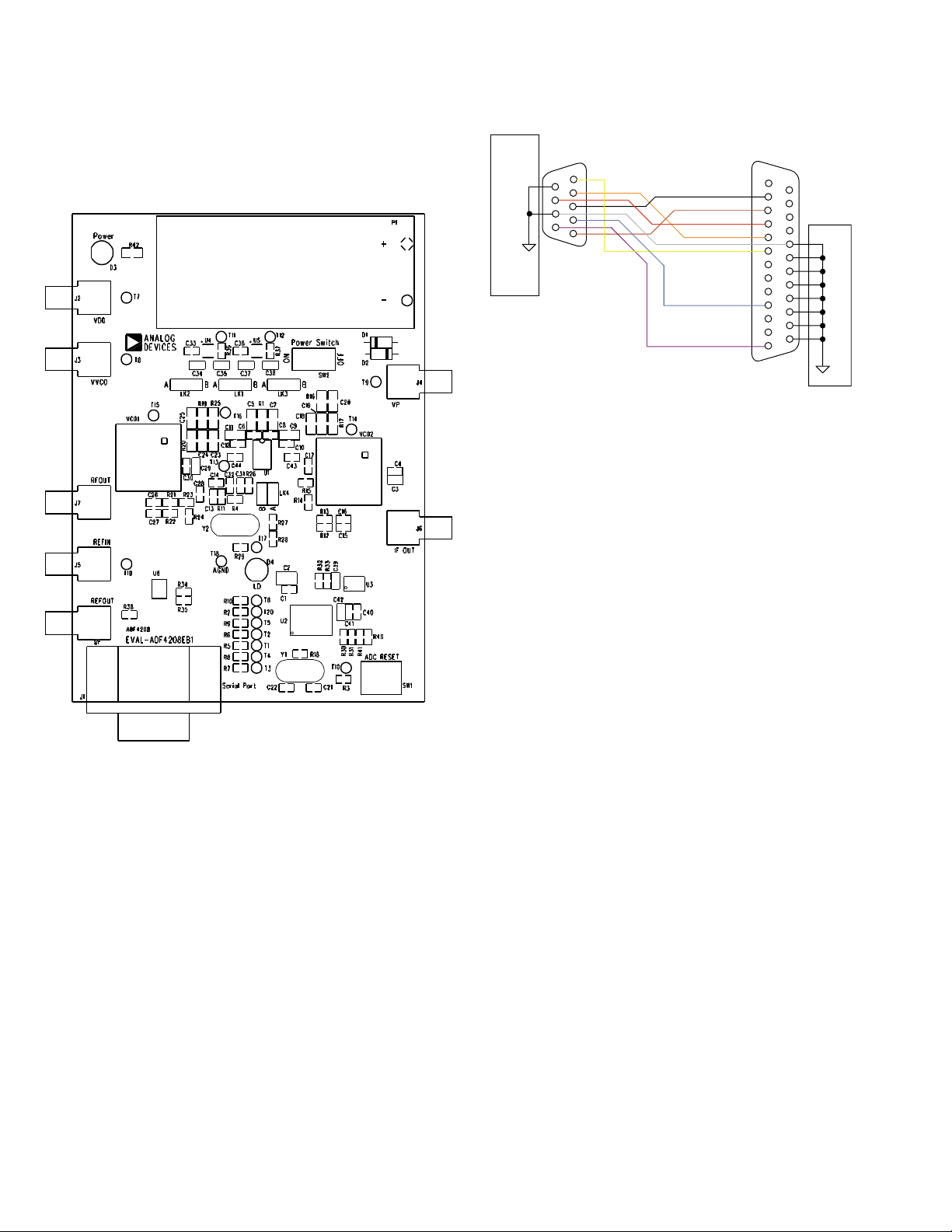
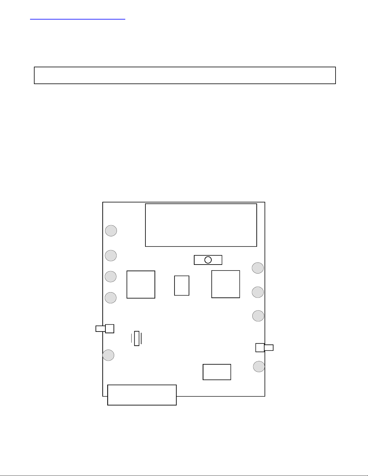
Hardware Description
The evaluation board comes with a cable for connecting to
the printer port of a PC. The silk screen and cable diagram for
the evaluation board are shown below. The board
schematic is shown on pages 3 and 4.
EV AL-ADF4208EB1
EVAL-ADF411X
EVAL-ADF421X
1
6
2
7
3
8
4
9
5
9 Way
Female D-Type
To
ADF411X
ADF421X
Evaluation
Board
Brown - DATA
Figure 2. PC Cable Diagram
connectors. If the user wishes they may use their own
power supplies and use the reference output. In this case,
they need to insert SMA connectors to as shown on the
silkscreen and block diagram.
The AD7706 A/D converter is used to monitor the power
supply voltage and current consumption of the ADF4208.
This helps the user pick the optimum synthesizer settings for
power consumption and also provides an alert if the battery
voltage is too low to sustain the required 3V or 5V for the
board supply.
Black - CLK
Red - LE
Orange - CE
White - GND
Yellow
Purple
1
2
3
4
5
6
7
8
9
10
Blue
11
12
13
25 Way Male
D-Type
To
PC Printer Port
14
15
16
17
18
19
20
21
22
23
24
25
PC
Figure 1. Evaluation Board Silkscreen
The board is powered from a single 9V battery. The
power supply ciruitry allows the user to choose either 3V
or 5V for the ADF4208 V
supply. The default settings are 3V for the ADF4208 V
and VP, and for the VCO
DD
DD
and 5V for the ADF4208 VP and for the VCO supply. It
is very important to note that the ADF4208 V
never exceed the ADF4208 V
. This can damage the de-
P
should
DD
vice.
All components necessary for LO generation are catered
for on-board. The crystal oscillator circuit provides the
necessary 10MHz reference frequency. The addition of an
SMA connector allows an external reference to be used
(Please consult circuit diagram to see what components
are needed to be added or removed for this). The PLL
requires a loop filter and VCO for both the IF and RF
sides to complete the dual PLL. The output is available
at RF OUT and IF OUT through standard SMA
–2–
REV.PrA 02/00

EVAL-ADF4208EB1
Figure 3. Evaluation Board Circuit Diagram (Page 1)
–3–
REV.PrA 02/00

EV AL-ADF4208EB1
Figure 4. Evaluation Board Circuit Diagram (Page 2)
–4–
REV.PrA 02/00

Software Description
The software comes on a CD. If the user runs
“ADF4XXXEvaluationSoftware.exe” on the CD, then the
install wizard installs the software. Follow the on-screen
directions. The software will be installed in a default
directory called “C:\Program Files\Analog
Devices\ADF4xxx Evaluation Software”. To run the
software, simply double click on "ADF4XXX Eval
Software.exe".
The front panel of the evaluation board software is shown
below.
When the device window appears, choose the ADF4208
and click OK. The main software screen now appears.
Follow the steps below for initial setup to interface to the
part.
Click on Choose Port, and the Port Connector window
will appear. Choose the port that the cable is connected to
on the PC and click OK. (Normally LPT1)
EVAL-ADF4208EB1
Click on REF IN Frequency, and the REF IN Frequency
window will appear. Enter the reference frequency being
used and click OK. This will be 10MHz with the Crystal.
Click on RF VCO Output Frequency, and the Output
Frequency window will appear. Enter the output frequency
and PFD reference frequency, and click OK. Repeat this
for the IF side.
Click On Prescaler, and the Prescaler window will appear.
Grab the pointer, and choose the desired prescaler value.
Click OK.
Click on the RF PD Polarity button to set the RF PD Polarity
bit High.
Click on Charge Pump Current Setting 2 or Charge Pump
Current Setting 1 and the Current Setting window will appear. Grab the pointer to set the Charge Pump Current Setting. Click OK.
The data is now set up, and other features can now be examined by the user.
Figure 5. Software Front Panel
–5–
REV.PrA 02/00

EV AL-ADF4208EB1
Table 1. Bill of Materials for the EVAL-ADF4208EB1
Qty Refere nce Description Ma nufa cturer PCB DECAL VALUE
1 U1 ADF 4208BRU ADI TSS O P -20 ADF 4208BRU
1 U2 AD770 6B R ADI SO16WB AD770 6B R
1 U3 AD780AR ADI SO8NB AD780AR
1 U4 ADP3300A RT-5 ADI SOT23-6 ADP3300A RT-5
1 U5 ADP3300A RT-3 ADI SOT23-6 ADP3300A RT-3
1 U6 Do Not Insert Fairchild SO T23-5 NC7S M 508
1 V C O 1 Do N o t Ins e rt V a ri -L
1 V C O 2 Do N o t Ins e rt V a ri -L
1 Y1 4.9152MHz Crystal
1 Y2 10M Hz Crys tal
1 D1 SD103 C S c hott ky D iode General Se m ico nduc tor DO35 SD103 C
1 D2 IN4001 D035 FE C 365-117
1 D3 Red Low P ower LE D Vis hay LED FE C 657-130
1 D4 Green Low P ower LE D (Do Not Ins ert) V is hay LED FEC 65 7-141
6 C1 C5 C7 C9 C11 C41 Multi Layer Ceramic Capacitor M urata Case 0603 0.1uF
1 C2 Tantalum Capac itor AV X CAP \ TAJ_B 10uF 6.3V
2 C3 C29 Tantalum Capac itor AV X CAP \ TAJ_A 22uF 6.3V
6 C4 C6 C8 C10 C 12 C30 Multi Lay er Ceramic Cap acit or M u rata Cas e 0 603 10 pF
2 C1 3 -14 D o No t Ins e rt Mura t a Cas e 06 0 3 1n F
8 C15-17 C26-28 C43-44 Multi Layer Ceram ic Capac itor Murata Cas e 0603 100pF
1 C18 Do Not Insert Murata Case 0805
1 C19 Do Not Insert Murata Case 0805
1 C20 Do Not Insert Murata Case 0805
4 C21-22 C31-32 Multi Layer Ceramic Capacitor M urata Case 0603 33pF
1 C23 Do Not Insert Murata Case 0805
1 C24 Do Not Insert Murata Case 0805
1 C25 Do Not Insert Murata Case 0805
3 C33 C36 C40 Multi Layer Ceramic Capacitor M urata Case 0603 10nF
2 C34 C37 Tantalum Capac itor AV X CAP \ TAJ_A 1uF 16V
2 C35 C38 Tantalum Capac itor AV X CAP \ TAJ_A 4.7uF 10V
2 C39 C42 Tantalum Capac itor AV X CAP \ TAJ_A 10uF 6.3V
Vectron International
Vectron International
HC49 low profile VXA4-1011
HC49 low profile VXA4-1B2-10M 00
1 R1 Resis tor (S urface Mount ) Bourns Cas e 0 805 20r 1.0%
7 R2 R5-10 Resis tor (S urface Mount ) Bourns Cas e 0 603 330r 1.0%
1 R3 Resis tor (S urface Mount ) Bourns Cas e 0 603 3k 3 1. 0%
2 R4 R18 Resis tor (S urface Mount ) Bourns Cas e 0 603 1M 1. 0%
1 R11 Do Not Insert Bo urns Cas e 0603 51 r 1.0%
6 R12-14 R21-23 Resis tor (S urface Mount ) Bourns Cas e 0 603 18r 1.0%
2 R15 R24 Resis tor (S urface Mount ) Bourns Cas e 0 603 51r 1.0%
1 R16 Do Not Insert Case 0805
1 R17 Do Not Insert Case 0805
1 R19 Do Not Insert Case 0805
1 R20 Do Not Insert Case 0805
1 R25 Do Not Insert Case 0805
1 R26 Res isto r (Surface M ount) Bo urns Cas e 0603 1k 1.0%
3 R27-29 Resist or (Surface M ount) Bo urns Cas e 0603 10k 1. 0%
6 R30-33 R40-41 Resis tor (S urface Mount ) Meggit t Ca s e 0603 100k 0. 1%
3 R34-35 R38 Do Not Insert Case 0603 0r 1.0%
2 R36 R37 Resis tor (S urface Mount ) Bourns Cas e 0 603 330k 1 .0%
1 R42 Res isto r (Surface M ount) Bo urns Cas e 0603 4k7 1.0%
1 SW1 Pus h B ut ton S wit ch Om ron SW\P B -S M A LL FE C 176-986
1 SW2 SP DT S witc h - (W as hable) Apem SW_S IP-3P FEC 150-559
20 T1-20 Red Testpoint W Hug hes TESTP OINT FE C-240-345
1 J1 9 PIN D-TYPE MALE (HORIZ) McM urdo DCON9M F E C 150-750
5 J2 J3 J4 J5 J8 Do N ot Insert SMA
2 J6 J7 GO LD 50Ω SMA SOCKET Pasternack SMA PE 4118
3 LK1 LK 2 LK3 3 pin header Harwin S IP-3P FE C 512-047
1 LK4 4 pin h eader (2x2) Harwin FE C 512-035
4 LK1-4 Sh orting Sh unt Harwin FE C 150-410
4 Eac h Corner Rubber Stic k -On Fe et 3M FE C 148-922
2 P1 P air PC B s nap-on battery c onnec tor Key s tone BATT_PP 3 FEC 723-988
1 P1 9V P P 3 B at tery Duracell FE C 908-526
1 PCB EV AL-ADF 4208E B1
–6–
REV.PrA 02/00
 Loading...