

PRELIMINARY TECHNICAL DATA
现货库存、技术资料、百科信息、热点资讯,精彩尽在鼎好!
Evaluation Board Documentation
=
Preliminary Technical Data
FEATURES
Evaluation Board is designed to be used together with
accompanying software to implement a fully functional
Energy Meter (Watt-Hour Meter).
Easy connection of various external transducers via
screw terminals.
Easy modification of signal conditioning components
using PCB sockets.
LED indicators on logic outputs CF, ZX, SAG and IRQ.
Optically isolated data output connection to PC parallel port.
Optically isolated frequency output (CF) to BNC.
External Reference option available for
on-chip reference evaluation.
GENERAL DESCRIPTIONGENERAL DESCRIPTION
GENERAL DESCRIPTION
GENERAL DESCRIPTIONGENERAL DESCRIPTION
The ADE7756 is a high accuracy electrical power measurement IC with a serial interface and a pulse output.
The ADE7756 incorporates two second order sigma delta
ADCs, reference circuitry, temperature sensor and all the
signal processing required to perform active power and
energy measurement.
This documentation describes the ADE7756 evaluation kit
Hardware and Software functionality. The ADE7756
AD7756 Energy metering IC
EVAL-ADE7756EB
evaluation board, together with the ADE7756 data sheet
and this documentation provides a complete evaluation
platform for the ADE7756.
The evaluation board has been designed so that the
ADE7756 can be evaluated in the end application, i.e.,
Watt-Hour Meter. Using the appropriate transducers on
the current channel (e.g., shunt, CT etc.) the evaluation
board can be connected to a test bench or high voltage
(240V rms) test circuit. An on-board resistor divider
network provides the attenuation for the line voltage. This
application note also describes how the current transducers
should be connected for the best performance.
The evaluation board (watt-hour meter) is configured and
calibrated via the parallel port of a PC. The data interface
between the evaluation board and the PC is fully isolated.
Windows
board which allows it to be quickly configured as an
energy meter.
The evaluation board also functions as a stand alone
evaluation system which can be easily incorporated into an
existing system via a 25 way D-Sub connector.
The evaluation board requires two external 5V power
supplies (one is required for isolation purposes) and the
appropriate current transducer.
TM
based software is provided with the evaluation
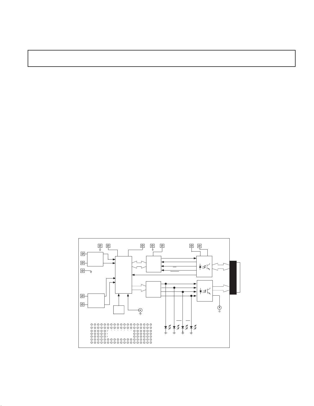
FUNCTIONAL BLOCK DIAGRAM
V1P
V1N
AGND
V2N
V2P
AGND
Filter
Network
Filter
Network
&
Attenuation
Optional External
2.5V Reference
AV
DD
ADE7756
AD780
PROTOTYPE
AREA
DV
DD
BNC
External
Clock in
DGND
74HC08
74HC08
REV. PrB 01/01
Information furnished by Analog Devices is believed to be accurate and
reliable. However, no responsibility is assumed by Analog Devices for its
use, nor for any infringements of patents or other rights of third parties
which may result from its use. No license is granted by implication or
otherwise under any patent or patent rights of Analog Devices.
+5V
DOUT
SCLK
DIN
CS
RESET
CF ZX
SAG
One Technology Way, P.O. Box 9106, Norwood. MA 02062-9106, U.S.A.
Tel: 617/329-4700 Fax: 617/326-8703
V+
Isolated Frequency
IRQ
V-
Connector to
PC Parallel
Port
BNC
CF
output
EVAL-ADE7756EB
PRELIMINARY TECHNICAL DATA
PRELIMINARY TECHNICAL DATA
ANALOG INPUTS (SK1 AND SK2)ANALOG INPUTS (SK1 AND SK2)
ANALOG INPUTS (SK1 AND SK2)
ANALOG INPUTS (SK1 AND SK2)ANALOG INPUTS (SK1 AND SK2)
Voltage and current signals are connected at the screw terminals SK1 and SK2 respectively. All analog input signals are
filtered using the on-board anti-alias filters before being
presented to the analog inputs of the ADE7756. The
default component values which are shipped with the
evaluation board are the recommended values to be used
with the ADE7756. The user can easily change these
components, however this is not recommended unless the
user is familiar with sigma-delta converters and also the
criteria used for selecting the component values for the
analog input filters—see AN-559 for a more comprehensive description of the anti-alias filters and their function.
Current sense inputs (SK2)
SK2 is a three-way connection block which allows the
ADE7756 to be connected to a current transducer. Figure
1 shows the connector SK2 and the filtering network
which is provided on the evaluation board.
The resistors SH1A and SH1B are by default not populated. They are intended to be used as burden resistors
when a CT is used as the current transducer—see using a
CT as a the current transducer.
The RC networks R41/C11 and R42/C21 are used to
provide phase compensation when a shunt is being used as
the current transducer—see using a shunt as the current
transducer. These RC networks are easily disabled by
placing JP15 & JP25 and removing C11 & C21 (socketed).
The RC networks R50/C50 & R51/C51 are the anti-alias
filters which are required by the on-chip ADCs. The
default corner frequency for these LPFs (Low Pass
Filters) is selected as 4.8kHz (1kΩ & 33nF). These filters
can easily be adjusted by replacing the components on the
evaluation board. However before adjusting the component values of R50, R51, C50 or C51 the user should first
review application note AN-559.
ADE7756
JP2
JP15
R41
100Ω
JP25
R42
100Ω
JP4
SH1A
SK2 1
SK2 2
SH1B
SK2 3
Figure 1 — Current Channel on the ADE7756 evaluation
C11
33nF
C21
33nF
board
JP1
R50
1kΩ
JP3
R51
1kΩ
TP1
C50
33nF
C51
33nF
V1P
TP2
V1N
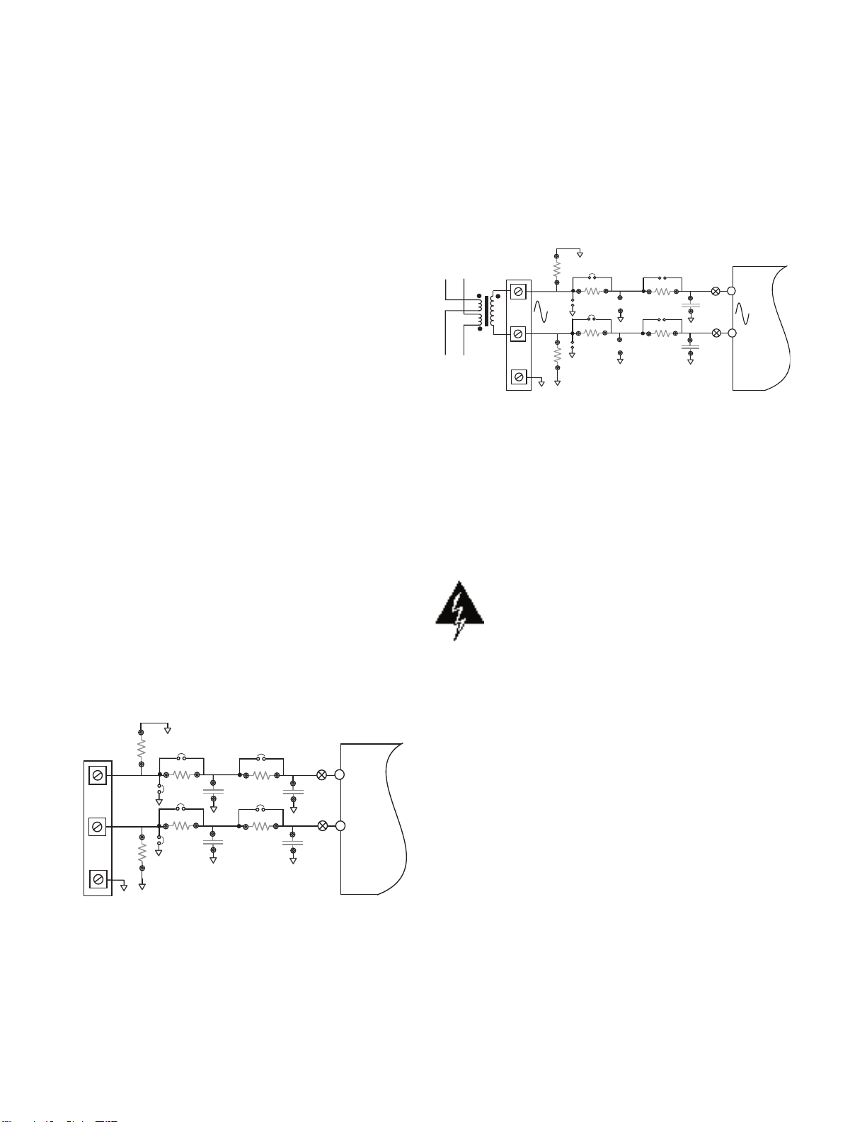
Using a CT as the current transducer
Figure 2 shows how a CT can be used as a current
transducer in a signal phase 3-wire distribution system.
This is how electrical energy is distributed to residential
users in the United States. Phase A and Phase B are
nominally 180° out of phase. The vector addition of the
two currents is easily achieved by using two primary turns
of opposite polarity on the CT.
33nF
33nF
TP1
TP2
ADE7756
V1P
355mV
rms
V1N
Phase A
I max = 80A
CT
1:1800
Phase B
SH1A
SH1B
JP15
4Ω
100Ω
JP2
JP25
100Ω
JP4
4Ω
JP1
1kΩ
JP3
1kΩ
Full Scale
differential input = 1V
Gain = 2
Figure 2 — CT connection to Current Channel
The CT secondary current is converted to a voltage by
using a burden resistance across the secondary winding
outputs. Care should be taken when using a CT as the
current transducer. If the secondary is left open, i.e., no
burden is connected, a large voltage could be present at
the secondary outputs. This can cause an electrical shock
hazard and potentially damage electronic components.
Warning!
Using a CT without a burden resistor
can lead to electrical shock.
When using a CT as the current sensor, the phase compensation network for a shunt application should be
disabled. This is achieved by closing jumpers JP15/JP25
and removing C11/C21.
The anti-alias filters should be enabled by opening
jumpers JP1/JP3—see Figure 2.
Most CTs will have an associated phase shift of between
0.1° and 1° at 50Hz/60Hz. This phase shift or phase error
can lead to significant energy measurement errors, especially at low power factors—see AN-559 for more information. However this phase error can be corrected by
writing to the Phase Calibration register (PHCAL) in the
ADE7756. The software supplied with the ADE7756
evaluation board allows user adjustment of the Phase
Calibration register. See the Evaluation Software Description
for more information.
For this example, notice that the maximum analog input
range on Channel 1 is set to 1V. And the Gain for Channel 1 has be set to 2. The maximum analog input range
and gain are set via the Gain register (GAIN)—see the
ADE7756 data sheet. The evaluation software allows the
user to configure the channel range and gain. This means
that the maximum peak differential signal on Channel 1 is
0.5V.
–2–
REV. PrB 01/01
PRELIMINARY TECHNICAL DATA
PRELIMINARY TECHNICAL DATA
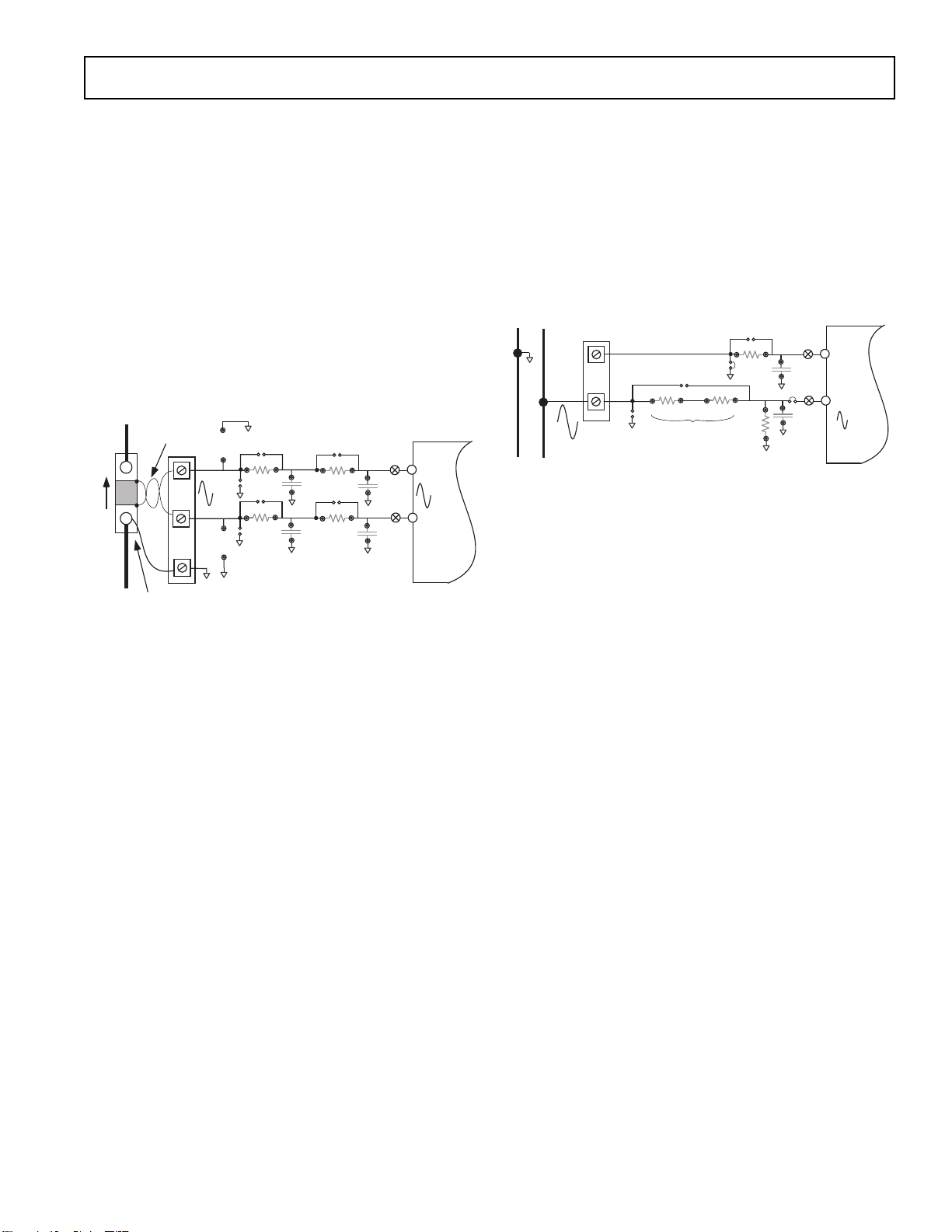
Using a shunt resistor as the current transducer
Figure 3 shows how a shunt resistance can be used to
perform the current to voltage conversion required for the
ADE7756. A shunt is a very cost effective way to perform
the current to voltage conversion in a two-wire, singlephase application. No isolation is required in a two-wire
application and the shunt has advantages over the CT
arrangement. For example a shunt does not suffer from dc
saturation problems and the phase response of the shunt is
linear over a very wide dynamic range. Although the shunt
is predominately resistive, it does have parasitic reactive
elements (inductance) which can become significant, even
at 50Hz/60Hz. This means that there can be a small phase
shift associated with the shunt. However once it is understood the phase shift is easily compensated with the filter
network R41/C11 and R42/C21—see AN-559 for a
detailed discussion of this issue.
Twisted pair
connection
200µΩ
80A
BVM-D-R0002-5.0
JP2
JP15
100Ω
JP25
100Ω
JP4
JP1
1kΩ
33nF
JP3
1kΩ
33nF
Full Scale
differential input = 0.5V
Gain = 16
Figure 3 — Shunt connection to Current Channel
The shunt used in this example is a 200µΩ manganin type.
The resistance of the shunt should be as low as possible in
order to avoid excessive power dissipation in the shunt.
Although the shunt is fabricated from a special alloy
(manganin) which has a very low temperature coefficient
of resistance, excessive heating due to power dissipation
can cause measurement inaccuracies when operating at
heavy loads over extended periods of time.
The manganin shunt used in this example (BVM-DR0002-5.0) is designed specifically for energy metering
applications and is supplied by Isotek Corp.
(http://www.isotekcorp.com).
This shunt is PCB mountable with a current carrying
ability of 70A rms. The technical data supplied by Isotek
Corp. gives detailed information regarding PCB layout.
Figure 3 shows how the shunt can be connected to the
evaluation board. Two sense wired should be soldered to
the shunt at the copper/manganium junctions as shown.
These sense wires should be formed into a twisted pair to
reduce the loop area which will reduce antenna effects. A
connection for the common mode voltage can be made at
the connection point for the current carrying conductor—
see Figure 3.
TP1
33nF
TP2
33nF
ADE7756
V1P
16mV
rms
V1N
EVAL-ADE7756EB
Voltage sense inputs
The voltage input connections on the ADE7756 evaluation board can be directly connected to the line voltage
source. The line voltage is attenuated using a simple
resistor divider network before it is presented to the
ADE7756. Because of the relatively large signal on this
channel and the small dynamic range requirement, the
voltage channel can be configured in a single-ended
configuration. Figure 4 shows a typical connection for the
line voltage.
C54
33nF
JP51
C53
33nF
ADE7756
TP5
V2N
TP4
V2P
200 - 300 mV
rms
JP9
JP10
255kΩ
R54
R57
1kΩ
JP3
R56
1kΩ
Neutral
Phase
SK1 1
SK1 2
100 - 250 V rms
JP8
R53
255kΩ
Attenuation
JP7
Network
Figure 4 — Voltage Channel on the ADE7756 evaluation
board
Note that the analog inputs V2N is connected to AGND
via the anti-alias filter R57/C54 using JP10. Jumper JP9
should be left open.
The voltage attenuation network is made up of R53, R54
and R56. The maximum signal level permissible at V2P is
1V peak. Although the ADE7756 analog inputs can
withstand ±6V without risk of permanent damage, the
signal range should not exceed ±1V with respect to
AGND, for specified operation.
The attenuation network can be easily modified by the
user to accommodate any input signal levels. However the
value of R56 (1kΩ) should not be altered as the phase
response of Channel 2 should match that of Channel 1—
see AN-559 (Attenuation Network).
REV. PrB 01/01
–3–
PRELIMINARY TECHNICAL DATA
EVAL-ADE7756EB
JUMPER SETTINGS
JUMEPER OPTION DESCRIPTION
JP1 Closed This will short out R50. The effect is to disable the anti-alias filter on the
analog input V1P. Default Open.
Open Enable the anti-alias filter on V1P.
JP2 Closed This will connect the analog input V1P to ground. Default Open.
JP3 Closed This will short out R51. The effect is to disable the anti-alias filter on the
analog input V1N. Default Open.
Open Enabe the anti-alias filter on V1N.
JP4 Closed This will connect the analog input V1N to ground. Default Open.
JP5 A This connects the buffered logic output
IRQ to the LED1.
B This connects the buffered logic output
via an optical isolator.
JP6 A This connects the buffered logic output
B This connects the buffered logic output
via an optical isolator.
JP7 Closed This will short the attenuation network on Channel 2. Default open.
JP8 Closed This will connect the analog input V2P to ground. Default Open.
JP9 Closed This will short out R57. The effect is to disable the anti-alias filter on the
analog input V2N. Default Open.
Open Enable the anti-alias filter on V2N.
JP10 Closed This will connect the analog input V2N to ground. Default Open.
JP11 Closed This will connect the Analog and Digital ground planes of the PCB. Default
Closed.
JP12 A This connects the buffered logic output CF to the LED4.
B This connects the buffered logic output CF to BNC2 connector via an optical
isolator.
JP13 Closed This will connect an external reference 2.5V (AD780) to the ADE7756.
Open This will enable the ADE7756 on-chip reference.
JP14 Closed This will connect the optical isolator ground to the evaluation board gound
(DGND). If full isolation between the evaluation board and PC is required,
this jumper should be left open.
IRQ to pin 10 on the D-Sub connector
SAG to the LED2.
SAG to pin 11 on the D-Sub connector
JP15 Closed This will short out R41. The effect is to disable the phase compensation filter
(for shunts) on the analog input V1P. Default Closed.
JP19 A This connects the buffered logic output ZX to the LED3.
B This connects the buffered logic output ZX to pin 12 on the D-Sub connector
via an optical isolator.
JP20 Closed This connects the AVDD and DVDD supply for the evaluation board together.
Default Closed.
JP21 Closed This connects the DVDD and +5V (buffers) supply for the evaluation board
together. Default Closed.
JP25 Closed This will short out R42. The effect is to disable the phase compensation filter
(for shunts) on the analog input V1N. Default Closed.
JP51 Closed This will short out disconnect Analog input V2P from the ADE7756. Default
Closed.
–4–
REV. PrB 01/01
PRELIMINARY TECHNICAL DATA
PRELIMINARY TECHNICAL DATA
JP20
JP1
JP15
JP2
JP4
JP10
JP7
JP8
JP25
JP9
JP51
JP3
Figure 5 - ADE7756 evaluation board jumper positions
SETTING UP THE ADE7756 EVALUATION BOARDSETTING UP THE ADE7756 EVALUATION BOARD
SETTING UP THE ADE7756 EVALUATION BOARD
SETTING UP THE ADE7756 EVALUATION BOARDSETTING UP THE ADE7756 EVALUATION BOARD
Shown below is a typical set up for the ADE7756 evaluation board. In this example a kWh meter for a 3 wire,
single phase distribution system is shown. For a more
detailed description on how to use a CT as a current
transducer see the Current Sense Inputs section of this documentation. The line voltage is connected directly to the
evaluation board as shown. Note JP7 should be left open
to ensure that the attenuation network is not bypassed.
Also note the use of two power supplies. The second
power supply is used to power the optical isolation. With
JP14 left open, this will ensure that there is no electrical
connection between the high voltage test circuit and the
PC. The power supplies should have floating voltage
outputs.
JP13
AD7756
JP11
EVAL-ADE7756EB
JP21
AB
JP5
JP6
JP19
JP12
AB
The evaluation board is connected to the PC parallel port
using the cable supplied. The cable length should not
exceed 6 feets (2 meters) or the serial communication
between the PC and the evaluation board may become
unpredictable and error prone.
When the evaluation board has been powered up and is
connected to the PC, the supplied software can be
launched. The software will automatically start in energy
meter mode. The next section describes the ADE7756
evaluation software in detail and how it can be installed
and uninstalled.
JP14
REV. PrB 01/01
Neutral
110V
Load
110V
5.000 V
-
+
JP13 = Open
JP14 = Open
JP15 = Closed
JP19 = B
JP20 = Closed
JP21 = Closed
JP25 = Closed
1.0666 Hz
Phase B
110V
10A
10A
Load
Phase A
1:2000
CT
AGND
220V
5.000 V
SK2
SK1
2.5Ω
SH1A
SH1B
2.5Ω
-
+
25mV
R53
255kΩ 255kΩ
JP8
V1P
V1N
25mV
JP7
JP10
DVDD
JP1 = Open
JP2 = Open
JP3 = Open
JP4 = Open
JP5 = B
JP6 = B
JP9
R57
1kΩ
R54
C53
33nF
DGND
SK4
C54
33nF
450mV
+5V
1kΩ
JP7 = Open
JP8 = Open
JP9 = Open
JP10 = Closed
JP11 = Closed
JP12 = B
V2N
V2P
Figure 6 - Typical set up for the ADE7756 evaluation board
–5–
V+ V-
SK5
BNC2
To PC
Parallel Port

PRELIMINARY TECHNICAL DATA
EVAL-ADE7756EB
ADE7756 EVALUATION SOFTWAREADE7756 EVALUATION SOFTWARE
ADE7756 EVALUATION SOFTWARE
ADE7756 EVALUATION SOFTWAREADE7756 EVALUATION SOFTWARE
The AD7756 evaluation board is supported by Windows
based software which will allow the user to access all the
functionality of the ADE7756. The software is designed to
communicate with the ADE7756 evaluation board via the
parallel port of the PC.
Installing the AD7756 Software
The ADE7756 Software is supplied on three 3.5'' 1.44MB
floppy disks. The minimum requirements for the PC are
Pentium II 233MHz, 32 MB RAM, 10MB free HD space
and at least one PS/2 or ECP parallel port . To install the
software place disk #1 in the floppy drive and double click
"setup.exe". This will launch the set up program which
will automatically install all the software components
including the uninstall program and create the required
directories. When the set up program has finished installing the "ADE7756Eval" program the user will be
prompted to install the National Instruments run-time
engine. This software was developed using National
Instruments LabView software and the run-time engine is
required in order to run the "ADE7756Eval" program.
When prompted simply place disk #2 in the floppy drive
and hit return. Follow the on-screen instructions to
complete the installation. You will need to reboot your
computer to complete the installation.
To launch the software simply go to the
Start—>Programs—>ADE7756 menu and click on
"ADE7756Eval".
Metering Mode
When the software is launched, the program automatically
starts in Meter Mode. In this mode the evaluation board
can be used as a fully functional energy meter. When the
appropriate line voltage, test current, frequency, and meter
constant have been set up, the user can use the calibration
routine to remove any error associated with the transducers. The CF output can be used with a standard frequency
counter to check the accuracy. The measured CF output
frequency should be adjusted to match the theoretical CF
freq. of the Eval software.
Note that the calibration routine does not automatically
remove phase errors associated with a CT or other
transducer. These must be removed first by using the
ADE7756 PHCAL Register. This is explained later.
Instantaneous Power, Voltage, and Current RMS calculations are also available in this window. They are processed
using the Waveform Sampling routine with the number of
samples defined in this mode.
Uninstalling the ADE7756 Evaluation Software
Both the "ADE7756Eval" program and the NI run-time
engine are easily uninstalled by using the Add/Remove
Programs facility in the control panel. Simply select the
program to uninstall and click the Add/Remove button.
Figure 8 - Meter Mode
Note also that the input signal range and gain must be set
for the PGAs on the Channel 1 and Channel 2. This will
ensure that the output signal range from the transducers is
matched to the analog inputs. For example, in the meter
example shown in Figure 6 the line voltage is attenuated
to approximately 215mV rms or 300mV peak. By selecting a gain of 2 for the PGA in Channel 2, the peak
differential input signal is set to 500mV. Similarly for
Channel 1, assuming a maximum current of 120A the
maximum differential output signal from the CT is
300mV. Therefore the full-scale differential input signal
level is set to 500mV by setting the gain to 2—see Table I
in the ADE7756 data sheet. The PGA settings are made
through the main selection menu. To get to the main
selection menu click the "Quit to Menu" button at any
time.
Figure 7 — Uninstalling the ADE7756 Eval Software
–6–
REV. PrB 01/01

PRELIMINARY TECHNICAL DATA
PRELIMINARY TECHNICAL DATA
Calibrating the meter
In order to calibrate the energy meter, the line voltage,
test current, line frequency and meter constant are entered
as shown in Figure 8. In this example the line voltage is
entered as 220V, test current is 5A, frequency is 50Hz and
the required meter constant is 3200imp/kWh. With the
parameters entered and the voltage and current circuits
energized, click the calibrate button. The software will
then execute the calibration routine and automatically start
to register energy.
If a HP/AGILENT53131A frequency counter is connected
to a GPIB card of the desktop computer, the software will
automatically read the value of the CF frequency and
process the calibration routine. In this case, the calibration
takes about 5 seconds and the user will be notified when it
is complete.
Otherwise, calibration can be proceeded by changing
CFDIV and APGAIN registers as explained in the
ADE7756 datasheet. The measured CF output frequency
is then adjusted to match the theoretical CF freq. of the
Eval software.
Ensure that the analog input signal levels have been
matched to the transducer output signal levels as described
previously.
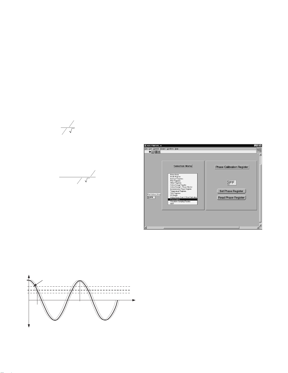
Main Selection
In order to access all the internal registers of the
ADE7756 the user must return to the Main Selection
Menu. Figure 9 shows the Main Selection Menu and the
various options. From here such things as phase compensation and Channel 1 and Channel 2 PGA setting can be
made.
EVAL-ADE7756EB
To select another option from the menu simply click
on the selection menu. By using the selection menu
the user can read and write the registers of the
ADE7756. This software should be used in conjunction with the ADE7756 data sheet.
Waveform Sampling Routine
In this mode, the Evaluation Software programs the
ADE7756 for Waveform sampling with an updated
rate of 3.5ksps (CLKIN/1024). The user can define
the number of samples needed and select the Signal
Waveform to transfer. Three parameters are processed
when the waveform is displayed: RMS value, Mean
value and Standard Deviation.
When using this feature with sinewave signals, the
user should be aware that if the samples represent a
non entire number of period of the selected signal
then the RMS and Mean values are biased. To correct
this, the number of samples should be chosen to give
an entire number of signal cycles:
×
#
samples
Note: If Channel 1 and Channel 2 are at the same
frequency then the signal frequency of the Multiplier
Waveform shoud be chosen as twice the Channel1
Frequency to correct the Signal Processing bias.
On line help
The ADE7756 evaluation software also comes with
on-line help features. In order to activate the help
function goto Help on the Menu Bar and select "Show
Help"—see Figure 10. A Help Window will open. In
order to get a description of a particular option (e.g.,
button, text box etc.) move the cursor over the item of
interest. The Help window will display a description
of the selected item.
=
1024
7756#
×
FrequencySignal
FrequencyCLKINADEcyclessignal
Figure 9—Selection Menu & PGA Settings
REV. PrB 01/01
Figure 10—On-line Help Function.
–7–
EVAL-ADE7756EB
PRELIMINARY TECHNICAL DATA
Measuring CT Phase Errors using the ADE7756
The ADE7756 itself can be used to measure a CT (and
external components) phase error during calibration. The
assumption is that the ADE7756 has no internal phase
error (PHCAL = 00 hex) and the error due to external
components is small (<0.5°). The procedure is based on a
two point measurement, at PF=1 and PF = 0.5 (lag). The
PF is set up using the test bench source and this source
must be very accurate. The ADE7756 should be configured for energy measurement mode.
An energy measurement is first made with PF=1 (measurement A). A second energy measurement should be
made at PF=0.5 (measurement B). The frequency output
CF can be used for this measurement. Using the formula
shown below the phase error is easily calculated:
A
B
−
1
−
ErrorPhase
tan)(
=°
2
A
3
⋅
2
For example, using the frequency output CF to measure
power, a frequency of 3.66621Hz is recorded for a PF=1.
The PF is then set to 0.5 lag and a measurement of
1.83817Hz is obtained. Using the formula above the
phase error on Channel 1 is calculated as:
Using the Phase Calibration to correct
small (<0.5°) external phase errors
From the previous example it is seen that the CT introduced a phase lead in Channel 1 of 0.091° . Therefore
instead of 60° phase difference between Channel 1 and
Channel 2, it is actually 59.89°. In order to bring the
phase difference back to 60°, the phase compensation
circuit in Channel 2 is used to introduce an extra lead of
0.091°. This is achieved by reducing the amount of time
delay in Channel 2.
The maximum time delay adjustment in Channel 2 is
±143µs with a CLKIN of 3.579545MHz. The PHCAL
register is a signed 2's complement 6 bit register. Therefore each LSB is equivalent to 4.47µs. In this example the
line frequency is 50Hz. This means each LSB is equivalent to (360° x 4.47µs x 50) = 0.08°. To introduce a lead
of 0.091° the delay in Channel 2 must be reduced. This is
achieved by writing -1 (FFh) or +0.08° to the PHCAL
register.
−
=°
ErrorPhase
tan)(
66621.3
2
⋅
3
2
°+=
091.0
66621.3
−
83817.1
1
The formula will also give the correct sign for the phase
error. In this example the phase error is calculated as
+0.091° at the input to the Channel 1 of ADE7756. This
means that the CT has introduced a phase lead of 0.091°.
Therefore the phase difference at thr input to Channel 1 is
now 59.89° lag instead of 60° lag. Determining whether
the error is a lead or lag can also be figured intuitively
from the frequency output. Figure 11 shows how the
output frequency varies with phase (cos{φ}). Since the
output frequency B (1.83817Hz) at the PF=0.5 lag setting
in the example is actually greater than A/2 (1.833105Hz),
this means the phase error between Channel 1 and Channel 2 was actually less than 60°. This means there was
additional lead in Channel 1 due to the CT.
CF (Hz)
PF=1
PF>0.5
PF=0.5
PF<0.5
PF=0
Frequency B > A/2
Phase difference < 60
60
lag
360
Phase lag
Figure 10—CF Frequency Vs Phase(PF)
Figure 11—Writing to the PHCAL register to correct
phase error
Correcting large external phase errors
In this example the phase correction range at 50Hz is only
approximatey ±2.5°. However it is best to only use the
PHCAL register for small phase corrections, i.e., <0.5°.
If larger corrections are required the larger part of the
correction can be made using external passive component.
For example the resistors in the anti-alias filter can be
modified to shift the corner frequency of the filter so as to
introduce more or less lag. The lag through the anti-alias
filters with 1kΩ and 33nF is 0.56° at 50Hz. Fine adjust
can be made with the PHCAL register. Note that typically
CT phase shift will not vary significantly from part to
part. If a CT phase shift is 1°, then the part to part
variation should only be about ±0.1°. Therefore the bulk
of the phase shift (1°) can be canceled with fixed component values at design. The remaining small adjustments
can be made in production using the PHCAL register.
–8–
REV. PrB 01/01

PRELIMINARY TECHNICAL DATA
PRELIMINARY TECHNICAL DATA
EVAL-ADE7756EB
Evaluation board BOM
Designator Value Description
R3, R5, R6, R13, R22,
R30, R31, R33, R34, R37 100Ω, 5%, ¼W Resistor, no special requirements
R2, R7, R8, R9, R10,
R39, R40 10kΩ, 5%, ¼W Resistor, no special requirements
R1, R14 - R27, R36 820Ω, 5%, ¼W Resistor, no special requirements
R50, R51, R52, R57 1kΩ, 0.1%, ¼W ±15 ppm/°C Resistor, good tolerance, used as part of the analog filter
network.These resistors are not soldered, but are plugged into PCB
pin sockets for easy modification by the customer. Low drift
WELWYN RC55 Series, FARNELL part no. 339-179
R53, R54 255kΩ, 0.1%, ¼W Pin socketed, ±15 ppm/°C Low drift, WELWYN RC55 Series.
Farnell part no. 338-484
R41, R42 100Ω, 0.1%, ¼W ±15 ppm/°C Resistor, good tolerance. Low drift
FARNELL part no. 338-217
R11 51Ω, 1%, ¼W Not populated, pin socket to be used with external 50Ω clock source.
R4 0Ω, 10%, ¼W
C5, C7, C24,C28, C30 10µF, 10V d.c. Power supply decoupling capacitors, 20%, AVX-KYOCERNA,
FARNELL part no. 643-579
C14, C15 22pF, ceramic Gate oscillator load capacitors, FARNELL part no. 108-927
C6, C8, C23, C25, C27
C29, C31-C36 100nF, 50V Power supply decoupling capacitors, 10%, X7R type, AVX-
KYOCERNA, FARNELL part no. 108-950
C16 220pF AVX-KYOCERNA, FARNELL part no. 108-946
C11, C21, C50, C51,
C53, C54 33nF, 10%, 50 volt X7R Capacitor, part of the filter network. These resistors are not
soldered, but are plugged into PCB mount sockets for easy modifica-
tion by the customer. SR15 series AVX-KYOCERNA, FARNELL
part no. 108-948
U1 AD7756AN Supplied by Analog Devices Inc.
U2, U3 74HC08 Quad CMOS AND gates
U4 AD780 2.5V reference, Supplied by Analog Devices Inc.
U5, U7, U8, U9 HCPL2232 HP Optical Isolator, Newark part no. 06F5434
U6 HCPL2211 HP Optical Isolator, Newark part no. 06F5428
LED1- LED4 LED Low current, Red, FARNELL part no. 637-087
XTAL 3.579545MHz Quartz Crystal, HC-49(US), ECS no. ECS-35-17-4
Digi-Key no. X079-ND
SK1, SK3, SK5 screw terminal 15A, 2.5mm cable screw terminal sockets. FARNELL part no. 151-
785 Length 10mm, Pitch 5mm, Pin diameter 1mm
SK2, SK4 screw terminal 15A, 2.5mm cable screw terminal sockets. FARNELL part no. 151-
786 Length 15mm, Pitch 5mm, Pin diameter 1mm
BNC1, BNC2 BNC connector Straight square, 1.3mm holes, 10.2mm x 10.2mm
FARNELL part no. 149-453
P1 D-Sub 25 way male AMP 747238-4 Right angle "D-Sub" 8mm PCB mount,
DigiKey no. 747238-4
REV. PrB 01/01
–9–

PRELIMINARY TECHNICAL DATA
EVAL-ADE7756EB
TP4 - TP14 Test Point Loop Test point loop, Compnt Corp. TP-104-01-XX
JP1-4, JP7-11, JP13-JP15
JP20, JP21, JP25, JP51 2 Pin header 2-Pin, 0.025 Sq., 0.01 Ctrs, Compnt Corp., CSS-02-02
JP5, JP6, JP12, JP19 2 Pin header x 2 2-Pin, 0.025 Sq., 0.01 Ctrs, Compnt Corp., CSS-02-02
Pin sockets DIL sockets for U1, U2, U3, U4, U5, U6, U7, U8, U9
0.022” to 0.025” pin diameter ADI stock 12-18-33.
ADVANCE KSS100-85TG
Pin sockets discrets R11, R41, R42, R50, R51, R52, R53, R54, R57, C11, C21, C50,
C51, C53, C54.
ADI Stock 12-18-41
–10–
REV. PrB 01/01

PRELIMINARY TECHNICAL DATA
PRELIMINARY TECHNICAL DATA
Evaluation board schematic (rev. C)
P1
DOUT
13
R37
1221
VMINUS
VPLUS
VCC8GND
U6
2
820
R1
1221
P1
P1
DIN
3
RESETBIN
R36
1221
2
2
18
U5
VO1
VCC
7
7
81
+5V
1221
C35
0.1UF
100
R34
1221
DIN2
AVDD
2
820
HCPL2232
R33
820
R25
1221
3
45
3
VO2
GND
6
6
54
DOUT2
100
1221
2
1
U3
7408
3
C32
0.1UF0.1UF
2
112
100
5VO77582
3
3
U3
R2
SCLKIN
R26
HCPL2211
+5V
C36
6
7408
5
4
10K
1221
P1
5
820
1221
18
VCC
1221
0.1UF
9
U3
SCLK
C50
P1
CSBIN
4
P1P1P1P1P1P1P1
P1
19202122232425
18
R27
820
1221
1221
VO1
100
7408
U8
CSB
3
45
3
VO2
HCPL2232
GND
6
54
100
R30
1221
13
12
U3
7408
11
R4
1221
U1
1
C51
33NF
2
2
7
7681
R31
10
8
33NF
C24
10UF
0.1UF
C23
112
BNC1
EXT_CLK
R11
100
R6
1221
22PF
C15
2
112
XTAL
22PF
C14
1221
2
112
18171615141312
879
654
320219
V1P
V1N
V2N
V2P
SK5
TBLK02
122
1
1221
JP14
VPLUS
VMINUS
2
VCC
18
50
1221
820
R15
1221
21
JP5
12
3
U2
2
1
R9
1221
IRQ
1110
P1
IRQOUT
10
R22
1221
7
7681
VO1
U7
HCPL2232
2
2
+5V
LED1
LN21RPHL
1221
43
820
R19
R39
1221
DVDD
1221
10K
C16
JP6
U2
1
2
220PF
SAG
34
7408
10K
100
6
54
GND
VO2
45
3
3
820
R16
LED2
1221
1221
43
R18
34
1221
1221
6
7408
DVDD
5
4
R40
10K
R8
1221
1221
AD7756
C5
10UF
C6
100NF
2
112
EVAL-ADE7756EB
P1
SAGOUT
11
100
R13
1221
81
18
+5V
R20
LN21RPHL
1221
21
820
JP19
12
11
U2
12
10K
R10
VX
VXOUT
R3
7
7
VCC
VO1
2
2
1221
820
LED3
43
R21
34
1221
7408
13
10K
1221
P1
12
100
1221
U9
HCPL2232
LN21RPHL
820
JP12
U2
CF
R17
9
R7
P1
BNC2
CFOUT
15
100
R5
1221
6
6
54
GND
VO2
45
3
3
1221
LED4
820
1221
21
43
R24
34
12
1221
8
7408
10
10K
1221
+5V
LN21RPHL
820
112
14
VCC
112
14
VCC
VMINUS
0.1UF
C34
U2
0.1UF
C33
U3
7408
7408
2
GND
2
GND
7
7
DVDD
JP21
1221
C28
10UF
C30
C27
100NF
2
112
SK4
123
132
211
2
C29
TBLK03
REV. PrB 01/01
JP20
10UF
100NF
1221
C31
112
AVDD
+5V
SK3
V1P
2
C26
10UF
C25
100NF
122
1
211
2
TBLK02
JP1
JP15
R50
1221
R41
1221
JP2
1K
C11
12211
22
100
1
1221
50
SH1A
122
1
33NF
V1N
JP3
JP25
1221
JP4
50
SH1B
122
1
C54
33NF
TBLK02
V2P
JP51
1221
122
1
R53
JP7
1221
1221
1221
JP8
255K
R56
C53
1.0K/1%
33NF
R54
1221
255K
U4
AVDD
JP13
8
8
123
123
1221
567
567
4
4
C7
C8
112
AD780N
10UF
100NF
2
V2N
1K
R51
C21
33NF
1K
R42
100
1221 1221
1221 1221
DGND
1221
JP11
AGND
123
132
SK2
TBLK03
R57
JP9
1221
1221
1221
JP10
122
1
SK1
–11–
PRELIMINARY TECHNICAL DATA
EVAL-ADE7756EB
PCB layout - Component Placement
–12–
REV. PrB 01/01
PRELIMINARY TECHNICAL DATA
PRELIMINARY TECHNICAL DATA
PCB layout - Component Side
EVAL-ADE7756EB
REV. PrB 01/01
–13–

PRELIMINARY TECHNICAL DATA
EVAL-ADE7756EB
PCB layout - Solder Side
–14–
REV. PrB 01/01

PRELIMINARY TECHNICAL DATA
PRELIMINARY TECHNICAL DATA
Recommendation
The sensitivity to ground noise of the analog section of the
system leads to select with cautious the set up of the
evaluation board.
To obtain the best performances from the evaluation board,
when it is used in a real meter configuration (Voltage = 220V
and current sensor connected), the configuration of Table1
should be applied.
This set up requires three 5volts Power supplies, an additional Ferrite Bead (Type Panasonic, EXCELSA391) and
the disconnection of U2.
If the CF pin is used to measure the accuracy of the system,
the connection between the ADE7756's CF pin and the input
of the opto-isolator should be restored by connecting U2.8
and U2.9 - Figure 13. The trace between BNC2 connector and
the SUB-D25 P1 connector should also been cut if this
connector is used to connect a PC via the parallel cable - Figure
12.
EVAL-ADE7756EB
JUMPER OPTION Comments
JP1 Open
JP2 Open
JP3 Open
JP4 Closed If shunt used
Open If CT used
JP5 A Open
JP5 B Open
JP6 A Open
JP6 B Open
JP7 Open
JP8 Open
JP9 Open
JP10 Closed
JP11 Closed Use Ferrite to close connec
tion (type Panasonic
EXCELSA391)
JP12 A Closed
JP12 B Open
JP13 Open
JP14 Open
JP15 Closed
JP19 A Closed
JP19 B Open
JP20 Closed
JP21 Open
JP25 Closed
JP51 Closed
PCB Layout - Solder side change
Figure 12 - Solder side change
5.000 V
-
+
L
Ferrite Bead
Table 1: Evaluation board configuration
5.000 V
+
-
U2 removed and connection between
U2.8 and U2.9 restored
+
5.000 V
-
REV. PrB 01/01
:Jumper closed
:Jumper open
Figure13 - Evaluation board configuration
–15–
 Loading...