

Isolated Half-Bridge Driver
with Integrated High-Side Supply
ADuM5230
Rev. 0
Information furnished by Analog Devices is believed to be accurate and reliable. However, no
responsibility is assumed by Analog Devices for its use, nor for any infringements of patents or other
rights of third parties that may result from its use. Specifications subject to change without notice. No
license is granted by implication or otherwise under any patent or patent rights of Analog Devices.
Trademarks and registered trademarks are the property of their respective owners.
One Technology Way, P.O. Box 9106, Norwood, MA 02062-9106, U.S.A.
Tel: 781.329.4700 www.analog.com
Fax: 781.461.3113 ©2008 Analog Devices, Inc. All rights reserved.
FEATURES
Integrated, isolated high-side supply
150 mW of secondary side power
Isolated high-side and low-side outputs
100 mA output source current, 300 mA output sink current
High common-mode transient immunity: >25 kV/μs
High temperature operation: 105°C
Adjustable power level
Wide body 16-lead SOIC package
Safety and regulatory approvals (pending)
UL recognition: 2500 V rms for 1 minute per UL1577
APPLICATIONS
MOSFET/IGBT gate drive
Plasma display modules
Motor drives
Power supplies
Solar panel inverters
GENERAL DESCRIPTION
The ADuM52301 is an isolated half-bridge gate driver that
employs Analog Devices, Inc., iCoupler® technology to provide
independent and isolated high-side and low-side outputs.
Combining CMOS and microtransformer technologies, this
isolation component contains an integrated dc-to-dc converter
providing an isolated high-side supply. This eliminates the cost,
space, and performance difficulties associated with external
supply configurations such as a bootstrap circuitry. This highside isolated supply powers not only the ADuM5230 high-side
output but also any external buffer circuitry used with the
ADuM5230.
In comparison to gate drivers employing high voltage level
translation methodologies, the ADuM5230 offers the benefit
of true, galvanic isolation between the input and each output.
Each output can operate up to ±700 V
P
relative to the input,
thereby supporting low-side switching to negative voltages.
The differential voltage between the high-side and low-side
may be as high as 700 V
P
.
1
Protected by U.S. Patents 5,952,849; 6,873,065; 6,903,578; 7,075,329; other
pending patents.
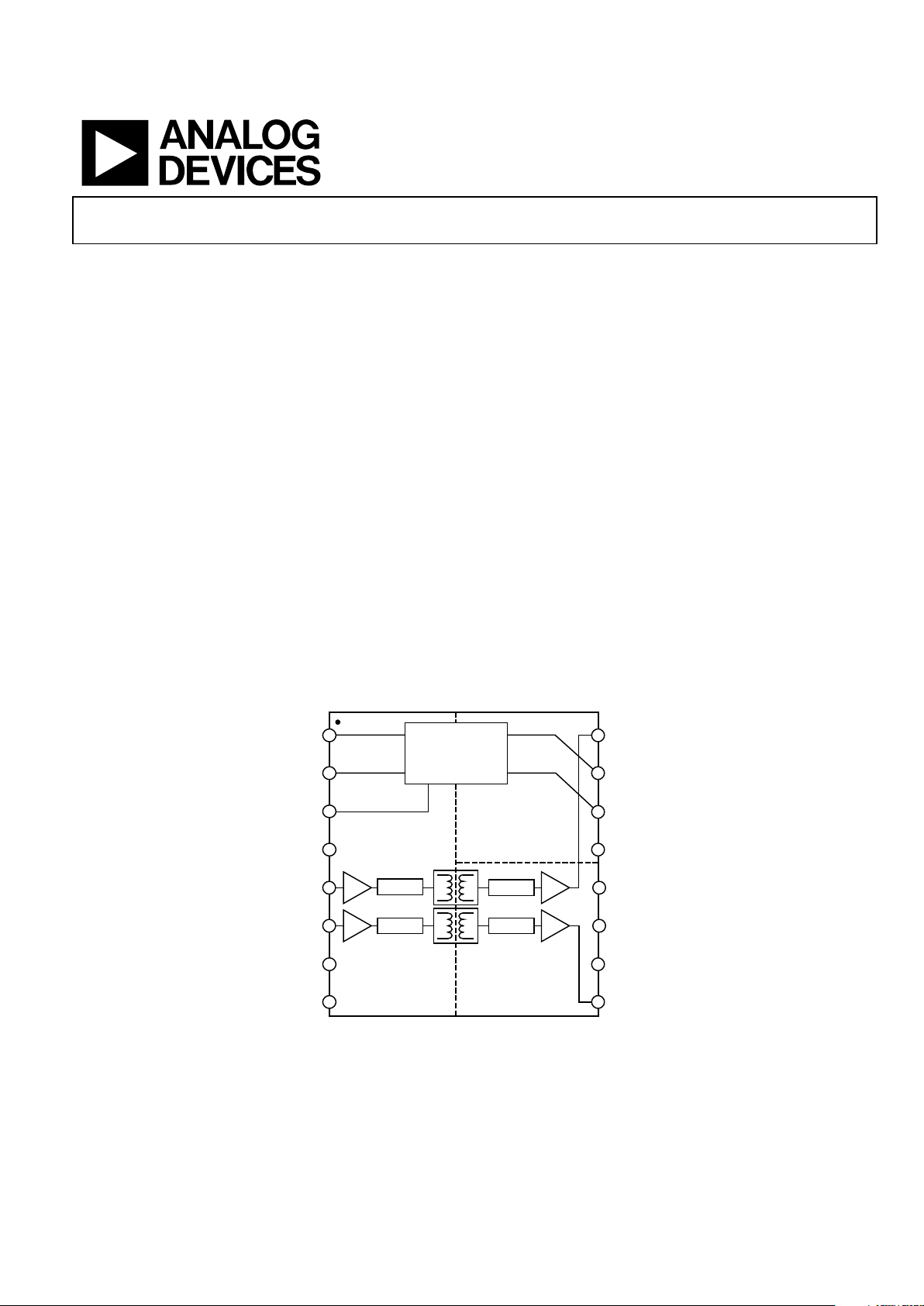
FUNCTIONAL BLOCK DIAGRAM
07080-001
V
DD1
7
V
DDB
10
GND
1
8
V
OB
9
V
DD1
3
GND
ISO
14
V
ADJ
4
NC
13
V
IA
5
NC
12
DECODE
ENCODE
V
IB
6
GND
B
11
DECODEENCODE
1
V
OA
16
GND
1
GND
1
2
V
ISO
15
ISOLATED
DC/DC
CONVERTER
╓
╜
╓
╜
╓
╜
╓
╜
NC = NO CONNECT
ADuM5230
Figure 1.

ADuM5230
Rev. 0 | Page 2 of 16
TABLE OF CONTENTS
Features .............................................................................................. 1
Applications ....................................................................................... 1
General Description ......................................................................... 1
Functional Block Diagram .............................................................. 1
Revision History ............................................................................... 2
Specifications ..................................................................................... 3
Electrical Characteristics ............................................................. 3
Package Characteristics ............................................................... 5
Regulatory Information ............................................................... 5
Insulation and Safety-Related Specifications ............................ 5
Recommended Operating Conditions ...................................... 5
Absolute Maximum Ratings ............................................................ 6
ESD Caution .................................................................................. 6
Pin Configuration and Pin Function Descriptions ...................... 7
Typical Perfomance Characteristics ................................................8
Applications Information .............................................................. 10
Theory of Operation .................................................................. 10
PC Board Layout ........................................................................ 10
Thermal Analysis ....................................................................... 10
Propagation Delay-Related Parameters ................................... 11
DC Correctness and Magnetic Field Immunity ........................... 11
Power Consumption .................................................................. 12
Increasing and Decreasing Available Power ............................... 12
Common-Mode Transient Immunity ..................................... 12
Typical Application Usage ......................................................... 13
Insulation Lifetime ..................................................................... 13
Outline Dimensions ....................................................................... 15
Ordering Guide .......................................................................... 15
REVISION HISTORY
4/08—Revision 0: Initial Version

ADuM5230
Rev. 0 | Page 3 of 16
SPECIFICATIONS
ELECTRICAL CHARACTERISTICS
All voltages are relative to their respective ground. 4.5 V ≤ V
DD1
≤ 5.5 V, 12.0 ≤ V
DDB
≤ 18.0 V. All min/max specifications apply over the
entire recommended operating range, unless otherwise noted. All typical specifications are at T
A
= 25°C, V
DD1
= 5.0 V, V
DDB
= 15 V.
Table 1.
Parameter Symbol Min Typ Max Unit Test Conditions
DC SPECIFICATIONS
Input Supply Current, Quiescent I
DD1(Q)
125 mA
I
ISO
= 0 mA, dc signal inputs,
V
ADJ
= open
Channel B Supply Current, Quiescent I
DDB(Q)
1.6 mA
Channel A Output Supply Voltage V
ISO
12 15 18.5 V
At 100 kHz Switching Frequency
Maximum Channel A Output Supply Current I
ISO(max, 100)
10 mA CL = 200 pF
Input Supply Current I
DD1
200 mA I
ISO
= I
ISO(max, 100)
Channel B Supply Current I
DDB
1.8 mA CL = 200 pF
At 1000 kHz Switching Frequency
Maximum Channel A Output Supply Current I
ISO(max, 1000)
7.5 mA CL = 200 pF
Input Supply Current I
DD1
200 mA I
ISO
= I
ISO(max, 1000)
Channel B Supply Current I
DDB
7.5 mA CL = 200 pF
Input Currents IIA, I
IB
−10 +0.01 +10 μA 0 ≤ VIA, VIB ≤ 5.5 V
Logic High Input Voltage V
ATH
, V
BTH
0.7 × V
DD1
V
Logic Low Input Voltage V
ATL
, V
BTL
0.3 × V
DD1
V
Logic High Output Voltages V
OAH
, V
OBH
V
ISO
– 0.1,
V
DDB
– 0.1
V
ISO
, V
DDB
V IOA, I
OB
= −1 mA
Logic Low Output Voltages V
OAL
, V
OBL
0.1 V IOA, I
OB
= 1 mA
Undervoltage Lockout, V
ISO
and V
DDB
Supply
Positive-Going Threshold V
DDBUV+
8.0 10.1 V
Negative-Going Threshold V
DDBUV−
7.4 9.0 V
Hysteresis V
DDBUVH
0.9 V
Undervoltage Lockout, V
DD1
Supply
Positive-Going Threshold V
DD1UV+
3.5 4.2 V
Negative-Going Threshold V
DD1UV−
3.0 3.9 V
Hysteresis V
DD1UVH
0.4 V
Output Short-Circuit Pulsed Current, Sourcing
1
I
OA
, IOB 100 mA
Output Short-Circuit Pulsed Current, Sinking
1
I
OA
, IOB 300 mA
SWITCHING SPECIFICATIONS
Minimum Pulse Width
2
PW 100 ns C
L
= 200 pF
Maximum Switching Frequency
3
1 MHz C
L
= 200 pF
Propagation Delay
4
t
PHL
, t
PLH
100 ns CL = 200 pF
Change vs. Temperature 100 ps/°C
Pulse Width Distortion, |t
PLH
− t
PHL
| PWD 8 ns CL = 200 pF
Channel-to-Channel Matching, Rising or Falling
Matching Edge Polarity
5
tM2 8 ns CL = 200 pF
Channel-to-Channel Matching, Rising vs. Falling
Opposite Edge Polarity
6
tM1 10 ns CL = 200 pF
Part-to-Part Matching, Rising or Falling Edges
7
55 ns C
L
= 200 pF
Part-to-Part Matching, Rising vs. Falling Edges
8
63 ns C
L
= 200 pF

ADuM5230
Rev. 0 | Page 4 of 16
Parameter Symbol Min Typ Max Unit Test Conditions
Common-Mode Transient Immunity
at Logic High Output
|CM
H
| 25 35 kV/μs
V
Ix
= V
DD1
, VCM = 1000 V,
transient magnitude = 800 V
Common-Mode Transient Immunity
at Logic Low Output
|CM
L
| 25 35 kV/μs
V
Ix
= 0 V, VCM = 1000 V,
transient magnitude = 800 V
Output Rise Time (10% to 90%) tR 25 ns
C
L
= 200 pF, I
ISO
= 10 mA,
100 kHz switching frequency
Output Fall Time (10% to 90%) tF 10 ns
C
L
= 200 pF, I
ISO
= 10 mA,
100 kHz switching frequency
1
Short-circuit duration is less than 1 sec. Average output current must conform to the limit shown under the section. Absolute Maximum Ratings
2
The minimum pulse width is the shortest pulse width at which the specified timing parameters are guaranteed. Operation below the minimum pulse width is strongly
discouraged because in some instances pulse stretching to 1 μs may occur.
3
The maximum switching frequency is the maximum signal frequency at which the specified timing and power conversion parameters are guaranteed. Operation
above the maximum frequency is strongly discouraged.
4
t
PHL
propagation delay is measured from the 50% level of the falling edge of the VIx signal to the 50% level of the falling edge of the VOx signal. t
PLH
propagation delay is
measured from the 50% level of the rising edge of the VIx signal to the 50% level of the rising edge of the VOx signal.
5
In channel-to-channel matching, the rising or falling matching edge polarity is the magnitude of the propagation delay difference between two channels of the same
part when both inputs are either both rising or falling edges. The loads on each channel are equal.
6
In channel-to-channel matching, the rising vs. falling opposite edge polarity is the magnitude of the propagation delay difference between two channels of the same
part when one input is a rising edge and one input is a falling edge. The loads on each channel are equal.
7
In part-to-part matching, the rising or falling edges is the magnitude of the propagation delay difference between the same channels of two different parts when the
inputs are either both rising or falling edges. The supply voltages, temperatures, and loads of each part are equal.
8
In part-to-part matching, the rising vs. falling edges is the magnitude of the propagation delay difference between the same channels of two different parts when one
input is a rising edge and the other input is a falling edge. The supply voltages, temperatures, and loads of each part are equal.
ADuM5230
Rev. 0 | Page 5 of 16
PACKAGE CHARACTERISTICS
Table 2.
Parameter Symbol Min Typ Max Unit Test Conditions
Resistance (Input-to-Output)
1
R
I-O
1012 Ω
Capacitance (Input-to-Output)
1
C
I-O
2.0 pF f = 1 MHz
Input Capacitance CI 4.0 pF
IC Junction-to-Ambient Thermal Resistance θJA 48 °C/W
1
The device is considered a two-terminal device: Pin 1 to Pin 8 are shorted together, and Pin 9 to Pin 16 are shorted together.
REGULATORY INFORMATION
The ADuM5230 will be approved by the organization listed in Tab l e 3.
Table 3.
UL1 (pending)
Recognized under 1577 component recognition program, File E214100
1
In accordance with UL1577, each ADuM5230 is proof-tested by applying an insulation test voltage ≥3000 V rms for 1 sec (current leakage detection limit = 5 μA).
INSULATION AND SAFETY-RELATED SPECIFICATIONS
Table 4.
Parameter Symbol Value Unit Conditions
Rated Dielectric Insulation Voltage
2500 V rms
1 minute duration
Minimum External Air Gap (Clearance)
L(I01) 3.5 min mm
Measured from input conductors to output conductors,
shortest distance through air
Minimum External Tracking (Creepage)
L(I02) 3.5 min mm
Measured from input conductors to output conductors,
shortest distance path along body
Minimum Internal Gap (Internal
Clearance)
0.017 min mm
Distance through the insulation
Tracking Resistance (Comparative
Tracking I ndex)
CTI >175
V
DIN IEC 112/VDE 0303 Part 1
Isolation Group
IIIa
Material Group (DIN VDE 0110, 1/89, Table 1)
600
500
400
300
200
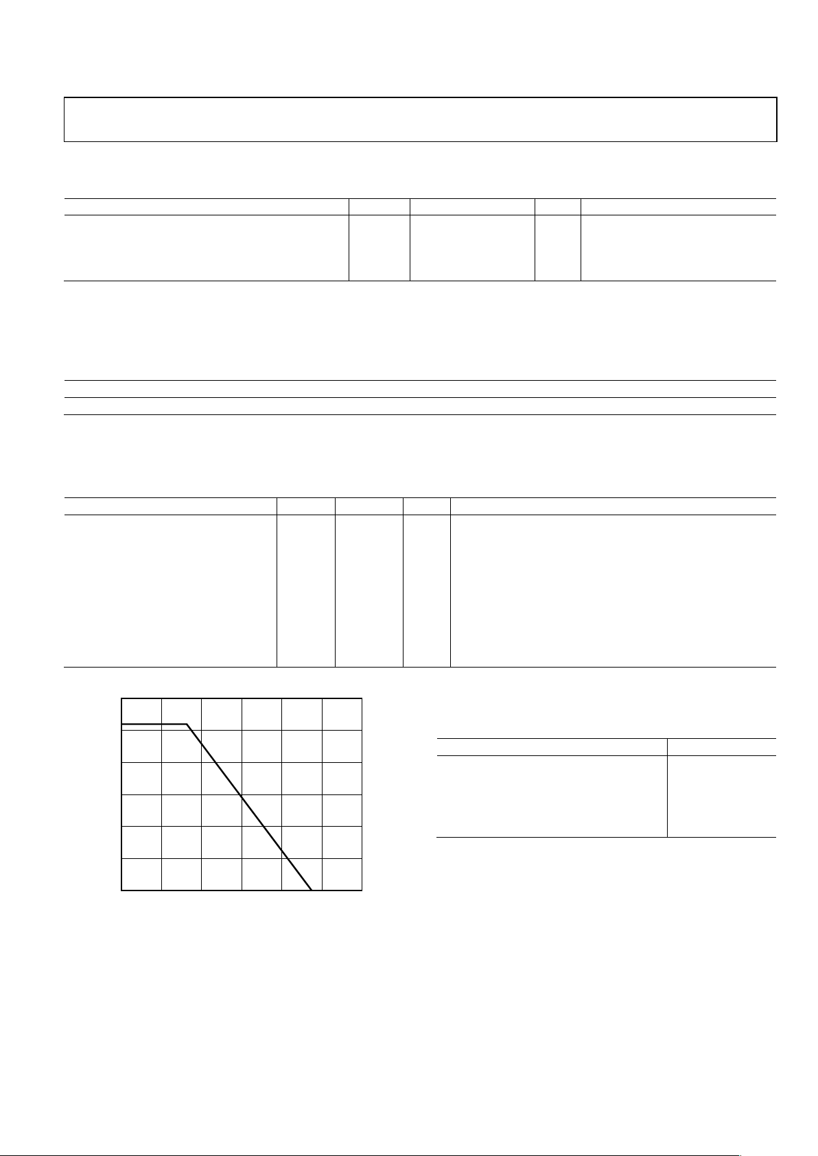
100
0
–40 0 40 80 120 160 200
AMBIENT TEMPERATURE (°C)
SAFE OPERATING V
DD1
CURRENT (mA)
07080-010
Figure 2. Thermal Derating Curve, Dependence of Safety Limiting Values on
Case Temperature, per DIN EN 60747-5-2
RECOMMENDED OPERATING CONDITIONS
Table 5.
Parameter Value
Operating Temperature (TA) −40°C to +105°C
Input Supply Voltage1 (V
DD1
) 4.5 V to 5.5 V
Channel B Supply Voltage1 (V
DDB
) 12 V to 18.5 V
Input Signal Rise and Fall Times 1 ms
Minimum V
DD1
Power-On Slew Rate2 (P
SLEW
) 400 V/ms
1
All voltages are relative to their respective ground.
2
The ADuM5230 power supply may fail to initialize properly if V
DD1
is applied
too slowly.

ADuM5230
Rev. 0 | Page 6 of 16
ABSOLUTE MAXIMUM RATINGS
Ambient temperature = 25°C, unless otherwise noted.
Table 6.
Parameter Rating
Storage Temperature (TST) −55°C to +150°C
Ambient Operating Temperature (TA) −40°C to +105°C
Input Supply Voltage1 (V
DD1
) −0.5 V to +7.0 V
Channel B Supply Voltage1 (V
DDB
) −0.5 V to +27 V
Input Voltage1 (VIA, VIB) −0.5 V to V
DDI
+ 0.5 V
Output Voltage1 (VOA, VOB)
−0.5 V to V
ISO
+ 0.5 V,
−0.5 V to V
DDB
+ 0.5 V
Input-Output Voltage
2
−700 V
PEAK
to +700 V
PEAK
Output Differential Voltage
3
700 V
PEAK
Output DC Current (IOA, IOB) −20 mA to +20 mA
Common-Mode Transients
4
−100 kV/μs to +100 kV/μs
1
All voltages are relative to their respective ground.
2
Input-to-output voltage is defined as GND
ISO
− GND1 or GNDB − GND1.
3
Output differential voltage is defined as GND
ISO
− GNDB.
4
Refers to common-mode transients across any insulation barrier. Common-
mode transients exceeding the Absolute Maximum Ratings may cause
latch-up or permanent damage.
Stresses above those listed under Absolute Maximum Ratings
may cause permanent damage to the device. This is a stress
rating only; functional operation of the device at these or any
other conditions above those listed in the operational sections
of this specification is not implied. Exposure to absolute
maximum rating conditions for extended periods may affect
device reliability.
ESD CAUTION
Table 7. Maximum Continuous Working Voltage
1
Parameter Max Unit Constraint
AC Voltage, Bipolar Waveform 424 V peak
50-year minimum lifetime
AC Voltage, Unipolar Waveform
Basic Insulation 600 V peak
50-year minimum lifetime
DC Voltage
Basic Insulation 600 V peak
50-year minimum lifetime
1
Refers to continuous voltage magnitude imposed across the isolation barrier. See the Insulation Lifetime section for more details.

ADuM5230
Rev. 0 | Page 7 of 16
PIN CONFIGURATION AND PIN FUNCTION DESCRIPTIONS
G
ND
1
1
V
DD1
2
V
ADJ
3
G
ND
1
4
V
OA
16
V
ISO
15
GND
ISO
14
NC
13
V
IA
5
NC
12
V
6
IB
GND
11
B
V
DD1
7
V
DDB
10
G
ND
1
8
V
OB
9
NC = NO CONNECT
ADuM5230
TOP VIEW
(Not to S cale)
07080-002
Figure 3. Pin Configuration
Table 8. Pin Function Descriptions
Pin No. Mnemonic Description
1 GND
1
Ground Reference for Input Logic Signals.
2 V
DD1
Input Supply Voltage, 4.5 V to 5.5 V.
3 V
ADJ
Adjusts Internal DC-to-DC Converter Duty Cycle (Normally Left Unconnected).
4 GND
1
Ground Reference for Input Logic Signals.
5 V
IA
Logic Input A.
6 V
IB
Logic Input B.
7 V
DD1
Input Supply Voltage, 4.5 V to 5.5 V.
8 GND
1
Ground Reference for Input Logic Signals.
9 VOB Output B Signal.
10 V
DDB
Output B Supply Voltage, 12 V to 18 V.
11 GND
B
Ground Reference for Output B Signal.
12 NC No Connect.
13 NC No Connect.
14 GND
ISO
Ground Reference for Output A Signal and Isolated Output Supply Voltage.
15 V
ISO
Isolated Output Supply Voltage.
16 VOA Output A Signal.
Table 9. Truth Table (Positive Logic)
VIA
Input
VIB
Input
V
DD1
State
1
V
ISO
State1V
DDB
State
1
VOA
Output
VOB
Output Notes
High High Powered Powered Powered High High
High Low Powered Powered Powered High Low
Low High Powered Powered Powered Low High
Low Low Powered Powered Powered Low Low
X X UVLO Unpowered X Low Low
Output returns to input state within 1 μs of V
DD1
power restoration.
X X Powered UVLO Unpowered Low Low
Output returns to input state within 1 μs of V
ISO
and V
DDB
power restoration.
X High Powered UVLO Powered Low High
Output returns to input state within 1 μs of V
ISO
power restoration.
X Low Powered UVLO Powered Low Low
Output returns to input state within 1 μs of V
ISO
power restoration.
High X Powered Powered UVLO High Low
V
OB
output returns to input state within 1 μs of
V
DDB
power restoration.
Low X Powered Powered UVLO Low Low
V
OB
output returns to input state within 1 μs of
V
DDB
power restoration.
1
UVLO represents either a voltage below the UVLO threshold for that supply or absence of power.

ADuM5230
Rev. 0 | Page 8 of 16
TYPICAL PERFOMANCE CHARACTERISTICS
20
19
18
17
16
15
14
13
12
11
10
0 5 10 15 20
I
ISO
LOAD CURRENT (mA)
V
ISO
(V)
07080-011
4.5V
5.0V
5.5V
Figure 4. Typical V
ISO
Supply Voltage vs. I
ISO
External Load Current
200
180
160
140
120
100
80
60
40
20
0
0 5 10 15 20
I
ISO
LOAD CURRENT (mA)
I
DD1
CURRENT (mA)
07080-012
4.5V
5.0V
5.5V
Figure 5. Typical V
DD1
Supply Current vs. V
ISO
External Load Current
30
25
20
15
10
5
0
0 5 10 15 20
I
ISO
LOAD CURRENT (mA)
EFFICIENCY (%)
07080-013
4.5V
5.0V
5.5V
Figure 6. Typical V
ISO
Supply Efficiency vs. V
ISO
External Load Current
14.0
13.5
13.0
12.5
12.0
11.5
11.0
–40 0 40 80 120
TEMPERATURE (° C)
V
ISO
@ MAXIMUM LOAD (V)
07080-014
V
ISO
@ 100kHz
V
ISO
@ 1MHz
Figure 7. Typical V
ISO
Output Voltage at Maximum Combined Load Over
Temperature
6
5
4
3
2
1
0
0 200 400 600 800 1000
FREQUENCY (kHz)
V
DDB
(mA)
07080-015
18V
15V
12V
Figure 8. Typical Current Consumption for VOA or VOB Outputs, CL = 200 pF
0
–0.5
–1.0
–1.5
–2.0
–2.5
–3.0
0 50 100 150 200
I
OH
(mA)
(
V
OH
–
V
DD
) OUTPUT VOLTAGE DRO P (V)
07080-016
Figure 9. Typical VOH Drop vs. IOH (V
DD1
= 5 V, V
DDB
, V
ISO
= 12 V to 18 V)

ADuM5230
Rev. 0 | Page 9 of 16
2.0
1.5
1.0
0.5
0
0 100 200 300 40 0
I
OL
(mA)
V
OL
OUTPUT VO LTAGE (V)
07080-017
Figure 10. Typical VOL vs. IOL (V
DD1
= 5 V, V
DDB
, V
ISO
= 12 V to 18 V)
70
68
66
64
62
60
–40 0 40 80 120
TEMPERATURE (°C)
PROPAGATI ON DELAY (n s)
07080-018
TPLH @ 18V
TP
HL
@ 18V
TP
LH
@ 12V
TP
HL
@ 12V
Figure 11. Typical Propagation Delay vs. Temperature
1600
1400
1200
1000
800
600
400
200
0
1 10 100 1000
LOAD IMPEDANCE ( Ω)
POWER DISSIPATION (mW)
07080-019
V
DD1
= 5.5V
V
DD1
= 4.5V
Figure 12. Power Dissipation vs. Load Impedance for Fault Conditions
40
35
30
25
20
15
10
5
0
0 2040608010
PWM DUTY FACTOR (%)
OUTPUT CURRENT (mA)
07080-020
0
V
ISO
= 15V
V
ISO
= 12V
Figure 13. Current Available at the Output vs. PWM Duty Factor for V
DD1
= 5 V
1.0
0.9
0.8
0.7
0.6
0.5
0.4
0.3
0.2
0.1
0
0/10 1/9 2/8 3/7 4/6 5/ 5 6/4 7/3
UPPER/ LOWE R V
ADJ
RESISTOR VALUES (kΩ)
ON DUTY FACTO R
07080-021
V
DD1
= 5.0
Figure 14. Upper/Lower V
ADJ
Voltage Divider Resistor Values to Determine
PWM Duty Factor for V
DD1
= 5 V

ADuM5230
Rev. 0 | Page 10 of 16
APPLICATIONS INFORMATION
THEORY OF OPERATION
The dc-to-dc converter section of the ADuM5230 works on
principles that are common to most modern power supply
designs. It is implemented as an open-loop PWM controller,
which sets the power level being transferred to the secondary.
V
DD1
power is supplied to an oscillating circuit that switches
current into a chip-scale air core transformer. On the secondary
side, power is rectified to a dc voltage. The voltage is then
clamped to approximately 18 V and provided to the secondary
side V
OA
data channel and to the V
ISO
pin for external use. The
output voltage is unregulated and varies with load.
The PWM duty cycle is set by internal bias elements, but can be
controlled externally through the V
ADJ
pin with an external
resistor network. This feature allows the user to boost the
available power at the secondary, or reduce excess power if it is
not required for the application (see the Power Consumption
section).
Undervoltage lockouts are provided on the V
DD1
, V
DDB
, and V
ISO
supply lines to interlock the data channels from low supply
voltages.
PC BOARD LAYOUT
The ADuM5230 digital isolator with a 150 mW isoPower™
integrated dc-to-dc converter requires no external interface
circuitry for the logic interfaces. Power supply bypassing is
required at the input and output supply pins (see Figure 15).
The power supply section of the ADuM5230 uses a very high
oscillator frequency to pass power efficiently through its chip
scale transformers. In addition, the normal operation of the
data section of the iCoupler® introduces switching transients on
the power supply pins. Bypass capacitors are required for
several operating frequencies. Noise suppression requires a low
inductance high frequency capacitor; ripple suppression and
proper regulation require a large value capacitor. These are most
conveniently connected between Pin 1 and Pin 2 for V
DD1
and
between Pin 15 and Pin 14 for V
ISO
. To suppress noise and
reduce ripple, a parallel combination of at least two capacitors is
required. The recommended capacitor values are 0.1 µF and
10 µF. It is strongly recommended that a very low inductance
ceramic or equivalent capacitor be used for the smaller value.
The total lead length between both ends of the capacitor and
the input power supply pin should not exceed 20 mm.
Bypassing with noise suppression and stiffening capacitors is
recommended between Pin 1 and Pin 2, a bypass capacitor is
recommended between Pin 7 and Pin 8. Bypassing with noise
suppression and stiffening capacitors is recommended between
Pin 14 and Pin 15.
GND
1
V
DD1
V
ADJ
GND
1
V
OA
V
ISO
GND
ISO
NC
V
IA
NC
V
IB
GND
B
V
DD1
V
DDB
GND
1
V
OB
07080-022
NC = NO CONNECT
ADuM5230
TOP VIEW
(Not to S cale)
Figure 15. Recommended Printed Circuit Board Layout
In applications involving high common-mode transients, care
should be taken to ensure that board coupling across the isolation
barrier is minimized. Furthermore, the board layout should be
designed such that any coupling that does occur equally affects
all pins on a given component side. Failure to ensure this may
cause voltage differentials between pins exceeding the absolute
maximum ratings specified in Ta b l e 6, leading to latch-up
and/or permanent damage.
The ADuM5230 is a power device that dissipates about 1 W of
power when fully loaded and run at maximum speed. Because it
is not possible to apply a heat sink to an isolation device, the device
primarily depends on heat dissipation into the PCB through the
GND pins. If the device is used at high ambient temperatures,
care should be taken to provide a thermal path from the GND
pins to the PCB ground plane. The board layout in Figure 15
shows enlarged pads for Pin 1 and Pin 8. Multiple vias should
be implemented from the pad to the ground plane. This significantly reduces the temperatures inside the chip. The dimensions
of the expanded pads are left to the discretion of the designer
and the available board space.
THERMAL ANALYSIS
The ADuM5230 part consists of several internal die attached to
three lead frames, each with a die attach paddle. For the purposes
of thermal analysis, the device is treated as a thermal unit with
the highest junction temperature reflected in the θ
JA
parameter
shown in Tab l e 2. The value of θ
JA
is based on measurements
taken with the part mounted on a JEDEC standard four-layer
board with fine width traces and still air. Under normal operating
conditions, the ADuM5230 operates at full load across the full
temperature range without derating the output current.
However, following the recommendations in the PC Board
Layout section decreases the thermal resistance to the PCB,
allowing increased thermal margin in high ambient
temperatures.
Under output short-circuit conditions, as shown in Figure 12,
the package power dissipation is within safe operating limits;
however, if the load is in the 100 range, power dissipation is
high enough to cause thermal damage when the ambient temperature is above 80°C. Care should be taken to avoid excessive
nonshort loads if the part is to be operated at high temperatures.

ADuM5230
Rev. 0 | Page 11 of 16
PROPAGATION DELAY-RELATED PARAMETERS
Propagation delay is a parameter that describes the time it takes
a logic signal to propagate through a component. The propagation
delay to a logic low output may differ from the propagation
delay to a logic high.
INPUT (
V
Ix
)
OUTPUT (V
Ox
)
t
PLH
t
PHL
50%
50%
07080-023
Figure 16. Propagation Delay Parameters
Pulse width distortion is the maximum difference between
these two propagation delay values and is an indication of how
accurately the input signal timing is preserved.
Channel-to-channel matching refers to the maximum amount
the propagation delay differs between channels within a single
ADuM5230 component.
DC CORRECTNESS AND MAGNETIC FIELD IMMUNITY
Positive and negative logic transitions at the isolator input
cause narrow (~1 ns) pulses to be sent to the decoder via the
transformer. The decoder is bistable and is, therefore, either set
or reset by the pulses, indicating input logic transitions. In the
absence of logic transitions at the input for more than 1 µs, a
periodic set of refresh pulses indicative of the correct input state
are sent to ensure dc correctness at the output. If the decoder
receives no internal pulses of more than about 5 µs, the input
side is assumed to be unpowered or nonfunctional, in which
case the isolator output is forced to a default state (see Tab l e 9 )
by the watchdog timer circuit.
The limitation on the ADuM5230 magnetic field immunity is set
by the condition in which induced voltage in the transformer
receiving coil is sufficiently large to either falsely set or reset the
decoder. The following analysis defines the conditions under
which this may occur.
The pulses at the transformer output have an amplitude greater
than 1.0 V. The decoder has a sensing threshold at about 0.5 V, thus
establishing a 0.5 V margin in which induced voltages can be
tolerated. The voltage induced across the receiving coil is given by
V =
(
; n = 1, 2, … , N
)
2π/
n
rdtd∑=
β
where:
β is magnetic flux density (gauss).
N is the number of turns in the receiving coil.
r
n
is the radius of the nth turn in the receiving coil (cm).
Given the geometry of the receiving coil in the ADuM5230 and
an imposed requirement that the induced voltage be at most
50% of the 0.5 V margin at the decoder, a maximum allowable
magnetic field is calculated, as shown in Figure 17.
MAGNETIC FIELD FREQUENCY (Hz)
100
MAXIMUM ALLOWABLE MAGNETIC FLUX
DENSITY (kgauss)
0.001
1M
10
0.01
1k 10k 10M
0.1
1
100M100k
07080-024
Figure 17. Maximum Allowable External Magnetic Flux Density
For example, at a magnetic field frequency of 1 MHz, the
maximum allowable magnetic field of 0.2 kgauss induces a
voltage of 0.25 V at the receiving coil. This is about 50% of the
sensing threshold and does not cause a faulty output transition.
Similarly, if such an event occurs during a transmitted pulse
(and was of the worst-case polarity), it would reduce the
received pulse from >1.0 V to 0.75 V, still well above the 0.5 V
sensing threshold of the decoder.
The preceding magnetic flux density values correspond to
specific current magnitudes at given distances from the
ADuM5230 transformers. Figure 18 expresses these allowable
current magnitudes as a function of frequency for selected
distances. As shown, the ADuM5230 is extremely immune and
can be affected only by extremely large currents operated at
high frequency very close to the component. For the 1 MHz
example noted, the user would have to place a 0.5 kA current
5 mm away from the ADuM5230 to affect the operation of the
component.
MAGNETIC F IELD FREQ UENCY (Hz)
MAXIMUM ALL OWABLE CURRENT (kA)
1000
100
10
1
0.1
0.01
1k 100M100k10k 1M 10M
DISTANCE = 5mm
DISTANCE = 1m
DISTANCE = 100mm
07080-025
Figure 18. Maximum Allowable Current
for Various Current-to-ADuM5230 Spacings
Note that at combinations of strong magnetic field and high
frequency, any loops formed by PCB traces may induce error
voltages sufficiently large enough to trigger the thresholds of

ADuM5230
Rev. 0 | Page 12 of 16
succeeding circuitry. Care should be taken in the layout of such
traces to avoid this possibility.
POWER CONSUMPTION
The power converter in the ADuM5230 provides 13 mA of
power to the secondary in its default configuration. Power is
provided to both the data channel, V
OA
, and the V
ISO
pin for off-
chip use. Current consumption of V
OA
varies with frequency as
shown in Figure 8. The maximum available power for external
use decreases as the frequency of the data channel increases to
stay within the total available current.
INCREASING AND DECREASING AVAILABLE POWER
The V
ADJ
pin is used to increase or decrease the available power
at the V
ISO
pin. This allows the increase of the V
ISO
voltage for a
given load or the increase of the maximum V
ISO
load. Alternatively,
power can also be reduced when it is not required at the output,
lowering the quiescent current and saving power.
Power adjustment is accomplished by adding a voltage divider
between V
ADJ
, V
DD1
and GND as shown in Figure 25. Under
normal operation, the V
ADJ
pin is left open, allowing the internal
bias network to set the duty factor of the internal PWM. If the
V
ADJ
pin is connected via a resistor divider, a duty factor other
than the default can be chosen. The relationship between the
duty factor of the internal PWM and the available power under
load is shown in Figure 13. When the desired duty factor is
chosen, the values of the upper and lower divider resistors can
be chosen as shown in Figure 14, which assumes a 10 kΩ total
divider resistance.
COMMON-MODE TRANSIENT IMMUNITY
In general, common-mode transients consist of linear and
sinusoidal components. The linear component of a commonmode transient is given by
V
CM, linear
= (V/t) t
where V/t is the slope of the transient shown in Figure 19
and Figure 20.
The transient of the linear component is given by
dV
CM
/dt = V/t
The ability of the ADuM5230 to operate correctly in the
presence of linear transients is characterized by the data in
Figure 22. The data is based on design simulation and is the
maximum linear transient magnitude that the ADuM5230 can
tolerate without an operational error. This data shows a higher
level of robustness than what is shown in Ta b le 1 because the
transient immunity values obtained in Tabl e 1 use measured
data and apply allowances for measurement error and margin.
GND
1
V
DD1
ΔV
Δt
ΔV
Δt
5V
GND
1
V
DD1
15V
15V
GND
ISO
AND GND
B
V
ISO
AND V
DDB
5V
GND
ISO
AND GND
B
V
ISO
AND V
DDB
15V
15V
07080-006
Figure 19. Common-Mode Transient Immunity Waveforms—Input to Output
GNDB/GND
B
V
ISO/VDDB
ΔV
Δt
ΔV
Δt
15V
GNDB/GND
B
V
ISO/VDDB
15V
15V
GND
ISO
/GND
B
V
ISO/VDDB
15V
GND
ISO
/GND
B
V
ISO/VDDB
15V
15V
07080-007
Figure 20. Common-Mode Transient Immunity Waveforms—Between Outputs
GND
ISO
/GND
B
V
ISO/VDDB
V
ISO/VDDB
GND
ISO
/GND
B
07080-008
ΔV
DD
Δt
Figure 21. Transient Immunity Waveforms—Output Supplies

ADuM5230
Rev. 0 | Page 13 of 16
07080-003
TEMPERATURE (°C )
100–40 0 40 80–20 20 60
TRANSIENT I MMUNITY (kV/µs)
300
250
200
150
100
50
0
WORST-CASE PROCESS VARIATION
BEST-CASE PROCESS VARIATION
Figure 22. Transient Immunity (Linear Transients) vs. Temperature
The sinusoidal component (at a given frequency) is given by
V
CM, sinusoidal
= V0sin(2πft)
where:
V
0
is the magnitude of the sinusoidal.
f is the frequency of the sinusoidal.
The transient magnitude of the sinusoidal component is given by
dV
CM
/dt = 2πf V
0
The ability of the ADuM5230 to operate correctly in the presence of sinusoidal transients is characterized by the data in
Figure 23 and Figure 24. The data is based on design simulation
and is the maximum sinusoidal transient magnitude (2πf V
0
)
that the ADuM5230 can tolerate without an operational error.
Values for immunity against sinusoidal transients are not
included in Tabl e 1 because measurements to obtain such values
have not been possible.
07080-004
FREQUENCY ( MHz)
20000 500 1000 1500 1750250 750 1250
TRANSIENT I MMUNITY (kV/µs)
200
160
180
120
80
40
140
100
60
20
0
WORST-CASE PROCESS VARIATION
BEST-CASE PROCESS VARIATION
Figure 23. Transient Immunity (Sinusoidal Transients),
27°C Ambient Temperature
07080-005
FREQUENCY ( MHz)
20000 500 1000 1500 1750250 750 1250
TRANSIENT IMMUNITY (kV/µs)
200
140
100
60
20
160
180
120
80
40
0
WORST-CASE PROCESS VARIATION
BEST-CASE PROCESS VARIATION
Figure 24. Transient Immunity (Sinusoidal Transients),
100°C Ambient Temperature
TYPICAL APPLICATION USAGE
The ADuM5230 is intended for driving low gate capacitance
transistors (200 pF typically). Most high voltage applications
involve larger transistors than this. To accommodate these
applications, users can implement a buffer configuration with
the ADuM5230, as shown in Figure 25. In many cases, the
buffer configuration is the least expensive option and provides
the greatest amount of design flexibility. The precise buffer/high
voltage transistor combination can be selected to fit the needs of
the application.
07080-009
+H
V
–HV
GND
1
V
DD1
V
ADJ
V
IA
V
ISO
V
OA
GND
ISO
V
DDB
V
OB
GND
B
V
IB
ADuM5230
FLOATING V
DDB
R
UPPER
R
LOWER
Figure 25. Application Circuit
INSULATION LIFETIME
All insulation structures eventually break down when subjected
to voltage stress over a sufficiently long period. The rate of
insulation degradation depends on the characteristics of the
voltage waveform applied across the insulation. In addition to
the testing performed by the regulatory agencies, Analog
Devices conducts an extensive set of evaluations to determine
the lifetime of the insulation structure within the ADuM5230.
Analog Devices performs accelerated life testing using voltage
levels higher than the rated continuous working voltage.
Acceleration factors for several operating conditions are
determined. These factors allow calculation of the time to
failure at the actual working voltage. Tabl e 7 summarizes the
peak voltages for 50 years of service life for a bipolar ac
operating condition and the maximum Analog Devices

ADuM5230
Rev. 0 | Page 14 of 16
0V
RATED PEAK VOLTAGE
07080-026
recommended working voltages. In many cases, the approved
working voltage is higher than the 50-year service life voltage.
Operation at these high working voltages can lead to shortened
insulation life in some cases.
Figure 26. Bipolar AC Waveform
The insulation lifetime of the ADuM5230 depends on the
voltage waveform type imposed across the isolation barrier.
The iCoupler insulation structure degrades at different rates
depending on whether the waveform is bipolar ac, unipolar ac,
or dc. Figure 26, Figure 27, and Figure 28 illustrate these
different isolation voltage waveforms.
0V
RATED PEAK VOLTAGE
07080-027
Figure 27. Unipolar AC Waveform
Bipolar ac voltage is the most stringent environment. The goal
of a 50-year operating lifetime under the ac bipolar condition
determines the maximum working voltage recommended by
Analog Devices.
0V
RATED PEAK VOLTAGE
07080-028
In the case of unipolar ac or dc voltage, the stress on the insulation is significantly lower. This allows operation at higher
working voltages while still achieving a 50-year service life.
The working voltages listed in Tab l e 7 can be applied while
maintaining the 50-year minimum lifetime, provided the
voltage conforms to either the unipolar ac or dc voltage cases.
Any cross insulation voltage waveform that does not conform to
Figure 27 or Figure 28 should be treated as a bipolar ac waveform,
and its peak voltage should be limited to the 50-year lifetime
voltage value listed in Tab l e 7. Note that the voltage presented in
Figure 27 is shown as sinusoidal for illustration purposes only.
It is meant to represent any voltage waveform varying between
0 V and some limiting value. The limiting value can be positive
or negative, but the voltage cannot cross 0 V.
Figure 28. DC Waveform

ADuM5230
Rev. 0 | Page 15 of 16
OUTLINE DIMENSIONS
CONTROLL ING DIMENSI ONS ARE IN MILLIMET ERS; INCH DIM ENSIONS
(IN PARENTHESES) ARE ROUNDED-O FF MILLIMETER EQ UIVALENTS FOR
REFERENCE ONLY AND ARE NOT APPROPRI ATE FOR USE IN DESI GN.
COMPLIANT TO JEDEC STANDARDS MS-013- AA
032707-B
10.50 (0.4134)
10.10 (0.3976)
0.30 (0.0 118)
0.10 (0.0039)
2.65 (0.1043)
2.35 (0.0925)
10.65 (0.4193)
10.00 (0.3937)
7.60 (0.2992)
7.40 (0.2913)
0
.
7
5
(
0
.
0
2
9
5
)
0
.
2
5
(
0
.
0
0
9
8
)
45°
1.27 (0.0500)
0.40 (0.0157)
C
OPLANARITY
0.10
0.33 (0.0130)
0.20 (0.0079)
0.51 (0.0201)
0.31 (0.0122)
SEATING
PLANE
8°
0°
16
9
8
1
1.27 (0.0500)
BSC
Figure 29. 16-Lead Standard Small Outline Package [SOIC_W]
Wide Body
(RW-16)
Dimensions shown in millimeters (inches)
ORDERING GUIDE
Model
No. of
Channels
Output Peak
Current (A)
1
Output
Voltage (V) Temperature Range Package Description
Package
Option
ADuM5230ARWZ
2
2 0.1/0.3 15 −40°C to +105°C 16-Lead SOIC_W RW-16
ADuM5230ARWZ-RL
2
2 0.1/0.3 15 −40°C to +105°C
16-Lead SOIC_W, 13-inch Tape
and Reel Option (1,000 Units)
RW-16
1
Sourcing/sinking.
2
Z = RoHS Compliant Part.

ADuM5230
Rev. 0 | Page 16 of 16
NOTES
©2008 Analog Devices, Inc. All rights reserved. Trademarks and
registered trademarks are the property of their respective owners.
D07080-0-4/08(0)
 Loading...