

Page 1
查询EVAL-AD7891-1CB供应商
Evaluation Board for Single Supply,
a
FEATURES
Full-Featured Evaluation Board for the AD7891-1
EVAL-CONTROL BOARD Compatible
Stand Alone Capability
On-Board Analog Buffering and Reference
Various Linking Options
PC Software for Control and Data Analysis when used
with EVAL-CONTROL BOARD
INTRODUCTION
This Application Note describes the evaluation board for the
AD7891-1 12-Bit A/D converter. The AD7891 is an eight
channel data acquisition system that operates from a single +5 V
supply and accepts input signals in the range ±5 V or ±10 V. It
incorporates an input multiplexer, an on chip track/hold
amplifier, an internal +2.5 V reference and on-chip versatile
interface structures that allow both serial and parallel connection to a microprocessor. This flexible serial interface allows the
AD7891-1 to connect directly to Digital Signal Processors
(ADSP-2101, DSP56001, etc.) and Microcontrollers (8XC51,
68HC11, etc.). Full data on the AD7891-1 is available in the
AD7891 data sheet available from Analog Devices and should
be consulted in conjunction with this Application Note when
using the Evaluation Board.
On-board components include an AD780 which is a pin
programmable +2.5 V ultra high precision bandgap reference,
and two AD713 quad op-amps to buffer the analog inputs.
12-Bit 454 kSPS ADC
EVAL-AD7891-1CB
Interfacing to this board is through a 9-way D-type connector
and a 96-way connector. This 96-way connector is compatible
with the EVAL-CONTROL BOARD which is also available
from Analog Devices. External sockets are provided for the
conversion start input, analog inputs and an external reference
input option.
OPERATING THE AD7891-1 EVALUATION BOARD
Power Supplies
This evaluation board has four analog power supply inputs:
, DGND, +12 V and -12 V. The VDD supply is nominally
V
DD
+5 V and is used to power the AD7891-1 and the on-board
digital integrated circuits. The +12 V and -12 V supplies are
used to power the AD713 quad op-amps and the AD780 voltage
reference. The DGND connection is to the digital ground
plane. This DGND ground plane connects to the AGND
ground plane at the AD7891-1. Therefore, it is recommended
not to connect AGND and DGND elsewhere in the system.
The various analog and digital supplies are provided through the
power-supply terminals on the board. When using the AD78911 evaluation board with the EVAL-CONTROL BOARD, all
supplies are provided by the EVAL-CONTROL BOARD.
All supplies are decoupled to ground with 10 µF tantalum and
0.1 µF ceramic disc capacitors. The +12 V and -12 V supplies
for the amplifiers are decoupled to the AGND plane while the
supply for the AD7891 is decoupled to the AGND plane
AV
DD
through a 10 µF capacitor and to the DGND plane through a
0.1 µF capacitor.
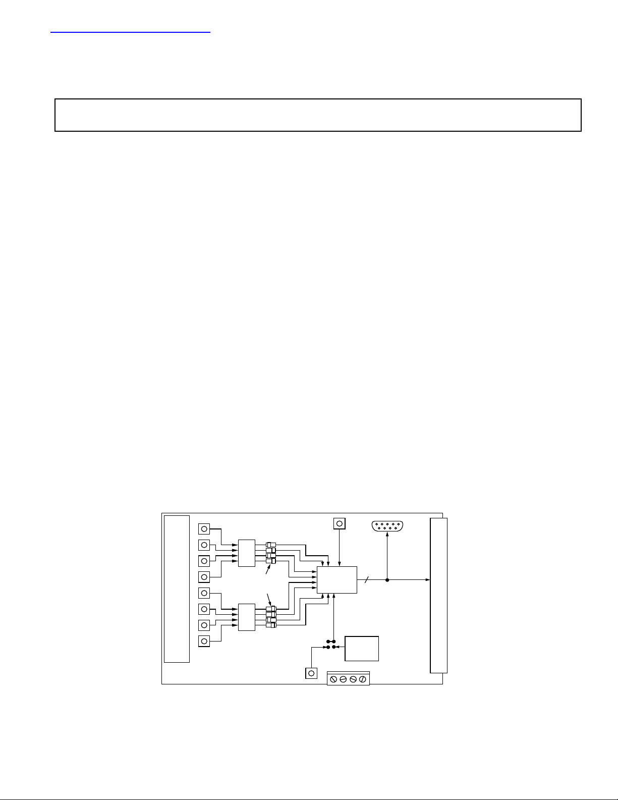
FUNCTIONAL BLOCK DIAGRAM
AIN 8
Prototyping Area
AIN 1
Analog
Inputs
OP467
Range
Selection
Jumpers
OP467
Reference
Input
(+2.5 V)
Conversion
Start Input
REV. A
Information furnished by Analog Devices is believed to be accurate and
reliable. However, no responsibility is assumed by Analog Devices for its
use, nor for any infringements of patents or other rights of third parties
which may result from its use. No license is granted by implication or
otherwise under any patent or patent rights of Analog Devices.
9-Way
D-Type
Connector
96-Way Connecter
Evaluation
AD780
Reference
-12 V
V
DD
12
AD7891-1
Board
DGND
AD7891-1
ADC
+12 V
One Technology Way, P.O. Box 9106, Norwood. MA 02062-9106, U.S.A.
Tel: 617/329-4700 Fax: 617/326-8703
Page 2

EVAL-AD7891-1CB
Link Options
There are thirty one link options on the evaluation board which must be set for the required operating setup before use. The functions of these options are outlined below.
Link No. Function
LK1 - LK8 LK1 to LK8 select the voltages applied to the inputs of the quad op-amp buffers. LK1 selects the voltage for
channel 1, LK2 selects the voltage for channel 2 etc.
In position A, the input is connected to the SMB connector.
In position B, the input is connected to AGND. If no voltage is present at the SMB connector then the link
should be in position B.
LK9 - LK16 LK9 to LK16 are used to select the voltages applied to the V
that is applied to V
, LK10 selects the voltage applied to V
IN1A
In position A the buffered input voltage from AINx is connected to V
In position B, V
is connected to AGND.
INXA
LK17 - LK24 LK17 to LK24 are used to select the voltage applied to the V
voltage that is applied to V
, LK18 selects the voltage that is applied to V
IN1B
In position A, the buffered reference voltage is applied to V
In position B, the buffered input voltage from AINx is connected to V
In position C, V
is connected to AGND.
INXB
LK25 This link option selects the reference source for the AD7891 REF OUT/REF IN pin.
With this link in position A, the reference connects to the SMB socket, SKT9.
In position B, the AD780 +2.5V reference is selected as the reference for the AD7891-1.
With this link out, the REF OUT/REF IN pin remains open-circuited, thus the reference source is the AD7891-1's
internal reference.
LK26 This link selects the V
In position A, the V
In position B, the V
source.
DD
supply is taken from the external VDD connector.
DD
supply is taken from the 96 way connector.
DD
LK27 This link selects the +12V source.
In position A, the +12V supply is taken from the external +12 V connector.
In position B, the +12V supply is taken from the 96 way connector.
LK28 This link selects the -12 V source.
In position A, the -12 V supply is taken from the external -12 V connector.
In position B, the -12 V supply is taken from the 96 way connector.
LK29 This link option selects the voltage applied to the STANDBY pin of the AD7891-1. The voltage applied to the
STANDBY pin can also be controlled from pin 9 of the 9-way D-type socket. If pin 9 of the 9-way D-type socket
is used to control the voltage applied to the STANDBY pin then LK29 should be left unconnected.
In position A, the STANDBY pin is connected to V
DD.
In position B, the STANDBY pin is connected to DGND.
LK30 This link option selects the source for the
In position A, the
CONVST pin is connected to the FL0 pin on the 96-way connector. When using the evaluation
CONVST input of the AD7891-1.
board with the EVAL-CONTROL BOARD, there are two program options, one where the
generated from the EVAL-CONTROL BOARD; the second where the
When the internal
CONVST program is used, this link must be in position A.
In position B, the signal applied to the SMB connector, SKT10 provides the
LK31 This link option selects the voltage applied to the MODE pin of the AD7891-1 and hence selects the interface
mode used for the part.
In position A, the MODE pin is connected to DGND, which selects the serial interface mode.
In position B, the MODE pin is connected to V
, which selects the parallel interface mode.
DD
inputs of the AD7891-1. LK9 selects the voltage
INXA
etc.
IN2A
.
INXA
inputs of the AD7891-1. LK17 selects the
INXB
INXB
.
INXB
etc.
IN2B
.
CONVST signal is
CONVST signal is externally supplied.
CONVST signal for the AD7891-1.
–2–
REV. A
Page 3

EVAL-AD7891-1CB
SET-UP CONDITIONS
Care should be taken before applying power and signals to the
evaluation board to ensure that all link positions are as per the
required operating mode. Table I shows the position in which
all the links are set when the evaluation board is sent out.
Table I. Initial Link and Switch Positions
Link No. Position Function.
LK1 A Input to buffer 1 comes from V
IN1
SMB
connector.
LK2 - LK8 B Inputs to buffers 2 to 8 connected to
AGND.
LK9 - LK16 A V
inputs are connected to relevant
INXA
AINx buffers
LK17 - LK24 C V
LK25 B Connects the AD780's V
inputs are connected to AGND
INXB
pin to the
OUT
AD7891-1's REF OUT/REF IN pin
and thus selects the AD780 as the
reference source for the AD7891-1
LK26 B V
is supplied from the 96-way
DD
connector.
LK27 B +12 V is supplied from the 96-way
connector.
LK28 B -12 V is supplied from the 96-way
connector.
LK29 A
STANDBY pin is connected to V
AD7891-1 does not go into
STANDBY
DD
and
mode.
LK30 B Connects the AD7891-1's
CONVST
pin to the FL0 pin of the edge
connector.
LK31 B MODE pin is connected to VDD and
part is configured for its parallel
operating mode.
EVALUATION BOARD INTERFACING
Interfacing to the evaluation board is either via a 96-way
connector, J1 or a 9-way D-Type connector, J2. J1 is used to
connect the evaluation board to the EVAL-CONTROL
BOARD. It can also be used for parallel interface connections to
the evaluation board when operating the AD7891 in its parallel
interface mode without the EVAL-CONTROL BOARD. J2 is
used for serial interface connections when operating the
AD7891 in its serial interface mode. The pinout for the J1
connector is shown in Figure 1 and its pin designations are
given in Table II. The pinout for the J2 connector is given in
Figure 2 and its corresponding pin designations are given in
Table III.
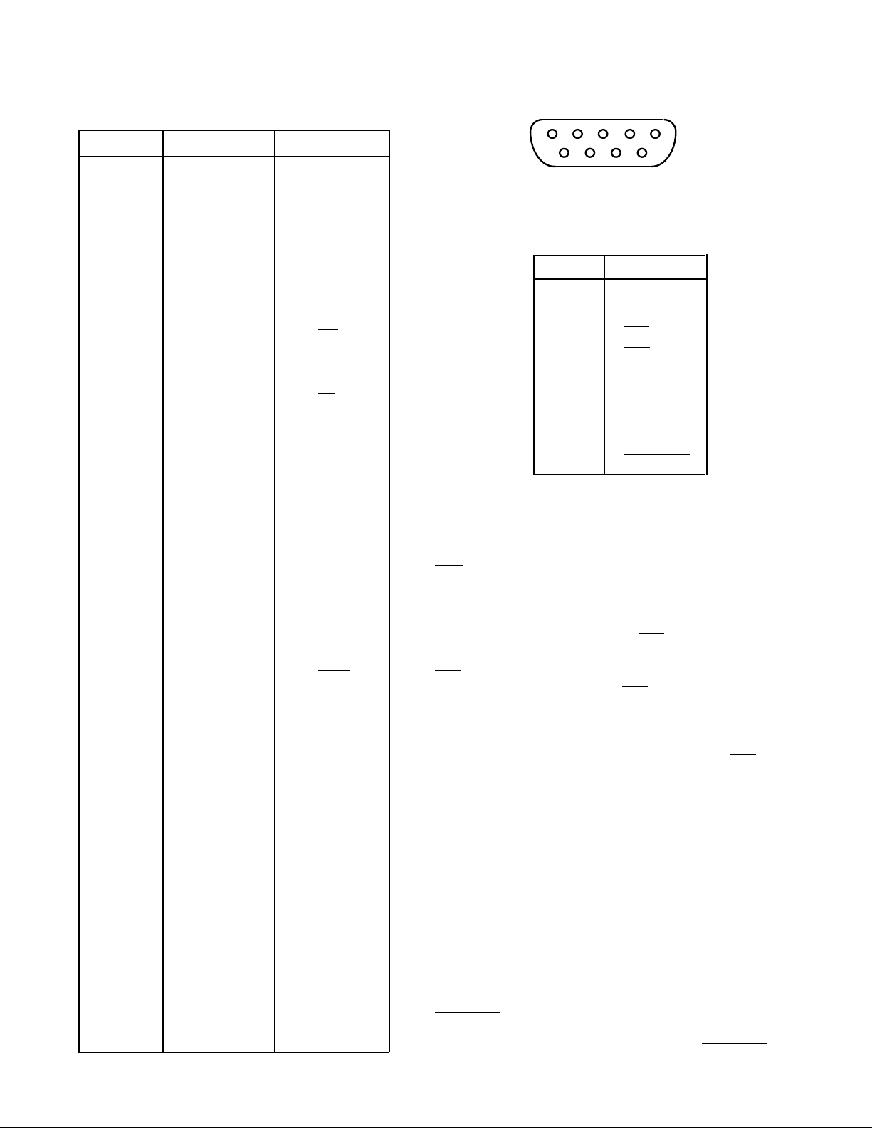
1
A
B
C
1
32
32
Figure 1. Pin Configuration for the 96-Way
Connector, J1
96-Way Connector Pin Description
D0-D11 Data Bit 0 to Data Bit 11. These are three-
state TTL-compatible outputs from the
AD7891-1. Parallel data from the part is
obtained at these pins.
DGND Digital Ground. These lines are connected to
the digital ground plane on the evaluation
board. It allows the user to provide the digital
supply via the connector along with the other
digital signals.
RD Read. This is an active low logic input which
is used in conjunction with
CS low to enable
the data outputs.
CS Chip Select. This is an active low logic input
which is used in conjunction with
enable the data outputs and with
RD low to
WR to allow
input data to be written to the part.
WR Write Input. This is an active low logic input
used in conjunction with
CS to latch the
multiplexer address and software control
information.
FL0 Flag zero. This is a logic input and is con-
nected to the
CONVST logic input on the
device via LK17. A low to high transition on
this input puts the track/hold amplifier into its
hold mode and starts a conversion.
IRQ2 Interrupt Request 2. This is a logic output
and is directly connected to the
EOC logic
output on the device. This active low logic
output indicates the converter status. The end
of conversion is signified by a low-going pulse
on this line.
AGND Analog Ground. These lines are connected to
the analog ground plane on the evaluation
board.
AV
DD
Analog +5V Supply. These lines are connected to the V
supply line on the board.
DD
+12 V +12 V supply used to power op-amps and
voltage reference.
-12 V -12 V supply used to power op-amps.
REV. A
–3–
Page 4
EVAL-AD7891-1CB
Table II. 96-Way Connector Pin Functions.
ROW PIN NO. MNEMONIC
B2D0
B3D1
A 4 DGND
B 4 DGND
C 4 DGND
B5D2
B6D3
B7D4
A9
B9D5
B10D6
C10
B11D7
A 12 DGND
B 12 DGND
C 12 DGND
B13D8
B14D9
B 15 D10
A 16 DGND
B 16 DGND
C 16 DGND
A 17 FL0
B 17 D11
C17
A 20 DGND
B 20 DGND
C 20 DGND
A 22 AGND
A 23 AGND
A 24 AGND
A 25 AGND
A 26 AGND
A 29 AGND
B 29 AGND
C 29 AGND
A31AV
B31AV
C31AV
A32AV
B32AV
C32AV
Note : The remainder of the pins on the 96-way connector are no connects.
RD
CS
IRQ2
SS
SS
SS
DD
DD
DD
1234
678
5
9
Figure 2. Pin Configuration for D-Type Connector, J2
Table III. J2 Pin Functions
PIN NO. MNEMONIC
1 SCLK
2
3
4
EOC
RFS
TFS
5 DATA IN
6 DGND
7 DATA OUT
8V
DD
9 STANDBY
9-Way D-Type Connector Pin Description
SCLK Serial Clock Input. When the device is in its serial
mode, an external serial clock is applied through this
input to obtain serial data from the part.
EOC End-of-Conversion. This output indicates the status of
conversion. A low going pulse on this line signifies the
end of a conversion.
RFS Receive Frame Synchronisation. When the device is in
its serial mode, an external
RFS signal is applied to this
input to obtain serial data from the part.
TFS Transmit Frame Synchronisation. When the part is in
serial mode, an external
TFS signal is applied to this
input when serial data is being written to the part
DATA IN Serial Data Input. Serial data to the part is
applied this input. The serial data should be valid on
the falling edge of SCLK for six edges after
TFS goes
low.
DGND Digital Ground. This line is connected to the digital
ground plane on the evaluation board. It allows the
user to provide the digital supply via the connector
along with the other digital signals.
DATA OUT Serial Data Output. Serial data from the part
is obtained at this output. The serial data is clocked
out by the rising edge of SCLK and is valid on the
falling edge of SCLK for sixteen edges after
RFS goes
low.
DD
+5 V Supply. This line is connected to the VDD supply
V
line on the evaluation board. It allows the user to
provide the digital supply via the connector along with
the other digital signals.
STANDBY Standby Input. When this input is at a logic
zero, the AD7891-1 is put into standby mode. Normal
operation of the part takes place when
STANDBY is
high.
–4–
REV. A
Page 5

EVAL-AD7891-1CB
SOCKETS
There are ten input sockets relevant to the operation of the
AD7891-1 on this evaluation board. The function of these
sockets is outlined in Table IV.
Table IV. Socket Functions
Socket Function
SKT1 - SKT 8 Sub-Minature SMB Socket for A
SKT9 Sub-Minature SMB Socket for external
reference.
SKT10 Sub-Minature SMB Socket for
input.
CONNECTORS
There are two connectors on the AD7891-1 evaluation board as
outlined in Table V.
TABLE V. CONNECTOR FUNCTIONS
Connector Function
J1 96-Way Connector for Parallel Interface connec-
tions.
J2 9-Way D-Type Connector for Serial Interface
connections.
CONVST
IN1 - AIN8
.
OPERATING WITH THE EVAL-CONTROL BOARD
The evaluation board can be operated in a stand-alone mode or
operated in conjunction with the EVAL-CONTROL BOARD.
The EVAL-CONTROL BOARD is available from Analog
Devices under the order entry "EVAL-CONTROL BOARD".
When operated with this control board, all supplies and control
signals for operating the AD7891-1 are provided by the EVALCONTROL BOARD when it is run under control of the
AD7891-1 software which is provided with the AD7891-1
evaluation board package. The EVAL-CONTROL BOARD will
also operate with all Analog Devices evaluation boards which
end with the letters CB in their title.
The 96-way connector on the EVAL-AD7891-1CB plugs
directly into the 96-way connector on the EVAL-CONTROL
BOARD. The EVAL-CONTROL BOARD is powered from a
12V ac transformer. This is a standard 12V ac 1A transformer.
These can also be ordered from Analog Devices under the order
entry "EVAL-110VAC-US' for a 110V compatible transformer
and "EVAL-220VAC-EU" or EVAL-220VAC-UK for a 220V
compatible transformer. These transformers are also available
for other suppliers including Digikey (110V models) and
Campbell Collins (220V models). The EVAL-CONTROL
BOARD generates all the required supplies for itself and the
EVAL-AD7891-1CB.
Connection between the EVAL-CONTROL BOARD and the
serial port of a PC is via a standard RS-232 cable which is
provided as part the EVAL-CONTROL BOARD package.
Please refer to the manual which accompanies the EVALCONTROL BOARD for more details on the EVAL-CONTROL BOARD package.
CONVST for the EVAL-AD7891-1CB can be provided
The
externally or by the EVAL-CONTROL BOARD. The maximum sampling rate of 454 kSps is supported when using either
source for the
CONVST signal.
REV. A
–5–
Page 6

EVAL-AD7891-1CB
Figure 3. Main Screen
SOFTWARE DESCRIPTION
Included in the EVAL-AD7891-1CB evaluation board package
is a PC-compatible disk which contains software for controlling
and evaluating the performance of the AD7891-1 when it is
operated with the EVAL-CONTROL BOARD. The EVALAD7891-1CB Demonstration/Evaluation Software runs under
DOS 4.0 or later and requires a minimum of a 386-based
machine with 400kB of base RAM and 500kB of free hard disk
space. The user interface on the PC is a dedicated program
written especially for the AD7891-1.
The disk which accompanies the EVAL-AD7891-1CB contains
several files. The user should create a new directory on the main
PC drive and label this "AD7891-1". Then, all files on the
EVAL-AD7891-1CB disk should be copied into this directory.
The Mouse Driver on the PC should be enabled before running
the software. If this has not been loaded, the program will not
run.
To run the software, simply make the AD7891-1 directory the
current directory and type "go". When the evaluation program
starts, the user sees the screen shown on Figure 3 (without any
FFT or scope waveforms). This is the main screen and it is
divided into three parts. The top part provides the main control
interface for the AD7891-1 evaluation software. The middle
part of the main screen functions as a Digital Storage
Oscilliscope and the bottom part of the main screen operates as
either a Digital Spectrum Analyzer or a Histogram analyzer.
Each part of the screen has several buttons that can be pressed
by using the mouse or the keyboard. To press a button using
the mouse, simply use it to move the on-screen pointer to the
button to be activated and click. To use the keyboard, simply
press the appropriate key as highlighted on the button. Lower
case letters must be used. When a button is pressed, it is
highlighted on the screen. The next button can be highlighted
by using the Tab key or the previous button by holding down
the shift key and the Tab key together. The highlighted button
can also be pressed by pressing the space bar. Pressing the ESC
key halts any operation currently in progress. In this document, if
a button can be activated from the keyboard then the key used is
shown in bold in the button name. For example, "no prog" has the
"p" highlighted in bold, indicating that the button can be activated by
pressing the p key.
Some buttons have a red indicator. A red indicator on the
button means that the function associated with that button is
on. Absence of the red indicator light means that the function
associated with the button is off. The on/off status of these
buttons is changed simply by selecting the button.
Figure 4. SetupScreen
Setting up the EVAL-CONTROL BOARD
When the software is run, the "F2 Setup" button in the top left
of the screen should be selected to pop up the setup menu.
This menu sets up the EVAL-CONTROL BOARD for use with
the EVAL-AD7891-1CB. The Setup Menu is shown in Figure
4.
Firstly, a configuration file must be chosen. The configuration
file contains the default configuration information for the
EVAL-CONTROL BOARD, the Digital Spectrum Analyzer
and the Digital Storage Oscilliscope. It also tells the AD7891-
1.EXE software which .HIP file to download to the ADSP-
2111. The .HIP file contains the DSP code which is executed
by the ADSP-2111. Normally, the "no prog" button is off, so
when the configuration file is loaded, the .HIP file is automatically downloaded to the ADSP-2111. However, if the "no prog"
button is on, then the .HIP file is not downloaded to the ADSP-
2111.
There are two configuration files for the AD7891-1. If an
external
file "AD7891EX" must be chosen. The mouse or the keyboard
is used to highlight the "AD7891EX" option and the "load
device file" button is pressed. The other configuration file
option is chosen when using the
the EVAL-CONTROL BOARD. The mouse or the keyboard is
used to highlight the "AD7891IN" option and, again, the "load
device file" button is pressed. See Appendix A for further
information about the .CFG files.
After the configuration file is loaded, the sample rate and
number of samples can be changed. If the internal
option is in use, then the available
limited to frequencies of the form 16 MHz/N, where N is an
integer in the range 1 to 65536. If a frequency other than one
of these frequencies is chosen, then the EVAL-CONTROL
BOARD generates the next lowest available frequency.
The input voltage range and the input voltage offset are shown
in the Analog Input "Range" and "Offset". These figures can be
altered if requried. The input voltage range should be set to 10
V for a ±5 V input or to 20 V for a ±10 V input. The offset
voltage should be set to the input voltage which causes the ADC
to return a code of zero. These figures are used for calculating
the Max, Min and PPk (peak to peak) voltage numbers in the
oscilliscope window and also for histogram analyzer
calcualtions.
CONVST pulse is being used, then the configuration
CONVST signal generated by
CONVST
CONVST frequencies are
–6–
REV. A
Page 7

EVAL-AD7891-1CB
Main Screen
The top left part of the main screen contains eight buttons
which are selected using the mouse or by using the function keys
from the keyboard. These buttons and the actions they perform
are:
F1: Info. Activating this button provides information on
the software.
F2: Setup . Pressing this button pops up the Setup Menu.
This menu is described above.
F3: Samp. When this key is pressed, the software causes
the AD7891-1 to perform a number of conversions as
determined by the setup menu (see above). The data
from these conversions is then analyzed by the
AD7891-1 evaluation software. Another set of samples
may be taken by pressing the F3 key again.
F4: Cont. Pressing this button causes the software to
repeatedly perform conversions and analyze them.
Once the conversions and analysis has been done for
one set of samples, the software automatically repeats
the process. It continues to do this until the ESC key
is pressed.
F5: Save. This saves a set of samples to a file for use either
at a later date or with other software. The samples can
be saved either as "volts", "ints" or "binary". The
format of all these files is ASCII text. Note that the
AD7891 software can only load files saved in the "ints"
format. Files saved in the "volts" and "ints" formats can
be used with packages such as Mathcad. Files saved in
the "binary" format are for viewing purposes only.
F6: Load. This allows the user to load data from a file
with a .DAT extension. Only data that was saved as
ints can be loaded and analyzed. A configuration file
must be loaded via the "F2 Setup" menu before the
data file can be analyzed. If there is no EVALCONTROL BOARD connected to the PC, then the
"no prog" button in the "F2 Setup" menu must be on.
Once a configuration file has been loaded, the data
loaded from the .DAT file is analyzed according to the
settings in the "F2 Setup" menu.
F7: Reset. Choosing this option resets the EVAL-
CONTROL BOARD.
F10: Quit. This quits the AD7891-1 evaluation software
and returns control to the operating system.
Information Windows
There are three information windows at the top of the main
screen. The leftmost window is the configuration window and
gives details about part being evaluated. It shows the name of
the program which has been downloaded to the EVAL-CONTROL BOARD, the sampling frequency, the number of bits,
the analog input range of the part and the output code format of
the part. The rightmost large window is the Status window.
This window provides feedback to the user as to what operations are currently being performed by the software and also
displays error messages. Directly underneath the status window
is a small window that shows the maximum and minimum
values of the most recently captured samples.
Test Mode
At the top right of the main screen are the Test Mode buttons.
These buttons determine what sort of testing is done on the
samples captured by the software. Both an ac analysis and dc
analysis can be performed. The function of these buttons are:
fft plot Choosing this button causes the Digital Spectrum
Analyzer to appear at the bottom of the screen.
histogram: Choosing this button causes the Histogram
Analyzer to be displayed at the bottom of the
screen.
There is one other button near the top of the screen, beside the
"F10 Quit" button. This is:
blackman-harris: When performing a fourier transform of the
sampled data, this button determines whether or not
the data is windowed by a blackman-harris window
before the transform. When this button is on, the data
is windowed. When this button is off, the data isn't
windowed. See the Digital Spectrum Analyzer section
for more details.
REV. A
–7–
Page 8

EVAL-AD7891-1CB
Digital Storage Oscilliscope.
When samples of data are captured, they are displayed on the
Digital Storage Oscilliscope. If the blackman-harris button is
turned on then the windowed data is also displayed on the
oscilliscope. The 'scope has been designed to act in a similar
way as a conventional oscilliscope. To the right of the
oscilliscope are several buttons that control the manner in which
data is displayed on the 'scope. The timebase for the
oscilliscope is automatically chosen by the software if the Time/
Div "Auto" button is on. The user can also select the timebase
by clicking in the Time/Div window and scrolling up and down
through the possible timebases. Similarly, the vertical scale of
the oscilliscope is chosen automatically if the Volt/Div "Auto"
button is on. The user also has the option of selecting the
desired vertical scale in a similar manner to selecting the
timebase.
The other buttons associated with the oscilliscope are:
grid This button toggles the grid display of the oscilliscope
on and off.
axis This button toggles the axis display of the oscilliscope
on and off
text This button toggles the text displayed on the
oscilliscope screen on and off.
line When the line button is on, the displayed samples are
joined together by lines. When this button is off, the
samples are displayed as points.
ac When this button is on, the dc component of the
sampled signal is removed and the signal is displayed.
This has the effect of centering the signal vertically on
the oscilliscope screen. When this button is on, the dc
component is not removed and the signal is displayed
with its horizontal axis corresponding to a code of 0.
The ac display option is useful for zooming in on a
low-level signal that has a large dc offset.
dual When the "dual" button is on, the oscilliscope screen is
divided into two parts with the sampled data display
centered on one horizontal axis and the windowed data
display centered on another. When the "dual" button
is off, both traces are centered on the same horizontal
axis.
1 This button toggles the sampled data trace on and off
2 This button toggles the windowed data trace on and
off.
Histogram Analyzer
The histogram analyzer counts the number of occurrences of
each code in the captured samples and displays a histogram of
these counts. The most frequently occurring code is displayed
in the center of the histogram. The analyzer is normally used
with a dc input signal and calculates the mean and the standard
deviation of the sampled data. The mean and standard deviation are displayed in both volts and in units of the lsb size of the
converter. The histogram gives a good indication of the dc
noise performance of the ADC. The standard deviation shows
directly the noise introduced in the conversion process.
–8–
REV. A
Page 9

EVAL-AD7891-1CB
Digital Spectrum Analyzer
The Digital Spectrum Analyzer performs a fast fourier transform
of the sampled data and displays the magnitude of the results on
its screen in decibels (dB). It also calculates the signal to noise
ratio of the sampled data, assuming the samples are those of a
sine wave. If the "blackman-harris" button near the top of the
main screen is on then the data is windowed by a blackmanharris window before the fast fourier transform is performed.
Normally, the "blackman-harris" button needs to be to on in
order to obtain meaningful results from the spectrum analyzer.
If the evaluation board is used in a coherent sampling system,
ie. one where the conversion start signal applied to the AD78911 is synchronized to an input sine wave, in such a way that an
integral number of periods of the sine wave are contained in the
sampled data, then the blackman-harris window can be turned
off.
The buttons to the right of the spectrum analyzer display
control the operation of the analyzer. These buttons are:
Avg When this button is on, the fourier transforms on each
new set of sampled data are averaged so that the noise
floor decreases relative to the signal contained in the
data.
Scale When this button is on, the complete fourier transform
from 0 Hz up to fs/2 is displayed in the spectrum
analyzer window. When this button is off, the first 510
bins (less for transforms of less than 512 points) of the
fourier transform are displayed.
harms When this button is on, the harmonics of the input
signal are included in the SNR calculation. When this
button is off, the harmonics are replaced by average
noise in the SNR calculation.
norm When the "norm" button is on, the fourier transformed
data is normalized so that the zero dB level is set to the
level of the frequency bin with the largest magnitude.
The data is displayed on-screen with the largest
magnitude bin at the zero dB level. When the "norm"
button is off, the data is not normalized. Instead the
zero dB level is assigned to the level that the largest
magnitude input signal would have and the data is
displayed accordingly.
After an FFT has been performed and the frequency spectrum
is displayed in the Digital Spectrum Analyser window, the
mouse may be used to determine the frequency and dB level of
any point in the frequency spectrum. Note that this will only
work when one set of samples were taken, it will not work when
in the continuous sampling mode. Once the mouse is positioned
in the Digital Spectrum Analyser window the cordinates of the
mouse in terms of frequency and dBs will be displayed on the
right hand side of the window.
When a fourier transform of a windowed sine wave is performed, the power contained in the fundamental frequency is
spread out over several frequency bins. To calculate the signal
to noise ratio of the signal, the power contained in those
frequency bins is summed to give the power of the fundamental.
Also, the dc component of the signal is spread over the first few
frequency bins. In the SNR calculation, the dc signal must be
replaced by the average noise.
The number of frequency bins that are summed to give the
power in the fundamental is controlled by the SigBins counter.
The range of valid values is 0 to 9. The number contained in
the SigBins counter is the number of frequency bins each side of
the central peak that are used to calculate the power in the
fundamental frequency. The counter is increased by clicking on
the SigBins "+" button and decreased by pressing on the SigBins
"-" button. As the counter is changed, the SNR is re-calculated
and displayed. For a blackman-harris window, the power in the
central peak plus the power in four bins each side of the central
peak is normally used for SNR calculations. In a coherent
sampled data system, all the power from the sine wave is
contained in one frequency bin. In such a case the SigBins
counter shoud be set to zero.
The number of low frequency bins that are replaced by average
noise in the SNR calculation, is controlled by the DcBins
counter. The range of valid values is 0 to 9. The counter is
increased by clicking on the DcBins "+" button and decreased
by pressing on the DcBins "-" button. As the counter is
changed, the SNR is re-calculated and displayed. For a
blackman-harris window, the first three to five bins are normally
replaced by average noise in the SNR calculation. In a coherent
sampled data system, all the dc power is contained in the first
frequency bin. In such a case the SigBins counter shoud be set
to one.
REV. A
–9–
Page 10

EVAL-AD7891-1CB
APPENDIX A: CONFIGURATION FILE DESCRIPTION
There are two configuration files on the distribution disk that
comes with the AD7891-1 evaluation board. They are
AD7891IN.CFG, which is used when the EVAL-CONTROL
BOARD provides the
which is used when an externally provided
used. They provide initial configuration information to the
AD7891-1.EXE program. Normally no changes need to be
made to the .CFG files. However sometimes it may be desired
to change the initial configuration. This is done by editing the
file to make the changes and then saving the changes before
running the AD7891-1.EXE program. Here is a listing of the
contents of the AD7891IN.CFG file.
[DemoController]
Use69=FALSE
AFlags=TRUE
Sports=FALSE
Voltage=5
[EvalBoard]
Part=AD7891-1
Program=ad7891in.hip
NumBits=12
CONVST signal, and AD7891EX.CFG,
CONVST signal is
MaxFrequency=600000
DefaultFrequency=200000
DefaultNsamp=256
BinaryCoding=TwosComplement
;BinaryCoding=Binary
;BinaryCoding=DffsetBinary
[AnalogInput]
InputRange=10
InputOffset=0
There are three main sections to the configuration file. The
name of each section is given in square brackets in the file
listing. These sections are [DemoController], [EvalBoard] and
[AnalogInput]. Comments are included in the listing by
preceeding the comment with a semi-colon.
[DemoController] section
This section controls some of the settings of the EVALCONTROL BOARD card. These settings should not be
changed.
[EvalBoard] section
This section tells the AD7891-1.EXE program the name of the
part being evaluated, the .HIP program that needs to be
downloaded to the ADSP-2111, the number of bits of the ADC,
the maximum sampling frequency, the default sampling
frequency, the default number of samples to be taken and the
form of coding used by the ADC.
The sampling frequencies are in Hertz. There are three valid
types of binary coding. These are TwosComplement, Binary
and OffsetBinary. Binary and OffsetBinary are interpreted in
the same manner in the AD7891-1.EXE program and may be
used interchangeably.
[AnalogInput] section
InputRange gives the default voltage range of the input channel.
Valid values for InputRange for the AD7891-1 are 10 V (for the
±5 V range) and 20 V (for the ±10 V range). InputOffset is the
input voltage that returns a code of zero from the AD7891-1.
–10–
REV. A
Page 11

COMPONENT LIST
Integrated Circuits
U1-U2 OP467 Quad Op-amp
U3 OP07 Op-Amp
U4 AD7891-1 ADC
U5 AD780 2.5 V Reference
Capacitors
C2-3, C6, C8-10, C12, 10µF Tantalum Capacitor
C16, C18, C23-24, C26
C1, C4-5, C&, C11, C13-15, 0.1µF Ceramic Capacitor
C17, C21-22, C25
C20 10nF Ceramic Capacitor
EVAL-AD7891-1CB
Resistors
R1-10 10kΩ Resistor
Links
LK1-31 Shorting Plug
Sockets
SKT1-10 Sub-Minature BNC Socket
Connectors
J1 9-Way D-Type Connector
J2 96-Way Connector
J3 Power Supply Connector
REV. A
Figure 8. Component placement Map
–11–
Page 12

EVAL-AD7891-1CB
Figure 9. AD7891-1 Evaluation Board Circuit Diagram
–12–
REV. A
 Loading...