

查询EVAL-AD7475供应商查询EVAL-AD7475供应商
a
FEATURES
Full-Featured Evaluation Board for the AD7475/95
EVALUATION-BOARD CONTROLLER Compatible
Stand Alone Capability
On-Board Analog Buffering and Reference
Various Linking Options
PC Software for Control and Data Analysis when used
with EVALUATION-BOARD CONTROLLER
Patchwork Area for User Expansion
INTRODUCTION
This Technical Note describes the evaluation board for
the AD7475/AD7495 which is a fast 12-bit high speed, low
power successive-approximation ADCs. The parts operate
from a sinlge 2.7 V to 5.25 V power supply and feature
throughput rates up to 1 MSPS. Full data on the
AD7475/AD7495 is available in the AD7475/AD7495
data sheet available from Analog Devices and should be
consulted in conjunction with this Technical Note when
using the Evaluation Board.
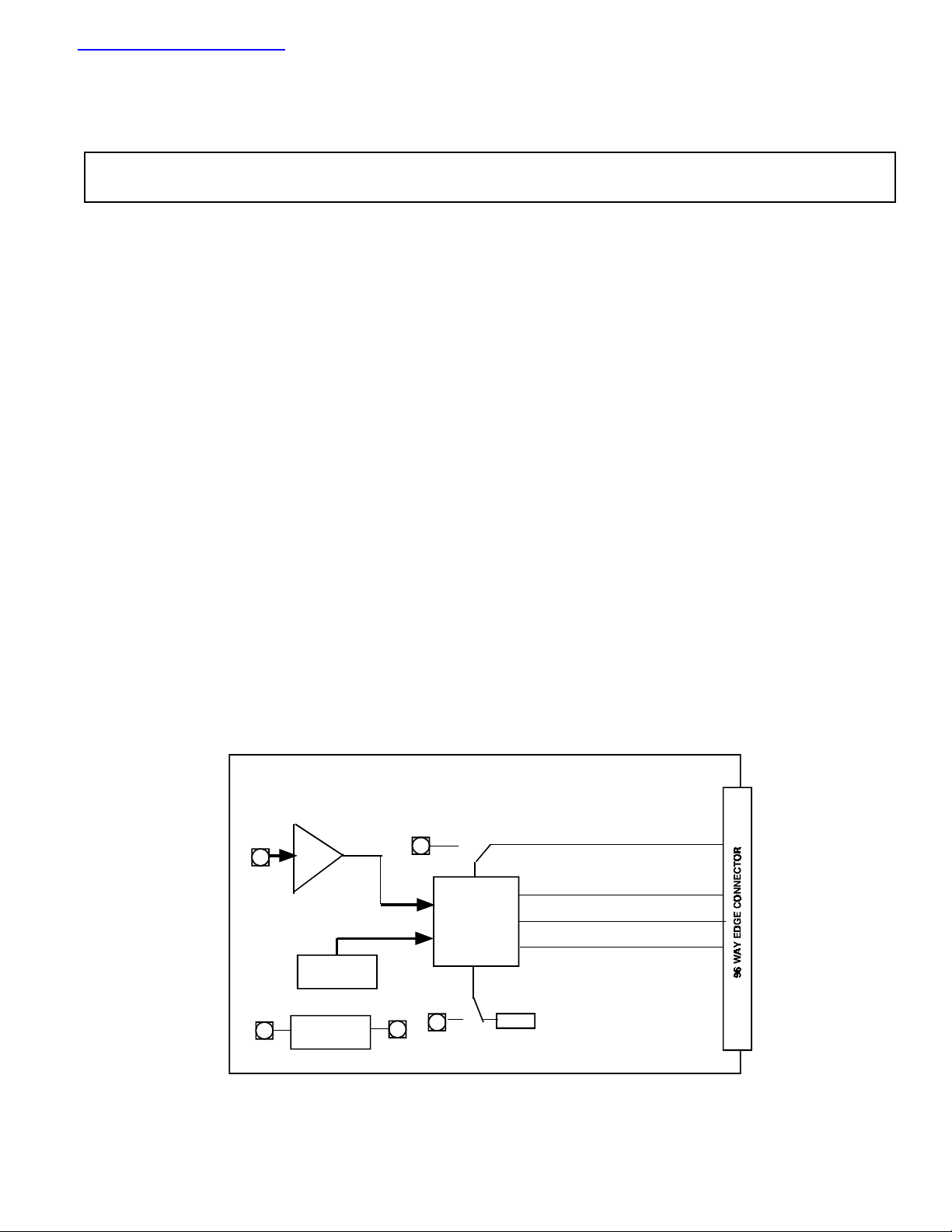
On-board components include an AD780 which is a pin
programmable +2.5V or +3V ultra high precision
bandgap reference and an AD711 op-amp used to buffer
the analog input. There are various link options which are
explained in detail on page 2.
Interfacing to this board is through a 96-way connector.
This 96-way connector is compatible with the EVALUATION-BOARD CONTROLLER which is also available
from Analog Devices. External sockets are provided for
the REFIN input and the VIN input.
FUNCTIONAL BLOCK DIAGRAM
Evaluation Board for 1MSPS, 12-Bit ADC
EVAL-AD7475/AD7495CB
OPERATING THE AD7475/AD7495 EVALUATION
BOARD
Power Supplies
When using this evaluation board with the EVALUATION-BOARD CONTROLLER all supplies are provided from the EVALUATION-BOARD
CONTROLLER through the 96 way connector.
When using the board as a stand alone unit external supplies must be provided. This evaluation board has six
power supply inputs: V
D
. If the evaluation board is used in stand-alone mode
GND
+5V must be connected to the V
AD7475/AD7495 V
ence. +12V and -12V are used to supply the op-amps. The
V
pin can be driven by a voltage between +3V and
DRIVE
+5V allowing the evaluation board to be connected to
both +3V and +5V systems. The supplies are decoupled to
the relevant ground plane with 10µF tantalum and 0.1µF
multilayer ceramic capacitors at the point where they enter
the board. The supply pins of all the op-amps and reference are also decoupled to A
0.1µF ceramic capacitor. The AD7475/AD7495 AV
supply pin is decoupled to A
0.1µF multilayer ceramic capacitors.
Extensive ground planes are used on this board to mini-
mize the effect of high frequency noise interference. There
are two ground planes, A
nected at one location close to the AD7475/AD7495.
, A
DD
pin and the AD780 voltage refer-
DD
GND
, +12V, -12V, A
GND
input to supply the
DD
with 10µF tantalum and a
GND
with 10 µF tantalum and
GND
and D
. These are con-
GND
GND
, and
DD
ANALOG
INPUT
AD7475/A
D7495
EXTERNAL
REFERENCE
BIAS UP CIR-
CUIT
Vdrive
REV. 0
Information furnished by Analog Devices is believed to be accurate and
reliable. However, no responsibility is assumed by Analog Devices for its
use, nor for any infringements of patents or other rights of third parties
which may result from its use. No license is granted by implication or
otherwise under any patent or patent rights of Analog Devices.
Vdd
CS
SDATA
SCLK
Vdd
One Technology Way, P.O. Box 9106, Norwood. MA 02062-9106, U.S.A.
Tel: 617/329-4700 Fax: 617/326-8703

EV AL-AD7475/AD7495CB
LINK AND SWITCH OPTIONS
There are 12 link options which must be set for the required operating setup before using the evaluation board. The
functions of these options are outlined below.
Link No. Function.
LK1 This link is used to connect the input of the AD711 op-amp to ground if the user needs to do this.
When this link is in position "A" a signal applied to the AIN socket is routed to the input of the AD711 opamp. This is the normal application for this link.
When this link is in position "B", the input of the AD711 op-amp is tied to GND.
LK2
LK3 This link is used to select the source of the reference voltage applied to the AD7475 REFIN pin.
LK4 This link selects the source of the V
LK5 This link option selects the source of the VDRIVE input.
LK6 This link option is used to select the source of the +12V supply
LK7 This link option is used to select the source of the -12V supply.
LK8 This link option sets the dc bias voltage applied to the optional bais-up/filter circuit.
LK9 This link option adds a 50 Ohm termination to AGND at the Ain socket. In most applications this link will
LK10 This link option adds a 50 Ohm termination to AGND at the Vin socket. In most applications this link will
LK11, LK12 When both these links are in position "A", for slower SCLK frequencies, giving valid data on the rising edge.
This link option controls the program pin of the AD780 voltage reference.
When this link is "inserted" the AD780 output is set to +3.0 V.
When this link is "removed" the AD780 output is set to +2.5 V
When this link is in position "A", the AD780 provides the 2.5V reference to the AD7475.
When this link is in position "B" an external reference must be supplied to the AD7475 via J5.
For the AD7495 this pin must be removed
+5V supply.
When this link is in position "A" the +5V is supplied from an exteranl source via J6.
When this link is in position "B" the +5V must be supplied from the EVALUATION-BOARD
CONTROLLER
When this link is in position "A" the VDRIVE supply voltage is provided from VDD.
When this link is in position "B" the VDRIVE supply voltage is provided from the EVALUATION-BOARD
CONTROLLER.
When this link is in position "C" an external VDRIVE supply voltage must be supplied via J7.
In position A, the +12V is supplied from the EVALUATION-BOARD CONTROLLER through the 96 way
connector.
In position B, the +12V is supplied from an external source through the power connector, J8.
In position A, the -12V is supplied from the EVALUATION-BOARD CONTROLLER through the 96 way
connector.
In position B, the -12V is supplied from an external source through the power connector, J8.
When the link is in position "A", the bias voltage is set to the same level as the voltage that is applied to the
REF IN on the AD7475 and the REF OUT pin on the AD7495. In this configuration a bipolar anlag input
applied to the Vin SMB socket as a unipolar signal biased around Vref/2. When in position "B", the bias
voltage is set to A
be left unconnected. If a 50 Ohm termination is required, this link should be inserted.
be left unconnected. If a 50 Ohm termination is required, this link should be inserted.
When both these links are in position "B", for fast SCLK frequencies, giving valid data on the falling edge,
the SCLK signal is connected directly to the AD7898 SCLK pin. This is the normal position for these 2 link
options.
. In this configuration the bias up circuit is not used.
GND
DD
–2–
REV. 0

EV AL-AD7475/AD7495CB
SET-UP CONDITIONS
Care should be taken before applying power and signals to the evaluation board to ensure that all link positions are
as per the required operating mode. Table I shows the position in which all the links are set when the evaluation
board is sent out.
Table I. Initial Link and Switch Positions
Link No. Position Function.
LK1 A Ain is tied to the input of the AD711 buffer op-amp.
LK2 removed AD780 is set to provide a + 2.5 V reference.
LK3 A The on-board AD780 voltage reference supplies the REFIN pin of the AD7475.
removed The internal + 2.5V reference on the AD7495 is used on the AD7495 control
board
LK4 B V
LK5 A VDRIVE pin of the AD7475/AD7495 is connected to V
LK6 A +12V supplied from EVAL-CONTROL BOARD via J5.
LK7 A -12V supplied from EVAL-CONTROL BOARD via J5.
LK8 A Vref is chosen as the dc bias voltage for the bias-up circuit.
LK9 removed 50 Ohm termination is not selected.
LK10 removed 50 Ohm termination is not selected.
LK11, LK12 B SCLK signal from EVALUATION-BOARD CONTROLLER is not inverted, (for
(+5V) supplied by the EVALUATION-BOARD CONTROLLER via J5.
DD
(+5V)
DD
faster values of SCLK).
REV. 0
–3–
EV AL-AD7475/AD7495CB
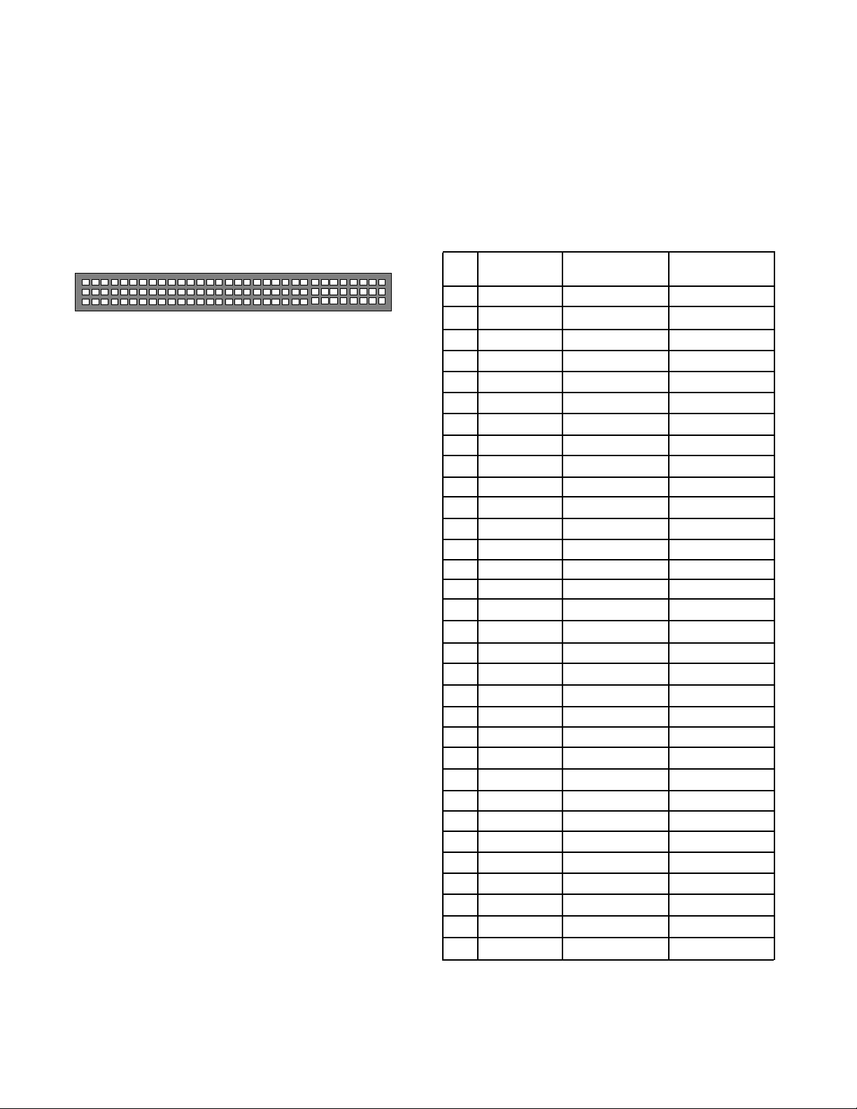
EVALUATION BOARD INTERFACING
Interfacing to the evaluation board is via a 96-way connector, J1. J1 is used to connect the evaluation board to the
EVAL-CONTROL BOARD or other system. The pinout
for the J5 connector is shown in Figure 1 and its pin designations are given in Table II.
1
A
B
C
1
32
32
Figure 1. Pin Configuration for the 96-Way
Connector, J5
96-Way Connector Pin Description
DR0 DATA RECEIVE ONE: Serial Data from the
AD7898 is provided at this output. Sixteen bits of
data are provided with four leading zeroes followed by twelve bits of conversion data which is
provided MSB first.
SCLK0 SERIAL CLOCK ZERO: This continuous clock
is connected to the SCLK pin of the AD7898 via
LK7 to obtain serial data from the AD7898.
TFS0 TRNSMIT FRAME SYNC ZERO,
RFS0 RECEIVE FRAME SYNC ZERO: Both of these
inputs are conncected to the AD7898 CS/
CONVST pin via LK5 to initiate conversions
and to frame the serial data tansfer.
DGND Digital Ground. These lines are connected to
the digital ground plane on the evaluation
board. It allows the user to provide the digital
supply via the connector along with the other
digital signals.
AGND Analog Ground. These lines are connected to
the analog ground plane on the evaluation
board.
AV
DD
Analog +5V Supply. These lines are connected
to the AV
supply line on the board via LK4.
DD
+12V +12V Supply. This line is connected to the +12V
supply line on the board via LK8.
-12V -12V Supply. This line is connected to the -12V
supply line on the board via LK9.
Table II. 96-Way Connector Pin Functions.
ROW A ROWB ROWC
1
2
3
4 DGND DGND DGND
5 DR0
6 TFS0 RFSO
7 SCLK0 SCLK0
8
9
10
11
12 DGND DGND DGND
13
14
15
16 DGND DGND DGND
17
18
19
20 DGND DGND DGND
21 AGND AGND AGND
22 AGND AGND AGND
23 AGND AGND AGND
24 AGND AGND AGND
25 AGND AGND AGND
26 AGND AGND AGND
27 AGND
28 AGND
29 AGND AGND AGND
30 -12V AGND +12V
31
32 AVDD AVDD AVDD
–4–
Note : The unused pins of the 96-way connector are not shown.
REV. 0

EV AL-AD7475/AD7495CB
CONNECTORS
There are nine input/output connectors relevant to the
operation of the AD7475/AD7495 on this evaluation
board. The function of these connectors is outlined in
Table III.
Table III. Connector Functions
Connector Function
J1 Sub-Miniature BNC socket for Ain input.
J2 Sub-Miniature BNC socket for Ext Vref
input.
J3 Sub-Miniature BNC socket for Vin input.
J4 Sub-Miniature BNC socket for Vbiased
output.
J5 96-Way Connector for Serial Interface &
Power Supply connections.
J6 External V
J7 External V
nector.
J8 External +12V, -12V & AGND power con-
nector
& GND power connector.
DD
& GND input power con-
DRIVE
OPERATING WITH THE EVAL-BOARD
CONTROLLER
The evaluation board can be operated in a stand-alone
mode or operated in conjunction with the EVALUATION-BOARD CONTROLLER. This EVALUATIONBOARD CONTROLLER is available from Analog
Devices under the order entry "EVAL-CONTROL
BRD2". When operated with this control board, all supplies and control signals to operate the AD7898 are provided by the EVALUATION-BOARD CONTROLLER
when it is run under control of the AD7475/AD7495 software which is provided with the AD7475/AD7495 evaluation board package . This EVALUATION-BOARD
CONTROLLER will also operate with all Analog Devices evaluation boards which end with the letters CB in
their title.
The 96-way connector on the EVAL-AD7475/AD7495CB
plugs directly into the 96-way connector on the EVALUATION-CONTROL BOARD. No power supplies are required in the system. The EVALUATION-BOARD
CONTROLLER generates all the required supplies for
itself and the EVAL-AD7475/AD7495CB. The EVALUATION-BOARD CONTROLLER is powered from a
12V ac transformer. This is a standard 12V ac transformer
capable of supplying 1A current and is available as an
accessory from Analog Devices under the following part
numbers:
EVAL-110VAC-US: For use in the U.S. or Japan
EVAL-220VAC-UK: For use in the U.K.
EVAL-220VAC-EU: For use in Europe
These transformers are also available for other suppliers
including Digikey (U.S.) and Campbell Collins (U.K.).
Connection between the EVALUATION-BOARD CON-
TROLLER and the serial port of a PC is via a standard
RS-232 cable which is provided as part the EVALUATION-BOARD CONTROLLER package. Please refer to
the manual which accompanies the EVALUATIONBOARD CONTROLER for more details on the EVALUATION-BOARD CONTROLLER package.
REV. 0
–5–

EV AL-AD7475/AD7495CB
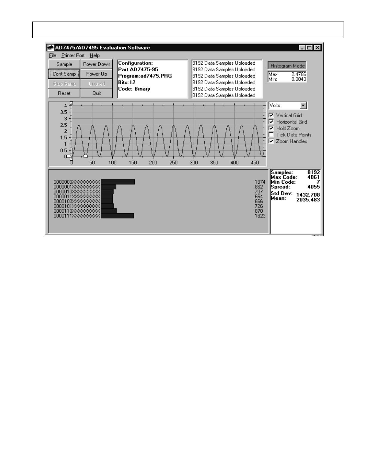
Figure 2. AD7475/AD7495 Main Screen - FFT Mode
SOFTWARE DESCRIPTION
Included in the EVAL-AD7475/AD7495CB evaluation board package is a CD ROM which contains software for controlling
and evaluating the performance of the AD7475/AD7495 when it is operated with the EVALUATION-BOARD CONTROLLER. When the CD is inserted into the PC an installation program will automatically begin. This program will install the
evaluation software onto the users machine and will also install the technical Note for the AD7475/AD7495 evaluation board
as well as the datasheet for the AD7475/AD7495. All literature on the CD is in Adobe's Portable Documation format (PDF)
and will require Acrobat Reader
especially for the AD7475/AD7495.
The software which controls the Evaluation Board Controller and hence the AD7475/AD7495 evaluation board has three main
screens. The screen shown in Figure 2 shows the screen which appears when the software is run. The main function of the
screen is to allow the user to read a predetermined number of samples from the evaluation board and display them in both
the time and frequency domain. The screen can be divided into 3 sections. The upper most section of the screen contains the
control buttons, the menu bar and the status windows.The controll buttons allow the user to enter the set-up menu, take
samples, and get information about the software. There are also power down/up options in the control buttons. These buttons
allow the user to place the part into power down, and power the part up again. There are two powerdown modes associated
with the AD7475/AD7495, partial powerdown and full powerdown. To enter partial power down the ' PowerDown ' button
should be pressed once. To enter Full power down the ' PowerDown ' button should be pressed twice( see modes of operating
section of the AD7475/AD7495 datasheet ).
The menu bar allows the user to select which printer port is to be used to control the Evaluation Board Controller, load and
save data etc. The status window indicates the set up of the AD7475/AD7495 evaluation board, the number of samples taken
and any information messages that are generated.
The middle section of the AD7475/AD7495 Main Screen is a Digital Storage Oscilloscope (DSO). When samples are
uploaded from the Evaluation Board Controller they are displayed here. The samples can be displayed as either interger values
or as voltages . Once the samples are displayed clicking any point on the graph will display the sample number and the value
of the point directly beneath the cursor. Along the axis of the graph are the " zoom handles ". These allow the user to zoom
in and out to get a closer look at a particular sample if required. When another set of samples are taken the graph will attempt
to display all values collected unless the Hold Zoom check box is ticked. If the Hold zoom box is ticked the graph will keep
the same axis settings as for the previous set of data samples. There are additional check boxes in this section to give the user
control over the vertical and horizontal grids and data points.
The lowest section of the screen will show either a Fast Fourier Transform (FFT) of the data, or a histogram, which shows
the number of occurances of each particular code read back. The FFT ( default option ) is typically used when the user is
concerned with examining the AD7475/AD7495's performance in the frequency domain, while the Histogram will give an
indication of the AD7475/AD7495's performance to dc signals. The option displayed can be changed by clicking on the FFT
Mode/Histogram Mode button in the top right of the screen. Figure 3 shows how the Main Screen would look if the Histogram
Mode was selected.
TM
to be viewed or printed. The user interface on the PC is a dedicated program written
–6–
REV. 0
EV AL-AD7475/AD7495CB
Figure 3 AD7898 Main Screen - Histogram Mode
Setup Screen
The Setup Screen is responsible for allowing the user to load
the AD7475/AD7495 configuration file for the evaluation
board. The configuration file will give the software detailed
information about the AD7475/AD7495 evaluation board
and part connected to the Evaluation Board Controller such
as number of bits, maximum sampling rate, power supply
requirements etc. The AD7475/AD7495 configuration file
also tells the software the name of the DSP program file
which it should download to the Evaluation Board Controller. These files are supplied by Analog Devices with the
evaluation board. Figure 4 shows the Setup Screen.
SETTING UP THE EVALUATION BOARD
CONTROLLER
The following text describes how the evaluation board
Evaluation Board Controller and how AD7475/AD7495
software should be set up for the user to begin using the
complete system. The Evaluation Board Controller and
AD7475/AD7495 evaluation board should be connected
together (via the 96 way connector). The power should be
applied to the Evaluation Board Controller. At this stage the
red LED should be flashing which indicates that the Evaluation Board Controller is functional and ready to receive
instructions. The AD7475/AD7495 software which should
have been installed should be loaded before the printer port
cable is connected between the Evaluation Board Controller
and the PC. This will ensure that the printer port has been
initialized properly. The printer port cable can then be
connected between the PC and the Evaluation Board Controller.
Running the AD7475/AD7495 Software
With the hardware setup the user is now in a position to use
the software to control the Evaluation Board Controller and
evaluation board. In the software the user should select the
File menu and click on Setup. This will display the setup
form. A window on the left of the setup form list all the
available configuration files. The configuration files are text
based files which contain information about the particular
evaluation board to be tested - AD7475/AD7495.cfg. The
information will cover such things as the part name, number
of samples to be taken, default and maximum sampling
frequency power supply settings etc. The configuration file
also contains the name of the DSP program file which is to
be downloaded to the Evaluation Board Controller. The user
should select the AD7475.cfg configuration file and click
Load. The AD7475.cfg file will work for both the AD7475
and the AD7495. The Evaluation Board Controller will be
reset and the DSP program will be downloaded. When the
download has been completed the power supply settings
indicated in the configuration file are set and the user may
hear some of the relays clicking. The pull-down menus items
such as number of samples and sampling frequency will have
been set to the default values specified by the configuration
file. The user is free to change these at will. Once all the
settings had been decided the user can click Close to return
to the main form.
REV. 0
–7–

EV AL-AD7475/AD7495CB
Figure 4. The Setup Screen
Taking Samples
When the user clicks Sample the software will instruct the
Evaluation Board Controller to take the required number
of samples at the required frequency from the evaluation
board. These samples are then uploaded and displayed. An
FFT and Histogram are also calculated and displayed. If
the user clicks Cont Samp the software will repeat the
process indefinitely until the user clicks the button again.
While the software is continuously sampling data the other
control buttons are disabled.
Other Buttons
The Reset button will cause the Evaluation Board Controller to perform a reset function. When this happens the
power supplies are turned off and the program in DSP
memory is lost. The user should repeat the setup instructions to download another program if required.
The Quit button will exit the software, the program running on the Evaluation Board Controller is not terminated.
MENU BAR ITEMS
The main screen of the Evaluation Board Controller contains a number of options available as pull-down menu
items. The functions of these are listed below.
File Menu:
Setup Menu: Selecting this option displays the Setup
Screen as shown in Figure 4.
Load Raw Data: Selecting this option allows the user to
load data which had been saved by the software during a
previous session.
Save Raw Data: Selecting this option allows the user to
save the current set of sample data points. The data can be
reloaded to the Evaluation Board Controller software at a
later date or can be used by other programs for further
analysis
Save Binary Data: Selecting this option allows the user to
save the current set of sample data points. The data is
saved in binary format as a text file. This method can be
useful for examining code flicker, looking for stuck bits
etc.
Save FFT Data: Selecting this option allows the user to
save the current set of FFT data points. FFT data cannot
be reloaded into the Evaluation Board Controller software
but can be loaded into other software packages for further
analysis.
Exit: Quits the program.
Printer Port:
This menu item allows the user to select which printer
port should be used for communication with the Evaluation Board Controller.
LPT1: This option selects 0x378 as the printer port
address. This is the default option.
LPT2: This option selects 0x278 as the printer port
address.
PRN: This option selects 0x3BC as the printer port
address.
Help:
This menu item gives information about the current revision of software for the particular evaluation board being
used.
–8–
REV. 0

SOFTWARE CONFIGURATION FILES
Software Configuration Files give the Evaluation Board
Controller software information on how the software and
hardware should perform . They contain information such
as the name of the DSP program to download, the default
and maximum sample frequencies, the number of samples
to take and the power supply settings to use. A typical
Software Configuration File (*.cfg) is shown in Listing 1.
[EVAL-CONTROL BOARD]
partname:AD7475
programname:ad7475.PRG
samplefrequency:100000
maxsamplefrequency:1000000
samples:2048
+/-15V:on
dvdd:5:on
avdd:5:on
bus:on
;options 2scomp, binary
dataformat:binary
numberofbits:12
inputVmax:2.5
inputVmin:0
EV AL-AD7475/AD7495CB
REV. 0
–9–

EV AL-AD7475/AD7495CB
Figure 4. AD7475/95 Evaluation Board Circuit Diagram
–10–
REV. 0

EV AL-AD7475/AD7495CB
Qty Reference Designator Description/Value Manuf. No. Supplier No.
14 C1 C4 C5 C10 C11 C13 C16 C19 10uF 35V Tant. TAP10K35CCSY FEC 664-881
C21 C23 C25 C26 C28 C33
15 C2 C3 C6 C9 C12 C14 C15 C17 0.1uF Ceramic 50 V MCDR25104X7RK0050 FEC 750-920
C18 C20 C22 C24 C27 C29 C32
1 C7 0.01uF Ceramic 50 V MCDR25103X7RK0050 FEC 750-890
1 C8 0.22uF Ceramic 50 V MCDR50224X7RK0050 FEC 750-967
1 C8 0.1uF Ceramic 50 V MCDR50104X7RK0050 FEC 750-955
2 C30 C31 68pF Ceramic MR051A680JT0001 FEC 669-714
5 R1 R2 R3 R4 R6 1K 0.25W 0.1% RC55 Welwyn FEC 339-179
1 R5 3K 0.25W 0.1% RC55 Welwyn FEC 339-635
2 R7 R8 51W 0.25W 1% Multicomp FEC 543-070
1 D1 SD103C Schottky Diode DO35
1 U1 AD711KN Op-Amp ADI AD711KN ADI
1 U2 AD780AN Voltage Reference ADI AD780AN ADI
1 U3 ADOP467G ADI ADOP467G ADI
1 U4 AD7495AR SO8NB ADI
1 U5 74LS04N DM74LS04N FEC 373-450
3 J1 J2 J3 J4 50W Gold Plated PCB SMB Jack M/ACOM FEC 310-682
1 J5 DIN41612 C96 900 plug Siemens FEC 104-986
2 J6 J7 2 Pin Power Connector Lumberg KRM2 FEC 151-785
1 J8 3 PIN Power Connector Lumberg KRM3 FEC 151-786
8 LK1 LK3 LK4 LK6-LK8 LK11 LK12 2x2 Way Jumper Harwin FEC 511-791
3 LK2 LK9 LK10 2 Way Jumper Harwin FEC 511-705
1 LK5 2x3 way jumper Harwin FEC 511-780
3 T1 T2 T3 Black Testpoint W Huges FEC 240-333
2 U1 U2 U3 U5 Ultra low profile socket strip Harwin FEC 519-959
4 Each corner Stick on feet 3M FEC 651-813
1 EVAL-AD7495CB P.C.B.
Figure 4. AD7475/95CB Bill of Materials
REV. 0
–11–

EV AL-AD7475/AD7495CB
Figure 5. Component Side Artwork
Figure 6. Solder Side Artwork
–12–
REV. 0

EV AL-AD7475/AD7495CB
Figure 7. AD7475/AD7495 Evaluation Board Component Placement Drawing.
REV. 0
–13–
 Loading...