

Multichannel,
a
FEATURES
5 V Stereo Audio System with 3.3 V Tolerant Digital
Interface
Supports 96 kHz Sample Rates on Six Channels and
192 kHz on 2 Channels
Supports 16-/20-/24-Bit Word Lengths
Multibit Sigma-Delta Modulators with
“Perfect Differential Linearity Restoration” for
Reduced Idle Tones and Noise Floor
Data Directed Scrambling DACs—Least Sensitive to
Jitter
Differential Output for Optimum Performance
DACs Signal-to-Noise and Dynamic Range: 110 dB
–94 dB THD + N—6-Channel Mode
–95 dB THD + N—2-Channel Mode
On-Chip Volume Control Per Channel with 1024-Step
Linear Scale
Software Controllable Clickless Mute
Digital De-Emphasis Processing
Supports 256 ⴛ f
Clock Modes
Power-Down Mode Plus Soft Power-Down Mode
Flexible Serial Data Port with Right-Justified, Left-
Justified, I2S-Compatible and DSP Serial Port Modes
Supports Packed Data Mode (TDM) for DACs
48-Lead LQFP Plastic Package
APPLICATIONS
DVD Video and Audio Players
Home Theatre Systems
Automotive Audio Systems
Set-Top Boxes
Digital Audio Effects Processors
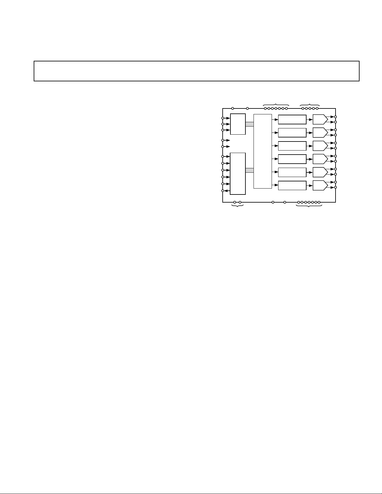
GENERAL DESCRIPTION
The AD1833 is a complete, high-performance, single-chip, multichannel, digital audio playback system. It features six audio
playback channels each comprising a high-performance digital
interpolation filter, a multibit sigma-delta modulator featuring
Analog Devices patented technology and a continuous-time
voltage-out analog DAC section. Other features include an on-chip
clickless attenuator and mute capability, per channel, programmed
through an SPI-compatible serial control port.
, 512ⴛ fS, and 768ⴛ fS Master
S
24-Bit, 192 kHz, ⌺-⌬ DAC
AD1833
FUNCTIONAL BLOCK DIAGRAM
ZERO FLAGS
FILTER
ENGINE
AD1833
INTERPOLATOR
INTERPOLATOR
INTERPOLATOR
INTERPOLATOR
INTERPOLATOR
INTERPOLATOR
FILTR FILTD
CDATA
CLATCH
CCLK
MCLK
RESET
L/RCLK
BCLK
SDIN1
SDIN2
SDIN3
SOUT
DVDD1 DVDD2
SPI
PORT
DATA
PORT
DGND
The AD1833 is fully compatible with all known DVD formats,
catering for up to 24-bit word lengths at sample rates of 48 kHz
and 96 kHz on all six channels while supporting a 192 kHz
sample rate on two channels. It also provides the “Redbook”
standard 50 µs/15 µs digital de-emphasis filters at sample rates
of 32 kHz, 44.1 kHz, and 48 kHz.
The AD1833 has a very flexible serial data input port that allows
for glueless interconnection to a variety of ADCs, DSP chips,
AES/EBU receivers, and sample rate converters. The AD1833
can be configured in left-justified, I
serial port compatible modes. The AD1833 accepts serial audio
data in MSB first, two’s complement format. While the AD1833
can be operated from a single 5 V power supply, it also features
a separate supply pin for its digital interface which allows the
device to be interfaced to devices using 3.3 V power supplies.
It is fabricated on a single monolithic integrated circuit and is
housed in a 48-lead LQFP package for operation over the temperature range –40°C to +85°C.
AVDD
DAC
DAC
DAC
DAC
DAC
DAC
AGND
2
S, right-justified, or DSP
OUTLP1
OUTLN1
OUTLP2
OUTLN2
OUTLP3
OUTLN3
OUTRP3
OUTRN3
OUTRP2
OUTRN2
OUTRP1
OUTRN1
REV. 0
Information furnished by Analog Devices is believed to be accurate and
reliable. However, no responsibility is assumed by Analog Devices for its
use, nor for any infringements of patents or other rights of third parties that
may result from its use. No license is granted by implication or otherwise
under any patent or patent rights of Analog Devices.
One Technology Way, P.O. Box 9106, Norwood, MA 02062-9106, U.S.A.
Tel: 781/329-4700 www.analog.com
Fax: 781/326-8703 © Analog Devices, Inc., 2001

AD1833–SPECIFICATIONS
TEST CONDITIONS UNLESS OTHERWISE NOTED
Supply Voltages (AVDD, DVDD) 5.0 V
Ambient Temperature 25°C
Input Clock 12.288 MHz, (256 × f
Input Signal Nominally 1 kHz, 0 dBFS (Full Scale)
Input Sample Rate 48 kHz
Measurement Bandwidth 20 Hz to 20 kHz
Word Width 24 Bits
Load Capacitance 500 pF
Load Impedance 10 kΩ
NOTES
Performance of all channels are identical (exclusive of the Interchannel Gain Mismatch and Interchannel Phase Deviation specifications).
Specifications subject to change without notice.
Parameter Min Typ Max Unit Test Conditions
ANALOG PERFORMANCE
DIGITAL-TO-ANALOG CONVERTERS
Dynamic Range (20 Hz to 20 kHz, –60 dBFS Input)
With A-Weighted Filter 106.5 110 dB
Total Harmonic Distortion + Noise –95 –89 dB Two Channels Active
SNR 110 dB
Interchannel Isolation 108 dB
DC Accuracy
Gain Error ± 3.0 %
Interchannel Gain Mismatch 0.2 %
Gain Drift 80 ppm/°C
Interchannel Crosstalk (EIAJ Method) –120 dB
Interchannel Phase Deviation ± 0.1 Degrees
Volume Control Step Size (1023 Linear Steps) 0.098 %
Volume Control Range (Max Attenuation) 63.5 dB
Mute Attenuation –120 dB
De-Emphasis Gain Error ± 0.1 dB
Full-Scale Output Voltage at Each Pin (Single-Ended) 1.0 (2.8) V rms (V p-p)
Output Resistance Measured Differentially 150 Ω
Common-Mode Output Volts 2.2 V
DAC INTERPOLATION FILTER—48 kHz
Pass Band 20 kHz
Pass Band Ripple ± 0.01 dB
Stop Band 24 kHz
Stop Band Attenuation 70 dB
Group Delay 510 µs
DAC INTERPOLATION FILTER—96 kHz
Pass Band 37.7 kHz
Pass Band Ripple ± 0.03 dB
Stop Band 55.034 kHz
Stop Band Attenuation 70 dB
Group Delay 160 µs
DAC INTERPOLATION FILTER—192 kHz
Pass Band 89.954 kHz
Pass Band Ripple ± 1dB
Stop Band 104.85 kHz
Stop Band Attenuation 70 dB
Group Delay 140 µs
Mode)
S
110.5 dB f
–94 dB Six Channels Active
–95 dB 96 kHz, Two Channels Active
–94 dB 96 kHz, Six Channels Active
= 96 kHz
S
–2–
REV. 0
AD1833
WARNING!
ESD SENSITIVE DEVICE
Parameter Min Typ Max Unit Test Conditions
DIGITAL I/O
Input Voltage HI 3.0 V
Input Voltage LO 0.8 V
Output Voltage HI DV
Output Voltage LO 0.4 V
POWER SUPPLIES
Supply Voltage (AV
Supply Voltage (DV
Supply Current I
Supply Current I
and DV
DD
) 3.3 DV
DD2
ANALOG
DIGITAL
) 4.5 5.0 5.5 V
DD1
Power Supply Rejection Ratio
1 kHz 300 mV p-p Signal at Analog Supply Pins –60 dB
20 kHz 300 mV p-p Signal at Analog Supply Pins –50 dB
Specifications subject to change without notice.
– 0.4 V
DD2
38.5 42 mA
42 45.5 mA Active
2 mA Power-Down
DD1
V
ABSOLUTE MAXIMUM RATINGS*
(TA = 25°C unless otherwise noted)
AVDD, DV
to AGND, DGND . . . . . . . . –0.3 V to +6.5 V
DDx
AGND to DGND . . . . . . . . . . . . . . . . . . . . –0.3 V to +0.3 V
Digital I/O Voltage to DGND . . . . . –0.3 V to DV
Analog I/O Voltage to AGND . . . . . . –0.3 V to AV
+ 0.3 V
DD2
+ 0.3 V
DD
Operating Temperature Range
Industrial (A Version) . . . . . . . . . . . . . . . –40°C to +85°C
Storage Temperature Range . . . . . . . . . . . . –65°C to +150°C
LQFP, θJA Thermal Impedance . . . . . . . . . . . . . . . . . 91°C/W
Lead Temperature, Soldering
Vapor Phase (60 sec) . . . . . . . . . . . . . . . . . . . . . . . . 215°C
Infrared (15 sec) . . . . . . . . . . . . . . . . . . . . . . . . . . . . 220°C
*Stresses above those listed under Absolute Maximum Ratings may cause perma-
nent damage to the device. This is a stress rating only; functional operation of the
device at these or any other conditions above those listed in the operational
sections of this specification is not implied. Exposure to absolute maximum rating
conditions for extended periods may affect device reliability. Only one absolute
maximum rating may be applied at any one time.
Maximum Junction Temperature . . . . . . . . . . . . . . . . 150°C
ORDERING GUIDE
Model Temperature Range Package Description Package Option
AD1833AST –40°C to +85°C Thin Plastic Quad Flatpack ST-48
EVAL-AD1833EB Evaluation Board
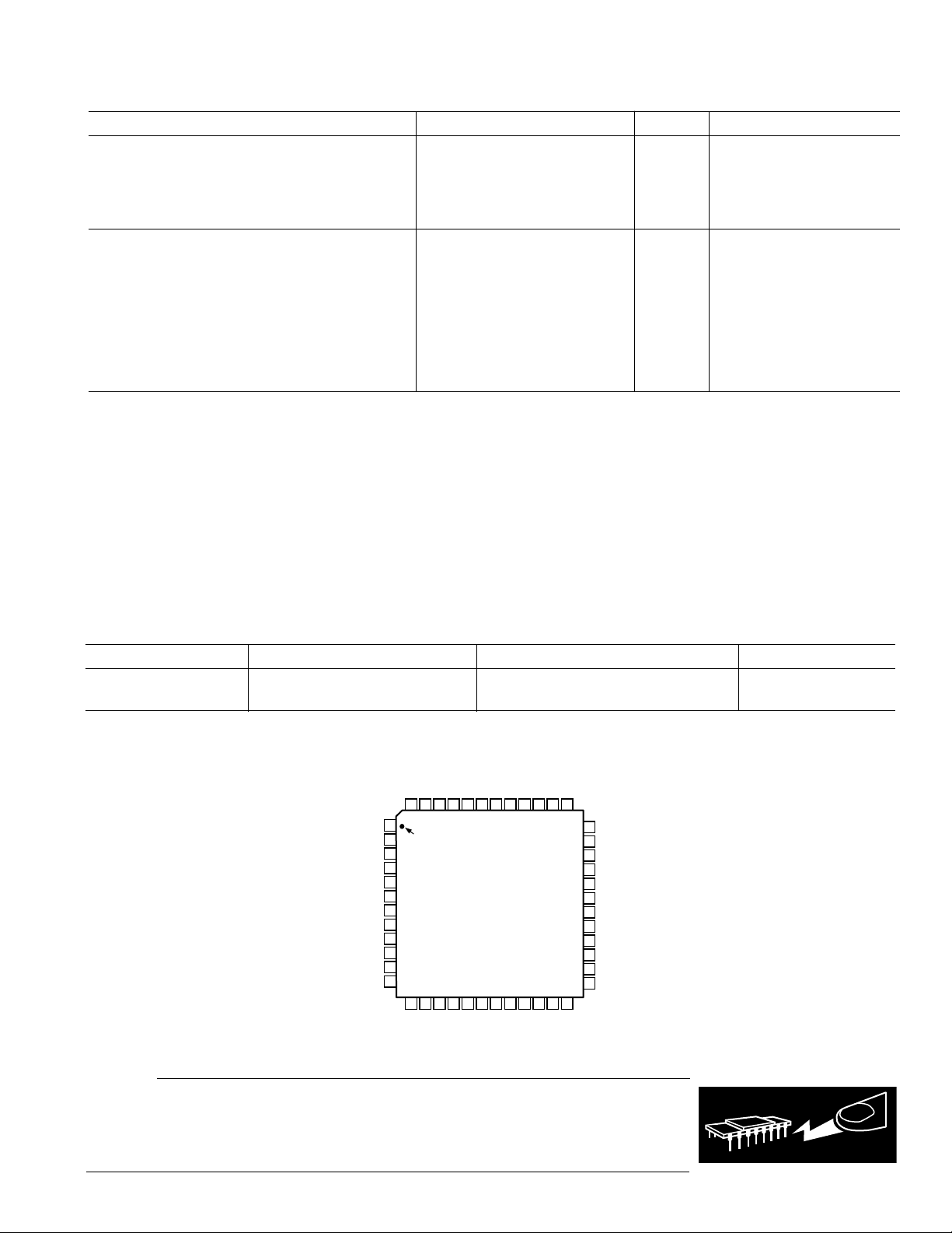
PIN CONFIGURATION
OUTLN2
OUTLP2
OUTLN3
OUTLP3
AVDD
FILTD
FILTR
AGND
OUTRP3
OUTRN3
OUTRP2
OUTRN2
36
35
34
33
32
31
30
29
28
27
26
25
OUTRP1
OUTRN1
AVDD
AVDD
AGND
AGND
AGND
DGND
DVDD2
RESET
ZERO1L
ZERO1R
OUTLP1
OUTLN1
AVDD
AVDD
AGND
AGND
AGND
DGND
DVDD1
ZEROA
ZERO3R
ZERO3L
48 47 46 45 44 39 38 3743 42 41 40
1
PIN 1
2
IDENTIFIER
3
4
5
6
7
8
9
10
11
12
13 14 15 16 17 18 19 20 21 22 23 24
AD1833
TOP VIEW
(Not to Scale)
CCLK
ZERO2R
CLATCH
CDATA
L/RCLK
BCLK
MCLK
SDIN1
SDIN2
SDIN3
SOUT
ZERO2L
CAUTION
ESD (electrostatic discharge) sensitive device. Electrostatic charges as high as 4000 V readily
accumulate on the human body and test equipment and can discharge without detection. Although
the AD1833 features proprietary ESD protection circuitry, permanent damage may occur on
devices subjected to high-energy electrostatic discharges. Therefore, proper ESD precautions are
recommended to avoid performance degradation or loss of functionality.
REV. 0
–3–
AD1833
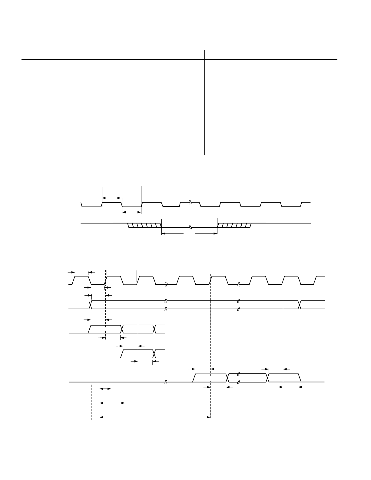
DIGITAL TIMING (Guaranteed over –40ⴗC to +85ⴗC, AVDD = DVDD = 5.0 V ⴞ 10%)
t
DML
t
DMH
t
DBH
t
DBL
t
DLS
t
DLH
t
DDS
t
DDH
t
PDRP
t
CCH
t
CCL
t
CSU
t
CHD
t
CLH
Specifications subject to change without notice.
MCLK LO Pulsewidth (All Modes) 15 ns
MCLK HI Pulsewidth (All Modes) 15 ns
BCLK HI Pulsewidth 15 ns
BCLK LO Pulsewidth 15 ns
LRCLK Setup 5 ns
LRCLK Hold (DSP Serial Port Mode Only) 10 ns
SDATA Setup 5 ns
SDATA Hold 15 ns
PD/RST LO Pulsewidth 10 ns
CCLK HI Pulsewidth 10 ns
CCLK LO Pulsewidth 10 ns
CDATA Setup Time 5 ns
CDATA Hold Time 10 ns
CLATCH HI Pulsewidth 10 ns
t
DMH
MCLK INPUT
Min Unit
RESET INPUT
BCLK
L/RCLK
SDATA
LEFT-JUSTIFIED
MODE
SDATA
2
I
S-JUSTIFIED
MODE
RIGHT-JUSTIFIED
SDATA
MODE
t
DML
t
PDRP
Figure 1. MCLK and
t
DBH
t
DBL
t
DLS
t
DDS
MSB
t
DDH
8-BIT CLOCKS
(24-BIT DATA)
12-BIT CLOCKS
(20-BIT DATA)
16-BIT CLOCKS
(16-BIT DATA)
t
DDS
MSB-1
MSB
t
DDH
RESET
t
DDS
Timing
MSB
t
DDH
t
DDS
LSB
t
DDH
Figure 2. Serial Data Port Timing
–4–
REV. 0
AD1833
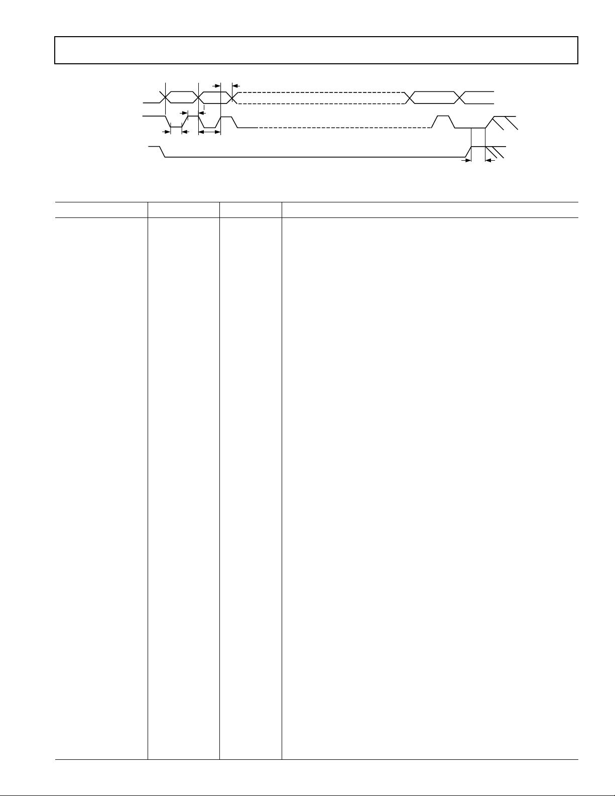
t
CHD
CDATA
CCLK
CLATCH
Pin Mnemonic IN/OUT Description
1 OUTLP1 O DAC 1 Left Channel Positive Output.
2 OUTLN1 O DAC 1 Left Channel Negative Output.
3, 4, 33, 34, 44 AVDD Analog Supply.
5, 6, 7, 30, 31, 32, 41 AGND Analog Ground.
8, 29 DGND Digital Ground.
9 DVDD1 Digital Supply to Core Logic.
10 ZEROA O Flag to Indicate Zero Input on All Channels.
11 ZERO3R O Flag to Indicate Zero Input on Channel 3 Right.
12 ZERO3L O Flag to Indicate Zero Input on Channel 3 Left.
13 ZERO2R O Flag to Indicate Zero Input on Channel 2 Right.
14 CLATCH I Latch Input for Control Data (SPI Port).
15 CDATA I Serial Control Data Input (SPI Port).
16 CCLK I Clock Input for Control Data (SPI Port).
17 L/RCLK I/O Left/Right Clock for DAC Data Input (FSTDM Output in TDM Mode).
18 BCLK I/O Bit Clock for DAC Data Input (BCLKTDM Output in TDM Mode).
19 MCLK I Master Clock Input.
20 SDIN1 I Data Input for Channel 1 Left/Right (Data Stream Input in TDM
21 SDIN2 I/O Data Input for Channel 2 Left/Right (L/RCLK Output to Auxiliary
22 SDIN3 I/O Data Input for Channel 3 Left/Right (BCLK Output to Auxiliary
23 SOUT O Auxiliary I
24 ZERO2L O Flag to Indicate Zero Input on Channel 2 Left.
25 ZERO1R O Flag to Indicate Zero Input on Channel 1 Right.
26 ZERO1L O Flag to Indicate Zero Input on Channel 1 Left.
27 RESET I Power-Down and Reset Control.
28 DVDD2 Power Supply to External Interface Logic.
35 OUTRN1 O DAC 1 Right Channel Negative Output.
36 OUTRP1 O DAC 1 Right Channel Positive Output.
37 OUTRN2 O DAC 2 Right Channel Negative Output.
38 OUTRP2 O DAC 2 Right Channel Positive Output.
39 OUTRN3 O DAC 3 Right Channel Negative Output.
40 OUTRP3 O DAC 3 Right Channel Positive Output.
42 FILTR Reference/Filter Capacitor Connection. Recommend 10 µF/100 µF
43 FILTD Filter Capacitor Connection. Recommend 10 µF/100 µF Decouple to
45 OUTLP3 O DAC 3 Left Channel Positive Output.
46 OUTLN3 O DAC 3 Left Channel Negative Output.
47 OUTLP2 O DAC 2 Left Channel Positive Output.
48 OUTLN2 O DAC 2 Left Channel Negative Output.
D15
t
CCH
t
CCL
D14
t
CSU
D0
t
CLH
Figure 3. SPI Timing
PIN FUNCTION DESCRIPTIONS
and Packed Modes).
DAC in TDM Mode).
DAC in TDM Mode).
2
S Output (Available in TDM Mode).
Decouple to Analog Ground.
Analog Ground.
REV. 0
–5–
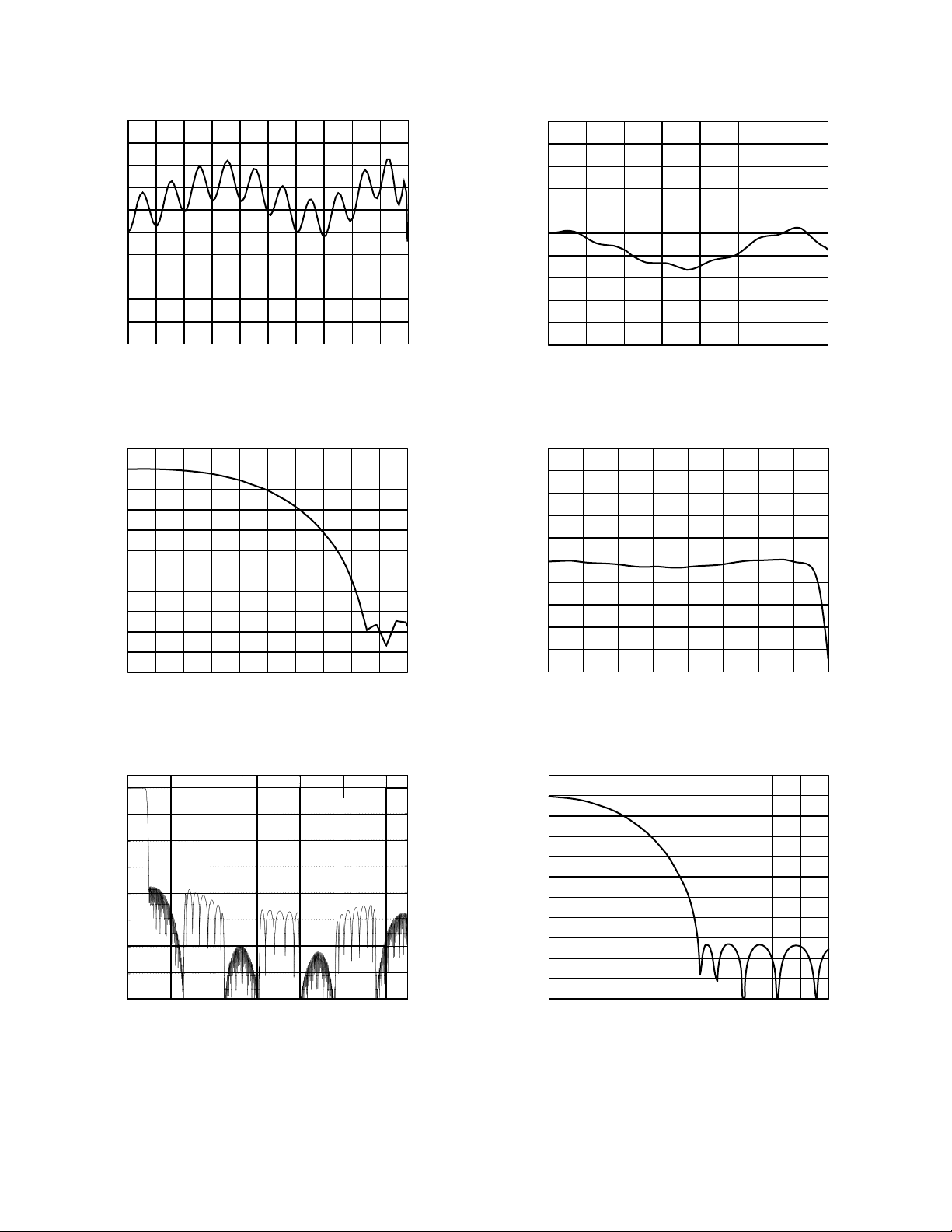
AD1833–Typical Performance Characteristics
0.01
0.008
0.006
0.004
0.002
0
dB
–0.002
–0.004
–0.006
–0.008
–0.01
0 0.2 0.4 0.6 0.8 1.0 1.2 1.4 1.6 1.8 2.0
Hz ⴛ10
TPC 1. Pass Band Response, 8× Mode
10
0
–10
–20
–30
–40
dB
–50
–60
–70
–80
–90
–100
2.00 2.05 2.10 2.15 2.20 2.25 2.30 2.35 2.40 2.45 2.50
Hz ⴛ10
TPC 2. Transition Band Response, 8× Mode
0.1
0.08
0.06
0.04
0.02
0
dB
–0.02
–0.04
–0.06
–0.08
–0.1
4
0 0.5 1.0 1.5 2.0 2.5 3.0 3.5
Hz ⴛ10
4
TPC 4. Pass Band Response, 4× Mode
0.5
0.4
0.3
0.2
0.1
0
dB
–0.1
–0.2
–0.3
–0.4
–0.5
4
0 0.5 1.0 1.5 2.0 2.5 3.0 3.5 4.0
Hz ⴛ10
4
TPC 5. 40 kHz Pass Band Response, 4× Mode
0
–20
–40
–60
dB
–80
–100
–120
–140
–160
0 0.5 1.5 2.0 2.5 3.0
1.0
Hz ⴛ10
TPC 3. Complete Response, 8× Mode
10
0
–10
–20
–30
–40
dB
–50
–60
–70
–80
–90
–100
5
4.0 4.2 4.4 4.6 4.8 5.0 5.2 5.4 5.6 5.8 6.0
Hz ⴛ10
4
TPC 6. Transition Band Response, 4× Mode
–6–
REV. 0

0
10
0.80 0.85 0.90 0.95 1.00 1.05 1.10 1.15 1.20
0
–10
–20
–30
dB
Hz ⴛ10
5
–40
–50
–60
–70
–80
–90
–100
0 0.5 1.5 2.0
0
–20
–40
–60
–80
–100
–120
–140
–160
dB
Hz ⴛ10
5
1.0
–20
–40
–60
dB
–80
–100
–120
–140
–160
0 0.5 1.5 2.0
1.0 2.5 3.0
Hz ⴛ10
TPC 7. Complete Response, 4× Mode
2.0
1.5
1.0
0.5
AD1833
5
TPC 9. Transition Band Response, 2× Mode
0
dB
–0.5
–1.0
–1.5
–2.0
012345678
TPC 8. 80 kHz Pass Band Response, 2× Mode
REV. 0
Hz ⴛ10
4
TPC 10. Complete Response, 2× Mode
–7–

AD1833
FUNCTIONAL DESCRIPTION
Device Architecture
The AD1833 is a 6-channel audio DAC featuring multibit
Sigma-Delta (Σ-∆) technology. The AD1833 features three
stereo converters (giving six channels) where each stereo channel
is controlled by a common bit-clock (BCLK) and synchronization signal (L/RCLK).
Interpolator
The interpolator consists of up to three stages of sample rate
doubling and half-band filtering followed by a 16 sample zero
order hold. The sample rate doubling is achieved by zero stuffing the input samples, and a digital half band filter is then used
to remove any images above the band of interest and to bring
the zero samples to their correct values.
By selecting different input sample rates, one, two, or all three
stages of doubling may be switched in. This allows for three
different sample rate inputs. All three doubling stages are used
with the 48 kHz input sample rate, with the 96 kHz input sample
rate only two doubling stages are used, and with the 192 kHz
input sample rate only one doubling stage is used. In each case
the input sample frequency is increased to 384 kHz. The ZeroOrder Hold (ZOH) holds the interpolator samples for upsampling
by the modulator. This is done at a rate 16 times the interpolator output sample rate.
Modulator
The modulator is a 6-bit, second-order implementation and
uses data scrambling techniques to achieve perfect linearity.
The modulator samples the output of the interpolator stage(s) at
a rate of 6.144 MHz.
OPERATING FEATURES
SPI Register Definitions
The SPI port allows flexible control of the devices’ programmable functions. It is organized around nine registers; six
individual channel VOLUME registers and three CONTROL
registers. Each WRITE operation to the AD1833 SPI control
port requires 16 bits of serial data in MSB-first format. The four
most significant bits are used to select one of nine registers (seven
register addresses are reserved), and the bottom 10 bits are then
written to that register. This allows a write to one of the nine
registers in a single 16-bit transaction. The SPI CCLK signal is
used to clock in the data. The incoming data should change on
the falling edge of this signal and remain valid during the rising
edge. At the end of the 16 CCLK periods, the CLATCH signal
should rise to latch the data internally into the AD1833. See
Figure 2.
The serial interface format used on the Control Port utilizes a
16-bit serial word as shown in Table I. The 16-bit word is divided
into several fields: Bits 15–12 define the register address,
Bits 11 and 10 are reserved and must be programmed to 0,
and Bits 9–0 are the data field (which has specific definitions,
depending on the register selected).
Table I. Control Port Map
Register Address Reserved
1
Data Field
15214131211109876543210
NOTES
1
Must be programmed to zero.
2
Bit 15 = MSB
Bit 15 Bit 14 Bit 13 Bit 12 Register Function
0 0 0 0 DAC Control I
0 0 0 1 DAC Control II
0 0 1 0 DAC Volume 1
0 0 1 1 DAC Volume 2
0 1 0 0 DAC Volume 3
0 1 0 1 DAC Volume 4
0 1 1 0 DAC Volume 5
0 1 1 1 DAC Volume 6
1 0 0 0 DAC Control III
1 0 0 1 Reserved
1 0 1 0 Reserved
1 0 1 1 Reserved
1 1 0 0 Reserved
1 1 0 1 Reserved
1 1 1 0 Reserved
1 1 1 1 Reserved
–8–
REV. 0

Table II. DAC Control I
AD1833
Address Reserved* De-Emphasis Serial Mode Width RESET Mode
Function
Data Word Power-Down Interpolator
15–12 11 10 9–8 7–5 4–3 2 1–0
0000 0 0 00 = None 000 = I
2
S 00 = 24 Bits 0 = Normal 00 = 8× (48 kHz)
01 = 44.1 kHz 001 = RJ 01 = 20 Bits 1 = PWRDWN 01 = 2× (192 kHz)
10 = 32.0 kHz 010 = DSP 10 = 16 Bits 10 = 4 × (96 kHz)
11 = 48.0 kHz 011 = LJ 11 = Reserved 11 = Reserved
100 = Pack Mode 1 (256)
101 = Pack Mode 2 (128)
110 = AUX Mode
111 = Reserved
*Must be programmed to zero.
DAC CONTROL REGISTER I
De-Emphasis
The AD1833 has a built-in de-emphasis filter that can be used
to decode CDs that have been encoded with the standard
“Redbook” 50 µs/15 µs emphasis response curve. Three curves
DAC Word Width
The AD1833 will accept input data in three separate wordlengths—16, 20, and 24 bits. The word-length may be selected
by writing to Control Bits 4 and 3 in DAC Control Register I,
see Table V.
are available; one each for 32 kHz, 44.1 kHz, and 48 kHz sampling rates. The filters may be selected by writing to Control
Table V. Word Length Settings
Bits 9 and 8 in DAC Control Register I, see Table III.
Bit 4 Bit 3 Word Length
Table III. De-Emphasis Settings
Bit 9 Bit 8 De-Emphasis
0 0 Disabled
0 0 24 Bits
0 1 20 Bits
1 0 16 Bits
1 1 Reserved
0 1 44.1 kHz
1 0 32 kHz
1 1 48 kHz
Power-Down Control
The AD1833 can be powered down by writing to Control Bit 2
in DAC Control Register I, see Table VI. The power-down/
Data Serial Interface Mode
The AD1833’s serial data interface is designed to accept data in
a wide range of popular formats including I
2
S, right justified
(RJ), left justified (LJ) and flexible DSP modes. The L/RCLK
pin acts as the word clock (or Frame Sync) to indicate sample
reset bit is not latched when the CLATCH is brought high to
latch the entire word, but only after the following low-to-high
CLATCH transition. Therefore, to put the part in power-down,
or to bring it back up from power-down, the command should
be written twice.
interval boundaries. The BCLK defines the serial data rate
while the data is input on the SDIN1-3 pins. The serial mode
Table VI. Power-Down Control
settings may be selected by writing to Control Bits 7 through 5
in DAC Control Register I, see Table IV.
Bit 2 Power-Down Setting
0 Normal Operation
Table IV. Data Serial Interface Mode Settings
Bit 7 Bit 6 Bit 5 Serial Mode
2
00 0 I
S
0 0 1 Right Justify
0 1 0 DSP
0 1 1 Left Justify
1 0 0 Packed Mode 1 (256)
Interpolator Mode
The AD1833’s DAC interpolators can be operated in one of
three modes—8×, 4×, or 2× corresponding with 48 kHz, 96 kHz,
and 192 kHz modes respectively. The Interpolator Mode may
be selected by writing to Control Bits 1 and 0 in DAC Control
Register I, see Table VII.
1 Power-Down Mode
1 0 1 Packed Mode 2 (128)
1 1 0 AUX Mode
1 1 1 Reserved
Bit 1 Bit 0 Interpolator Mode
Table VII. Interpolator Mode Settings
00 8× (48 kHz)
01 2× (192 kHz)
10 4× (96 kHz)
1 1 Reserved
REV. 0
–9–

AD1833
Table VIII. DAC Control II
Function
Address Reserved* Reserved* Mute Control
15–12 11 10 9–6 5 4 3 2 1 0
0001 0 0 0 Channel 6 Channel 5 Channel 4 Channel 3 Channel 2 Channel 1
0 = Mute Off 0 = Mute Off 0 = Mute Off 0 = Mute Off 0 = Mute Off 0 = Mute Off
1 = Mute On 1 = Mute On 1 = Mute On 1 = Mute On 1 = Mute On 1 = Mute On
*Must be programmed to zero.
DAC CONTROL REGISTER II
DAC Control Register II contains individual channel mute
controls for each of the 6 DACs. Default operation (bit = 0) is
muting off. Bits 9 through 6 of Control Register II are reserved
and should be programmed to zero, see Table VIII.
DAC CONTROL REGISTER III
Stereo Replicate
The AD1833 allows the stereo information on Channel 1
(SDIN1—Left 1 and Right 1) to be copied to Channels 2 and 3
(Left/Right 2 and Left/Right 3). These signals can be used in an
external summing amplifier to increase potential signal SNR.
Table IX. Muting Control
Stereo Replicate mode can be enabled by writing to Control
Bit 5, see Table XI. Note that replication is not reflected in
Bit 5 Bit 4 Bit 3 Bit 2 Bit 1 Bit 0 Muting
the zero flag status.
XXXXX1 Mute Channel 1
XXXX1 X Mute Channel 2
XXX1 XX Mute Channel 3
X X 1 X X X Mute Channel 4
X1 XXXX Mute Channel 5
1 XXXXX Mute Channel 6
Table X. DAC Control III
Stereo Replicate
Address
15–12 11 10 9–6 5 4–3 2 1–0
1000 0 0 0 0 = Normal 00 = 256 × f
*Must be programmed to zero.
Reserved*
Reserved*(192 kHz) MCLK Select Zero Detect Reserved
1 = Replicate 01 = 512 × f
Bit 5 Stereo Mode
0 Normal
1 Channel 1 Data Replicated on Channels 2 and 3
Straight Through)
10 = 768 × fS (MCLK × 2/3)
Table XI. Stereo Replicate
Function
(MCLK × 2) 0 = Active High
S
(MCLK 1 = Active Low
S
–10–
REV. 0

AD1833
MCLK Select
The AD1833 allows the matching of available external MCLK
frequencies to the required sample rate. The oversampling rate
can be selected from 256 × f
, 512 × fS or 768 × fS by writing to
S
Bit 4 and Bit 3. Internally the AD1833 requires an MCLK of
512 × fS; therefore, in the case of 256 × fS mode, a clock doubler
is used, whereas in 768 × f
mode, a divide-by-3 block (/3) is
S
is programmable by writing to Control Bit 2, see Table XIII.
The six individual channel flags are best used as three stereo
zero flags by combining pairs of them through suitable logic
gates. Then, when both the left and right input are zero for 1024
clock cycles, i.e., a stereo zero input for 1024 sample periods,
the combined result of the two individual flags will go active
indicating a stereo zero.
first implemented, followed by a clock doubler. See Table XII.
Table XIII. Zero Detect
Table XII. MCLK Settings
Bit 4 Bit 3 Oversample Ratio
0 0 256 × f
0 1 512 × f
(MCLK × 2 Internally)
S
S
Bit 2 Channel Zero Status
0 Active High
1 Active Low
1 0 768 × fS (MCLK × 2/3 Internally)
1 1 Reserved
DAC Volume Control Registers
The AD1833 has six volume control registers, one each for the
Channel Zero Status
The AD1833 provides individual logic output status indicators
when zero data is sent to a channel for 1024 or more consecutive
sample periods. There is also a global zero flag that indicates all
six DAC channels. Volume control is exercised by writing to the
relevant register associated with each DAC. This setting is used
to attenuate the DAC output. Full-scale setting (all 1s) is equivalent to zero attenuation. See Table XV.
channels contain zero data. The polarity of the active zero signal
Table XIV. MCLK vs. Sample Rate Selection
MCLK (MHz)
Sampling Rate fS (kHz) Interpolator Mode 256 f
S
512 f
S
768 f
32 8× (Normal)
64 4× (Double) 8.192 16.384 24.576
128 2× (4 Times)
44.1 8× (Normal)
88.2 4× (Double) 11.2896 22.5792 33.8688
176.4 2× (4 Times)
48 8× (Normal)
96 4× (Double) 12.288 24.576 36.864
192 2× (4 Times)
S
REV. 0
Table XV. Volume Control Registers
Address Reserved* Volume Control
15–12 11 10 9–0
0 0 1 0 0 0 Channel 1 Volume Control (OUTL1)
0 0 1 1 Channel 2 Volume Control (OUTR1)
0 1 0 0 Channel 3 Volume Control (OUTL2)
0 1 0 1 Channel 4 Volume Control (OUTR2)
0 1 1 0 Channel 5 Volume Control (OUTL3)
0 1 1 1 Channel 6 Volume Control (OUTR3)
*Must be programmed to zero.
–11–

AD1833
I2S Timing
I2S timing uses an L/RCLK to define when the data being transmitted is for the left channel and when it is for the right channel.
The L/RCLK is low for the left channel and high for the right
channel. A bit clock running at 64 × f
L/RCLK
INPUT
BCLK
INPUT
SDATA
INPUT
MSB
MSB
–1
MSB
–2
is used to clock in the
S
LEFT CHANNEL
LSB
LSB
+2
LSB
+1
Figure 4. I
2
S Timing Diagram
Left Justified Timing
Left Justified (LJ) timing uses an L/RCLK to define when the
data being transmitted is for the left channel and when it is for
the right channel. The L/RCLK is high for the left channel and
L/RCLK
INPUT
LEFT CHANNEL
data. There is a delay of one bit clock from the time the L/RCLK
signal changes state to the first bit of data on the SDINx lines.
The data is written MSB first and is valid on the rising edge of
bit clock.
RIGHT CHANNEL
LSB
MSB
–2
–1
MSB
MSB
low for the right channel. A bit clock running at 64 × f
LSB
LSB MSB
+1
+2
is used
S
to clock in the data. The first bit of data appears on the SDINx
lines at the same time the L/RCLK toggles. The data is written
MSB first and is valid on the rising edge of bit clock.
RIGHT CHANNEL
BCLK
INPUT
SDATA
INPUT
MSB
MSB
–1
MSB
–2
LSB
+2
LSB
+1
LSB
Figure 5. Left-Justified Timing Diagram
Right Justified Timing
Right Justified (RJ) timing uses an L/RCLK to define when the
data being transmitted is for the left channel and when it is for
the right channel. The L/RCLK is high for the left channel and
low for the right channel. A bit clock running at 64 × f
L/RCLK
INPUT
BCLK
INPUT
SDATA
INPUT
LSB MSB
LEFT CHANNEL
MSB
MSB
–2
–1
is used
S
LSB
+2
LSB
LSB
+1
Figure 6. Right-Justified Timing Diagram
LSB
MSB
MSB
–1
MSB
–2
LSB
LSB
+1
+2
MSB
MSB
–1
to clock in the data. The first bit of data appears on the SDINx
8-bit clock periods (for 24-bit data) after L/RCLK toggles. In RJ
mode the LSB of data is always clocked by the last bit clock
before L/RCLK transitions. The data is written MSB first and
is valid on the rising edge of bit clock.
RIGHT CHANNEL
LSB
MSB
MSB
–1
MSB
–2
LSB
LSB
+1
+2
–12–
REV. 0

AD1833
AUX-Mode Timing—Interfacing to a SHARC
®
In AUX mode, the AD1833 is the master and generates a frame
sync signal (FSTDM) on its L/RCLK pin, and a bit clock
(BCLKTDM) on its BCLK pin, both of which are used to
control the data transmission from the SHARC. The bit clock
runs at a frequency of 256 × f
In this mode all data is writ-
S.
ten on the rising edge of the bit clock and read on the falling
edge of the bit clock. The AD1833 starts the frame by raising
a frame sync on the rising edge of bit clock. The SHARC recognizes this on the following falling edge of bit clock, and is
ready to start outputting data on the next rising edge of bit
clock. Each channel is given a 32-bit clock slot, the data is left
justified and uses 16, 20, or 24 of the 32 bits. An enlarged diagram (see Figure 6) is provided detailing this. The data is sent
from the SHARC to the AD1833 on the SDIN1 pin and is
provided in the following order, MSB first—Internal DACL0,
Internal DACL1, Internal DACL2, AUX DACL0, Internal
DACR0, Internal DACR1, Internal DACR2 and AUX DACR0.
The data is written on the rising edge of bit clock and read by
the AD1833 on the falling edge of bit clock. The left and right
FSTDM
BCLKTDM
data destined for the auxiliary DAC is sent to it in standard
2
S format in the next frame using the SDIN2, SDIN3, and
I
SOUT pins as the L/RCLK, BCLK, and SDIN pins respectively for communicating with the auxiliary DAC.
DSP Mode Timing
DSP Mode Timing uses the rising edge of the frame sync
signal on the L/RCLK pin to denote the start of the transmission of a data word. Note that for both left and right channels a
rising edge is used; therefore in this mode there is no way to
determine which data is intended for the left channel and which is
intended for the right. The DSP writes data on the rising edge
of BCLK and the AD1833 reads it on the falling edge. The DSP
raises the frame sync signal on the rising edge of BCLK and
then proceeds to transmit data, MSB first, on the next rising
edge of BCLK. The data length can be 16, 20, or 24 bits. The
frame sync signal can be brought low any time at or after the
MSB is transmitted, but must be brought low at least one BCLK
period before the start of the next channel transmission.
BCLKTDM
24-BIT DATA
20-BIT DATA
16-BIT DATA
L/RCLK
BCLK
INTERNAL
DAC L0
MSB–1MSB–2MSB–3MSB
MSB
MSB–1MSB–2MSB–3MSB
MSB
MSB–1MSB–2MSB–3MSB
MSB
INTERNAL
DAC L1
–4
–4
–4
INTERNAL
DAC L2
LSB+8LSB+7LSB+6LSB+5LSB+4LSB+3LSB+2LSB
LSB+4LSB+3LSB+2LSB
LSB
AUXILIARY
DAC L0
+1
LSB
INTERNAL
DAC R0
Figure 7. Aux-Mode Timing
+1
INTERNAL
DAC R1
LSB
INTERNAL
DAC R2
AUXILIARY
DAC R0
MSB–1MSB–2MSB–3MSB–4MSB–5MSB
SDATA
MSB
–6
SHARC is a registered trademark of Analog Devices, Inc.
REV. 0
MSB–1MSB–2MSB–3MSB–4MSB–5MSB
MSB
Figure 8. DSP Mode Timing
–13–
–6
32 BCLKs32 BCLKs
MSB

AD1833
Packed Mode 128
In Packed Mode 128, all six data channels are “packed” into
one sample interval on one data pin. The BCLK runs at 128 ×
; therefore there are 128 BCLK periods in each sample inter-
f
S
val. Each sample interval is broken into eight time slots, six slots
of 20 BCLKs and two of four BCLKs. The data length is restricted
in this mode to a maximum of 20 bits. The three left channels
are written first, MSB first, and the data is written on the falling
edge of BCLK. After the three left channels are written, there is
a space of four BCLKs and then the three right channels are
written. The L/RCLK defines the left and right data transmission; it is high for the three left channels and low for the three
right channels.
L/RCLK
BCLK
DATA
SLOT 1
LEFT 0
SLOT 2
LEFT 1
SLOT 3
LEFT 2
BLANK SLOT
4 SCLKs
Packed Mode 256
In Packed Mode 256 all six data channels are “packed” into one
sample interval on one data pin. The BCLK runs at 256 × f
;
S
therefore there are 256 BCLK periods in each sample interval.
Each sample interval is broken into eight time slots of 32 BCLKs
each. The data length can be 16, 20, or 24 bits. The three left
channels are written first, MSB first, and the data is written on
the falling edge of BCLK with a one BCLK period delay from
the start of the slot. After the three left channels are written,
there is a space of 32 BCLKs and then the three right channels
are written. The L/RCLK defines the left and right data transmission; it is low for the three left channels and high for the
three right channels.
SLOT 4
RIGHT 0
SLOT 5
RIGHT 1
SLOT 6
RIGHT 2
BLANK SLOT
4 SCLKs
L/RCLK
BCLK
DATA
BCLK
24-BIT DATA
SLOT 1
LEFT 0
SLOT 2
LEFT 1
MSB–1MSB–2MSB–3MSB
MSB
BCLK
20-BIT DATA
16-BIT DATA
SLOT 3
LEFT 2
–4
MSB–1MSB–2MSB–3MSB
MSB
MSB–1MSB–2MSB–3MSB
MSB
–4
–4
Figure 9. Packed Mode 128
SLOT 4
RIGHT 0
LSB+8LSB+7LSB+6LSB+5LSB+4LSB+3LSB+2LSB
LSB+4LSB+3LSB+2LSB
LSB
SLOT 5
RIGHT 1
+1
RIGHT 2
LSB
+1
SLOT 6
LSB
20-BIT DATA
16-BIT DATA
MSB–1MSB–2MSB–3MSB
MSB
MSB–1MSB–2MSB–3MSB
MSB
–4
–4
LSB+4LSB+3LSB+2LSB
LSB
LSB
+1
Figure 10. Packed Mode 256
–14–
REV. 0

AD1833
20 40 60 80
0
–20
–40
–60
–80
–100
–120
–140
100 120
kHz
dBR
0
2468
0
–20
–40
–60
–80
–100
–120
–140
10 12
kHz
dBV
0
–160
14 16 18 20
150pF
NPO
6
5
150pF
NPO
OP275
7
604⍀
49.9k⍀
V
V
OUT–
OUT+
5.62k⍀
5.62k⍀
5.62k⍀
2.80k⍀
560pF
NPO
560pF
NPO
2.80k⍀
5.62k⍀
Figure 11. Suggested Output Filter Schematic
0
–20
–40
–60
dBR
–80
2.2nF
NPO
VFILT
OUT
Figure 14. Dynamic Range for 37 kHz @ –60 dBFS,
110 dB, Triangular Dithered Input
0
–20
–40
–60
dBR
–80
–100
–120
–140
2 4 6 8 10 12 14 16
0
kHz
18 20
Figure 12. Dynamic Range for 1 kHz @ –60 dBFS,
110 dB, Triangular Dithered Input
0
–20
–40
–60
dBR
–80
–100
–120
–140
2 4 6 8 10 12 14 16
0
kHz
18 20
Figure 13. Input 0 dBFS @ 1 kHz, BW 20 Hz to 20 kHz, SR
48 kHz, THD + N –95 dBFS
REV. 0
–100
–120
–140
0
20 40 60 80
kHz
100 120
Figure 15. Input 0 dBFS @ 37 kHz, BW 20 Hz to 120 kHz,
SR 96 kHz, THD + N –95 dBFS
Figure 16. Noise Floor for Zero Input, SR 48 kHz,
SNR 110 dBFS A-Weighted
–15–

AD1833
–60
–70
–80
–90
dBR
–100
–110
–120
–90 –80 –70 –60
–100 –30 –20 –10 0
–50 –40
dBFS
Figure 17. THD + N Ratio vs. Amplitude, Input 1 kHz,
SR 48 kHz, 24-Bit
–20
–30
–40
–50
–60
–70
dBR
–80
–90
–100
–110
–120
–90 –80 –70 –60
–100
–50 –40
dBFS
–30 –20 –10 0
Figure 18. THD + N Ratio vs. Amplitude, @ 1 kHz,
SR 48 kHz
–16–
REV. 0

AD1833
75RO
10nF
10nF
1k⍀
47nF
10F
+
0.1F
10F
+
0.1F
10F
+
0.1F
AD1833
GND
GND
7
30
AVDD
5V
GND
6
33334
4
AVDD1
GND
31
AVDD
AVDD2
GND
5
32
GND
41
44
AVDD
AVDD
GND
10F
+
0.1F
10F
+
0.1F
OUTLP1
OUTLN1
OUTLP2
OUTLN2
OUTLP3
OUTLN3
OUTRP1
OUTRN1
OUTRP2
OUTRN2
OUTRP3
OUTRN3
VREFX
FILTDAC
1
2
47
48
45
46
36
35
38
37
40
39
42
43
0.1F
10F
0.1F
L1+
L1–
L2+
L2–
L3+
L3–
R1+
R1–
R2+
R2–
R3+
R3–
++
10F
DVDD
–INTF
5V
10F
+
0.1F
10F
DVDD
AVDD
10F
9
RXP
10
RXN
20
FILT
DIR-CS8414
21
AGND
8
DGND
22
VA+
0.1F
7
VD+
SDATA
FSYNC
SCK
MCK
M0
M1
M2
M3
CBL
VERF
ERF
CO/EO
CA/E1
CB/E2
CC/F0
CD/F1
CE/F2
SEL
CS12/FCK
CLATCH
CDATA
26
11
12
19
23
24
18
17
1
C
14
U
15
28
25
6
5
4
3
2
27
16
13
CCLK
PAL
14
15
16
17
18
20
21
22
23
19
0.1F
CLATCH
CDATA
CCLK
L/RCLK
BCLK
SDIN1
SDIN2
SDIN3
SOUT
MCLK
+
8
9
DVDD1
DGND2
DGND1
29
28
DVDD2
5V
L5
5
6
2
4
0.1F
SHLD1
SHLD1
SHLD1
SHLD1
TORX173
3
DVDD
U5
10k⍀
OUT
1
Figure 19. Example Digital Interface
REV. 0
–17–

AD1833
(
)
OUTLINE DIMENSIONS
Dimensions shown in inches and (mm).
48-Lead Thin Plastic Quad Flatpack
(ST-48)
0.063 (1.60)
0.030 (0.75)
0.018 (0.45)
MAX
0.354 (9.00) BSC SQ
48
1
37
36
COPLANARITY
0.003 (0.08)
0.008 (0.2)
0.004 (0.09)
0ⴗ
MIN
7ⴗ
0ⴗ
(PINS DOWN)
12
13
0.019 (0.5)
BSC
0.006 (0.15)
0.002
0.05
TOP VIEW
0.011 (0.27)
0.006 (0.17)
SEATING
PLANE
24
25
0.276
(7.00)
BSC
SQ
0.057 (1.45)
0.053 (1.35)
–18–
REV. 0

–19–

C02336–2.5–4/01(0)
–20–
PRINTED IN U.S.A.
 Loading...