Engineer To Engineer Note EE-44
RFC
/MS
0
Dat
31-0
Dat
31-0
Addr
10-0
Addr
10-0
Addr
21-
/MS0/RD
/WR
Ack311RFQ
Brd_Rst
Page
CLKIN
MuxSe
/RD
/WR
Page
CLKIN
/CA
/RAS
/WR_Dra
/Rese
Ack
R
1
RFC
RFQ
/CA
/RAS
/WR_Dra
Notes on using Analog Devices’ DSP, audio, & video components from the Computer Products Division
Phone: (800) ANALOG-D or (781) 461-3881, FAX: (781) 461-3010, EMAIL: dsp.support@analog.com
How to design a DRAM
Controller to interface a DRAM
with the SHARC DSP
Introduction:
This document provides a reference design for
customers on how to interface a DRAM with the
SHARC DSP using a DRAM Controller. The
controller is implemented as a state-machine on a
Xilinx PLD. This design has been simulated, built
in hardware, and tested to operate successfully.
The design, however, has not been optimized for
best performance. Recommendations for further
modifications as well as alternative designs will be
given in Section IV.
I. Design Overview:
Different applications require specific ways of
DRAM interfacing. This design implements a
DRAM controller to interface a 4 Meg DRAM by
Micron with the SHARC.
1. SHARC:
A SHARC EZ-KIT Lite evaluation board is used in
this design. All the signals shown in this block are
available from the external connectors on this
board.
2. DRAM:
A 4Meg x 32 bit DRAM (MT8D432M-6x, 60ns access
time) manufactured by Micron is used for this
project. Data sheets showing specific timings are
available from Micron.
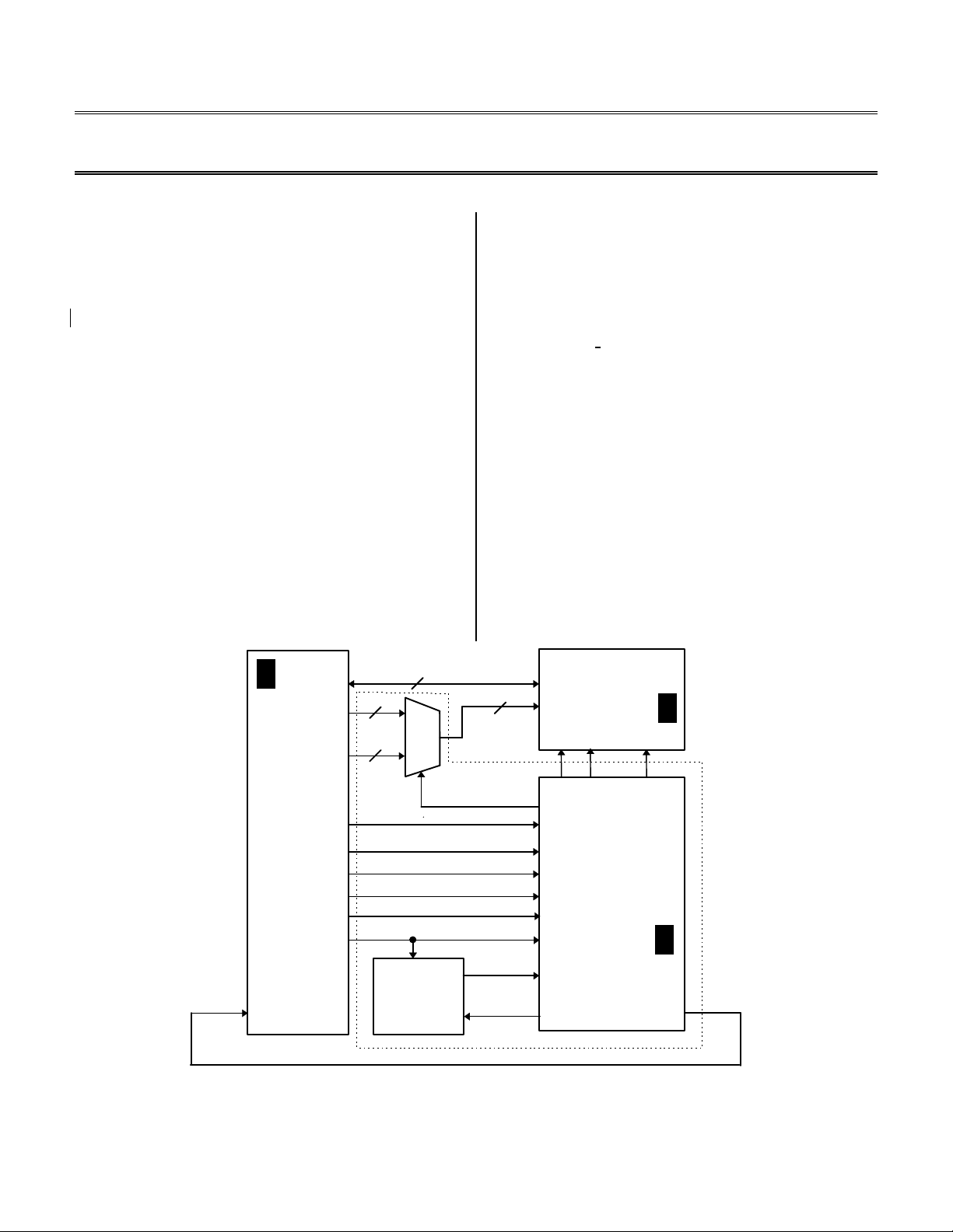
3. Mux, Refresh Timer, DRAM Controller:
These are three separate modules that are
programmed onto one 69 I/O pin Xilinx PLD
(XC95108-10PC84).
1
C
Mux
Shar
Refres
h
Figure 1: DRAM Interfacing Block Diagram
DRAM
2
DRAM
Controlle
3
a
DRAM is an ideal solution for mass data storage
210061910
620
2
r
43657
8
with high speed. However, DRAM requires page
swapping if an access crosses a page boundary. In
addition, DRAM requires refreshing so that data is
retained properly. This means an external
controller is needed to handle the interface between
the Sharc processor and the DRAM.
The controller receives input signals from the Sharc
on each memory access and asserts the right control
signals to the DRAM to read or write. Eleven 2:1
mux’s are used to select between column address
and row address depending on whether the
controller is doing a page swap or a normal
read/write. The refresh timer is responsible for
telling the controller when to refresh the DRAM.
II. Descriptions of the Refresh Timer and the
Controller
1. Refresh Timer:
Data sheets for this 4 Meg DRAM specify that all
2048 rows or pages need to be refreshed every
32ms. Spreading this task into equal intervals
shows that a new row needs to be refreshed every
15.625µs (32ms/2048). In this design, a refresh
request is generated by the timer every 15.525µs or
621 cycles if using a 40 Mhz clock.
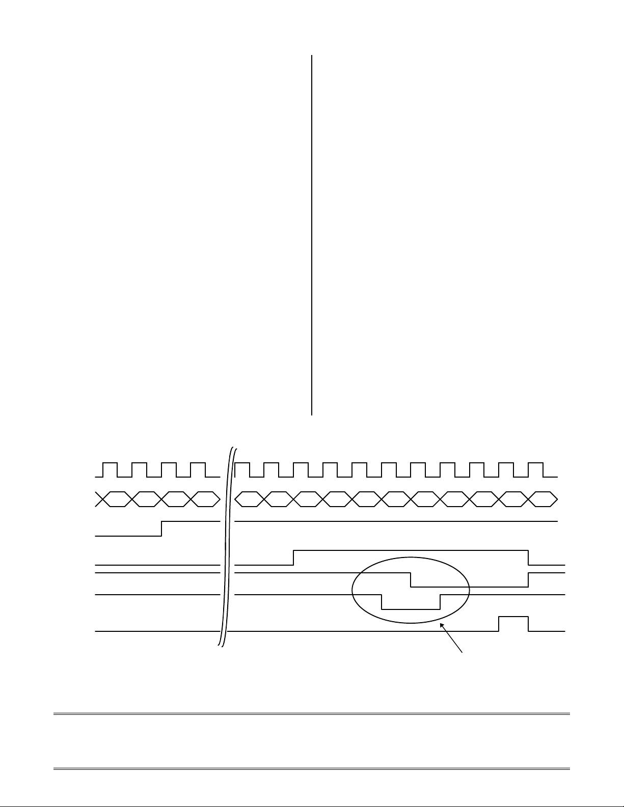
The refresh timer works as follows: during reset,
the counter is forced to zero from any state. When
reset is released, the counter will start counting up
to 620. At this point, the counter resets to zero and
starts counting again. At the same time, a refresh
request (RFQ) is asserted, signaling the controller
to refresh one row of the DRAM. There are
different ways of refreshing the DRAM. For this
design, CBR or CAS Before RAS method is used as
illustrated in the diagram below. First, the
controller returns CAS and RAS to high, if
necessary. Next, the controller brings CAS low, and
then RAS low in the next cycle. It is important that
RAS and CAS should remain high or low long
enough to meet the time specifications in the data
sheets. At the end of the refresh cycles, the
controller asserts RFC (refresh complete) to signal
the refresh timer to bring RFQ low.
Using the CBR refresh method, the user does not
have to worry about which row to refresh. The
DRAM itself has an internal counter that keeps
track of which row to refresh. Each time a CBR is
performed, this internal counter will increment by
one so that the next adjacent page is refreshed on
the next CBR.
By refreshing one row every 15.5µs, the entire 4
Meg DRAM will effectively be refreshed within
every 32ms.
Clkin
Counte
/Reset
RFQ
/RAS
/CAS
RFC
Figure 2: Dram Refreshing for One Row or Page
CBR or
CAS Before RAS
EE-44 Page 2
Notes on using Analog Devices’ DSP, audio, & video components from the Computer Products Division
Phone: (800) ANALOG-D or (781) 461-3881, FAX: (781) 461-3010, EMAIL: dsp.support@analog.com
2. DRAM Controller:
DRA
a. Normal Page Swap, Read, Write
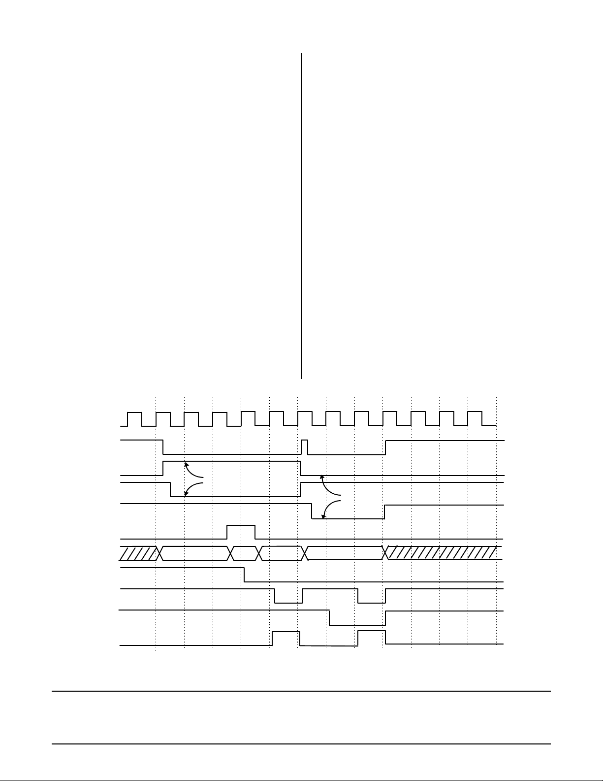
Figure 3 below illustrates the operations of an outof-page read followed immediately by a within-page
write. Note that the timing diagram given here
does not reflect precisely the number of cycles used
in the Abel file. Refer to discussion about
optimization toward the end of this document.
Upon the detection of /MS and Page, the controller
will assert MuxSel to select the row address. Then
/RAS is asserted low to latch in the new row
address. Note that MuxSel is clocked at the
negative clock edge so that row address is valid by
the falling edge of /RAS. Then, if this is a read,
/WR_DRAM is kept high while /CAS is asserted low.
During the same cycle, Ack is asserted high to
indicate the completion of one memory access. Note
that /RAS is held low so that the same page is
retained. It will remain low until a page swap is
required or a DRAM refresh is serviced.
In this example, a write follows immediately. Since
it is a same-page operation, only /CAS needs to go
low. /WR_DRAM is asserted this time for a write
cycle.
b. Refresh Request during a Read/Write:
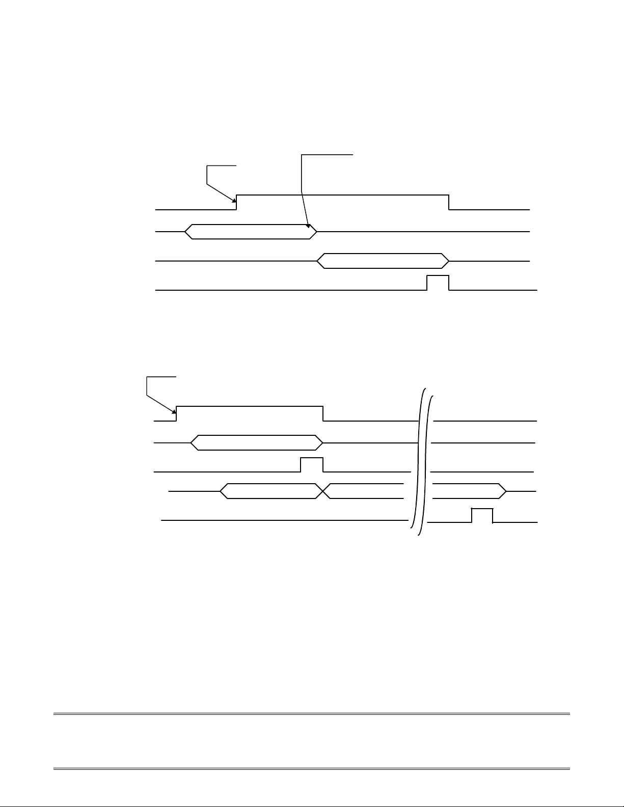
If the DRAM controller is servicing a memory
access when a refresh request occurs, the controller
will keep going to complete that memory read or
write before entering the refresh cycles. RFQ will
stay high until one row refresh has been done and
RFC is asserted. This is illustrated in Figure 4.
c. Memory Access Request during a Refresh
Service:
If the Sharc asserts /MS while the controller is
refreshing the DRAM, the controller will continue
to finish the refresh before servicing the memory
access. Without having Ack high during this time,
the Sharc will keep driving /MS, /RD or /WR, Data
and Address lines. Note that in this design, the
Sharc is configured to use Ack-only as waitstates.
Figure 5 illustrates this scenario.
Clkin
/MS
0
Page
Out-of-page READ
/RD
Within-page WRITE
/WR
MuxSel
AddrOu
Col Addr
Row
ColCol
/RAS
/CAS
/WR_
Ack
Figure 3: Page Swap, Read, Write
EE-44 Page 3
Notes on using Analog Devices’ DSP, audio, & video components from the Computer Products Division
Phone: (800) ANALOG-D or (781) 461-3881, FAX: (781) 461-3010, EMAIL: dsp.support@analog.com
RFQ
It’s time to
refresh !
Read/Write
Completes
/MS, /RD,
/RAS, /CAS
RFC
/RAS, /CAS
/MS, /RD,
RFQ
RFC
Ack
Reading/Writing
Refreshing
Figure 4: Refresh Request during a Read/Write
It’s time to
refresh !
Refreshing
Read/Write
Read/Write begins
. .
Figure 5: Memory Access Request during a Refresh Service
EE-44 Page 4
Notes on using Analog Devices’ DSP, audio, & video components from the Computer Products Division
Phone: (800) ANALOG-D or (781) 461-3881, FAX: (781) 461-3010, EMAIL: dsp.support@analog.com
d. Controller State Machine:
RFQ
RFQ
end of S15
end of S11
end of S10
end of S7
(regardless of Page)
/MS0, Page
/MS0Reset
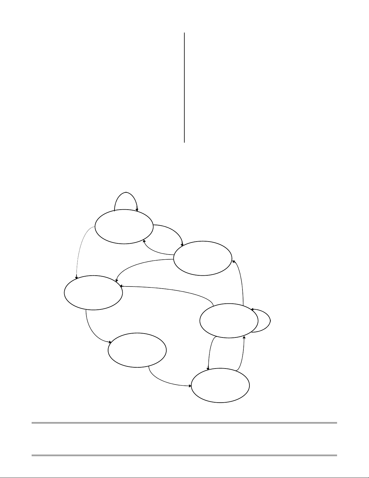
This DRAM controller is implemented as a Mealy
state machine and is programmed onto a Xilinx
PLD with 69 I/O pins. The state diagram on the
following page shows the flow of the design with
transitions from one state to another. Please refer
to the Abel source code for the output signals.
Several states in the state machine are used merely
to hold /CAS or /RAS low or high in order to meet
the time specifications. Further optimization could
be done to speed up the design as discussed in a
later section.
During the Idle/Reset cycle, the controller keeps
/RAS and /CAS high which will put the DRAM into
a low power mode. From here, the controller can
go to refresh cycles if RFQ is asserted or go to start
a memory access. Note that coming out of the idle
state, the controller needs to update the page in the
DRAM regardless of whether this is a out-of-page
access or not. The reason is that /RAS is no longer
held low during idle period.
In the state of Read/Write within Page, the
controller can remain here to wait for the next
memory access or go to refresh the DRAM if
necessary.
Page Swap
(S8..S10)
Idle/Reset
(S0)
/MS0,
Read/Write
after a Page Swap
(S11)
Refresh
(S1..S7)
/MS
(without Page)
Read/Write
within Page
(S12)
0
Extending
Cas/Ras
(S13..S15)
else
remain
EE-44 Page 5
Notes on using Analog Devices’ DSP, audio, & video components from the Computer Products Division
Phone: (800) ANALOG-D or (781) 461-3881, FAX: (781) 461-3010, EMAIL: dsp.support@analog.com
Figure 6: DRAM Controller State Diagram
III. Hardware Description
J6J3J21
J1
KIT
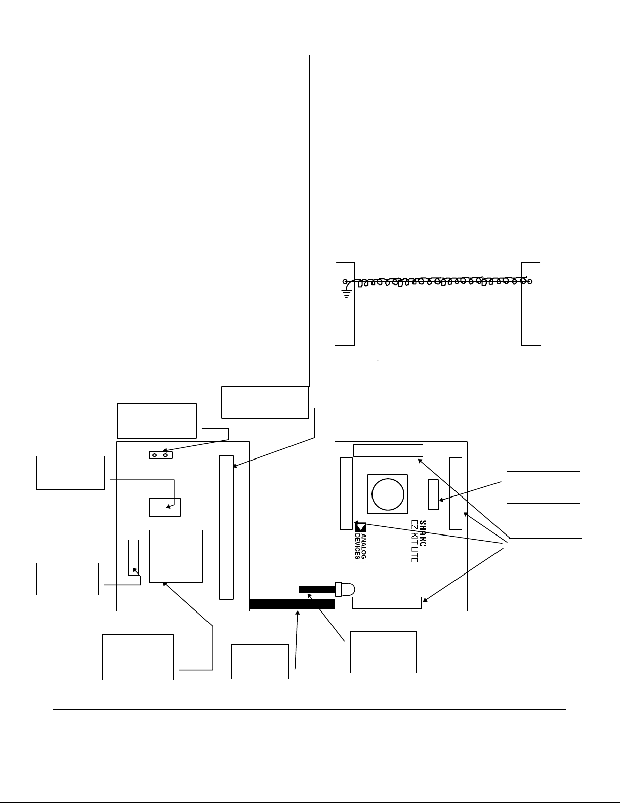
A prototype of this design has been built with the
layout shown in Figure 7 below.
On the left is the DRAM board with 2 major
components:
1. DRAM: This is placed along the long edge
close to the Sharc EZ-Kit Lite board so that
the lengths of the wires connected to the
Sharc EZ-Kit Lite board are minimized for
noise reduction purposes.
2. Xilinx PLD: This is the DRAM Controller.
The refresh timer and the mux’s are all
programmed onto this same PLD. The Abel
file attached with this document includes all
code and equations necessary to program
this PLD.
Other components include the following:
1. A JTAG connector that allows the users to
easily program the PLD using a parallel
EZJTAG download cable from Xilinx.
2. An optional socket to hold the Xtal if an
external clock is used.
3. Power connector. An external power source
that can provide at least 1.5A must be used
to satisfy the demand of the DRAM.
DRAM
External
(MT8D432M-6x)
power
On the right is the Sharc EZ-KIT Lite board with
four external connectors shown in the figures. All
the signals shown in Figure 1: DRAM Interfacing
Block Diagram are available from these connectors.
This board runs on its own power supply. However,
common ground is needed between the two boards.
At least one thick wire should be used to make this
connection between the ground plane of the DRAM
board and the ground pin of the power connector to
the Sharc EZ-KIT Lite board.
Twisted pairs of wires are used for all data lines,
address lines, and control signals with the looping
wire grounded to reduce signal interference. Same
method is used for the clock signal but with thicker
wire.
Figure 8: Twisted Pair of
Optional
Xtal Clock
EZ-ICE
Connector
Sharc EZ-Kit
Lite External
Xilinx
Connectors
JTAG
Xilinx PLD
(XC9510810PC84)
Common
Ground
Power to
Sharc EZ-
Figure 7: Components and Board Layout
EE-44 Page 6
Notes on using Analog Devices’ DSP, audio, & video components from the Computer Products Division
Phone: (800) ANALOG-D or (781) 461-3881, FAX: (781) 461-3010, EMAIL: dsp.support@analog.com

Each VDD pin on the DRAM and the PLD has two
decoupling capacitors of .02uF and 1.0uF in
parallel. On the pin where the power supply is
brought into the board, two capacitors of .1uF and
22uF are used.
Note that on the Sharc EZ-KIT Lite board, there is
an EZ-ICE connector which allows the users to
attach an EZ-ICE and use this emulator to debug
the DRAM Controller.
IV. Possible Design Modifications and
Improvement
*** Important Notes about This Design ***
However, the DRAM Controller has only been
tested with a 40Mhz clock taken from the Sharc EZKIT Lite board. This means there are two possible
improvements for speed.
1. 60 Mhz clock is used:
In this Design we use an external EPSON
Americana 60 Mhz Oscilator(SG-615PCV) in
addition to the other hardware to make the
controller function faster. In the Appendix of this
EE Note we provide
App. 1. Abel Source Code: consists of
equations to implement the refresh
timer, mux’ , and the state machine for
the controller. The Abel code has been
synthesized and fitted using the
Foundations Series Tool Suite
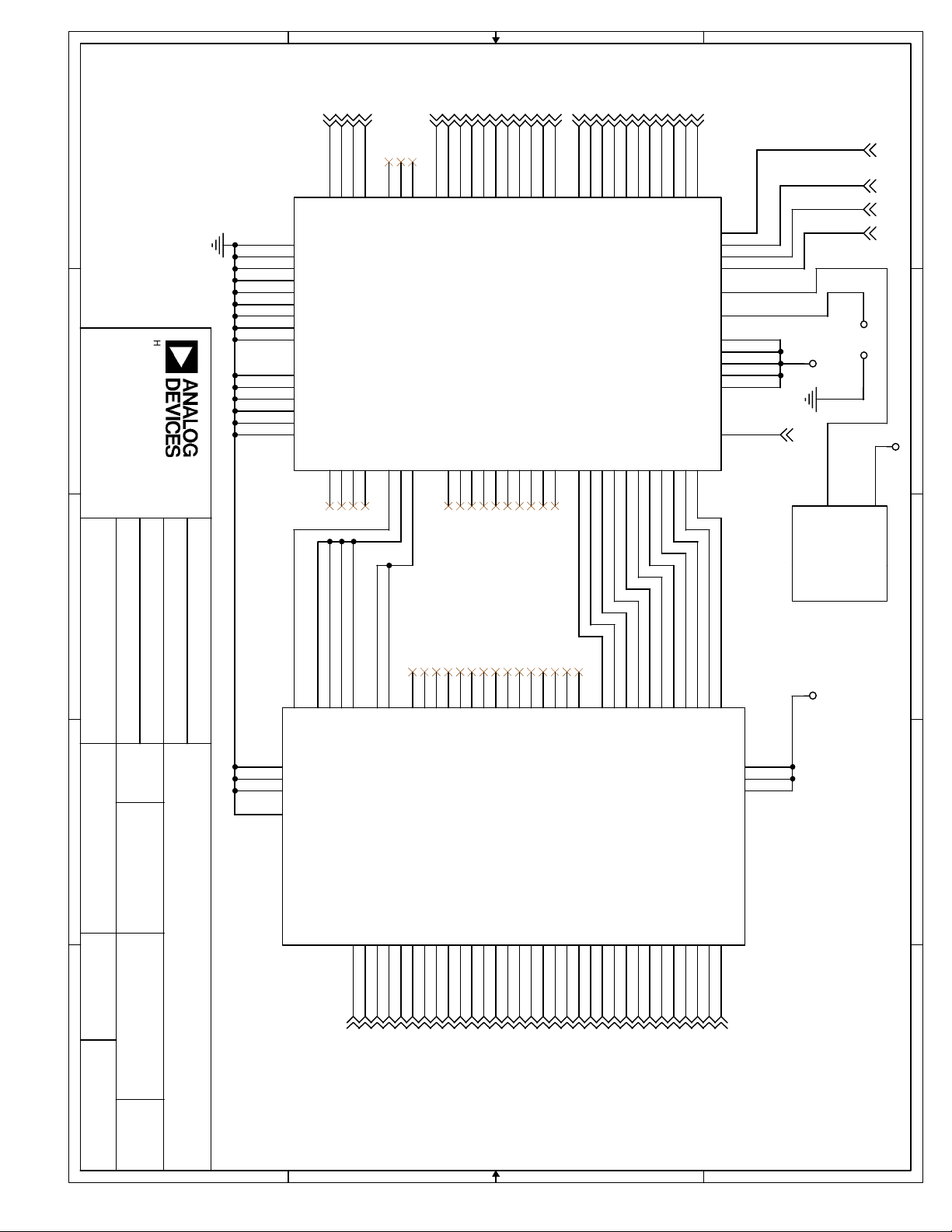
App. 2. Schematics: is drawn using OrCAD.
J1, J3, and J6 are the actual
connectors on the Sharc EZ-Kit Lite
board.
App. 3. Layout
App. 4. Overall Layout
It is also recommended to optimize the logic of the
state-machine for better performance, especially
those states that extend the /CAS and /RAS control
signals.
Of course, another solution to this design problem
would be changing the entire approach to a more
effective method. If the controller is run at a fast
clock speed, it is possible just to program waitstates
on the SHARC and not use the ACK signal at all. If
a refresh request occurs during a burst of write or
read cycles, the controller may assert the Suspend
Bus Tri-State (/SBTS) signal to halt the dsp, and
then service the refresh. This way the SHARC will
not occupy the address bus and data bus while the
controller is refreshing the DRAM. If there are
other external devices to the system, these devices
may make use of the bus while the dsp is halting.
/SBTS may also be used during a page swapping
cycle. The controller latches in the new row address
before asserting /SBTS. When the address lines of
the dsp become tri-stated, the controller puts back
the row address onto the bus and asserts /RAS to
update the page in the DRAM. Then, it releases
/SBTS to continue the memory access normally.
V. Conclusion
This design has been tested to work quite
successfully. However, this is not the optimal
design as far as speed is concerned. Once in a
while, it is still subjective to noise, especially when
all or most of the data lines switch to high at the
same time causing a few glitches on some control
signals. If someone tries to duplicate this process, it
is recommended that further measures be taken to
clean out such noises. For example, putting a
capacitor and a resistor (with calculated values) in
series near input pins to the Sharc might help
reduce reflection on these transmission lines.
2. 66Mhz or higher clock is used:
If a faster external clock is used as originally
intended for this design, then other considerations
have to be taken into account. The immediate
benefit would be speed. However, there will be
timing issues such as making Ack meet the setup
and hold time so that the Sharc can sample
correctly. Another potential problem is that
running a 66Mhz will introduce more noise to the
system, especially for a wire-wrapping board.
EE-44 Page 7
Notes on using Analog Devices’ DSP, audio, & video components from the Computer Products Division
Phone: (800) ANALOG-D or (781) 461-3881, FAX: (781) 461-3010, EMAIL: dsp.support@analog.com


Dramctrl
MODULE DramCtrl
title 'Dram Controller';
"Input signals"
Reset_ pin 81 istype 'reg';
DramClkin pin 9 istype 'reg'; "Ext 60MHz Cloc
k
MS0_ pin 53 istype 'reg';
RD_ pin 36 istype 'reg';
WR_ pin 35 istype 'reg';
Page pin 33 istype 'reg';
A00,A01,A02,A03,A04 pin 80,79,77,76,75 istype 'com';
A05,A06,A07,A08,A09,A10 pin 74,72,71,70,69,68 istype 'com';
A11,A12,A13,A14,A15 pin 67,66,65,63,62 istype 'com';
A16,A17,A18,A19,A20,A21 pin 61,58,57,56,55,54 istype 'com';
"Input/Output"
RFQ pin 50 istype 'reg'; "Timer's Outp
ut to Controller's Input"
RFC pin 51 istype 'reg'; "Controller's
Output to Timer's Input"
"Output signals"
RAS_ pin 24 istype 'reg';
CAS_ pin 25 istype 'reg';
WR_DRAM_ pin 26 istype 'reg';
Ack pin 34 istype 'reg'; "Ack needs to
be in sync with SHARC Clk
MuxSel pin 52 istype 'reg'; "H: RowAddr; L
: ColAddr
Y00,Y01,Y02,Y03,Y04 pin 11,12,13,14,15 istype 'com';
Y05,Y06,Y07,Y08,Y09,Y10 pin 17,18,20,21,23,19 istype 'com';
q0, q1, q2, q3 pin 43,44,45,46 istype 'reg'; "Variables for
State Machine
t0, t1, t2, t3, t4 pin 82,83,84,1,2 istype 'reg';
t5, t6, t7, t8, t9 pin 3,4,5,6,7 istype 'reg';
xepld property 'FAST ON'; "Special Setting for Xilinx CPLD
declarations
S0 = [0,0,0,0]; S1 = [0,0,0,1]; S2 = [0,0,1,0]; S3 = [0,0,1,1];
S4 = [0,1,0,0]; S5 = [0,1,0,1]; S6 = [0,1,1,0]; S7 = [0,1,1,1];
S8 = [1,0,0,0]; S9 = [1,0,0,1]; S10 = [1,0,1,0]; S11 = [1,0,1,1];
S12 = [1,1,0,0]; S13 = [1,1,0,1]; S14 = [1,1,1,0]; S15 = [1,1,1,1];
"Intermediate variables
"use the following line for actual code : cnt_ref = 930;
CNT_REF = t9 & t8 & t7 & !t6 & t5 & !t4 & !t3 & !t2 & t1 & !t0;
"use the following line for simulation : cnt_ref = 31;
"CNT_REF = !t9 & !t8 & !t7 & !t6 & !t5 & t4 & t3 & t2 & t1 & t0;
count = [t9,t8,t7,t6,t5,t4,t3,t2,t1,t0];
lowerAddr = [A10,A09,A08,A07,A06,A05,A04,A03,A02,A01,A00];
upperAddr = [A21,A20,A19,A18,A17,A16,A15,A14,A13,A12,A11];
fsmState = [q3,q2,q1,q0];
SCLR = !Reset_ # CNT_REF;
C,H,L,Z = .C.,1,0,.Z.;
equations
App. 1-1

Dramctrl
[q3,q2,q1,q0].clk = DramClkin;
[RAS_,CAS_,WR_DRAM_,Ack].clk = DramClkin;
[RFQ,RFC].clk = DramClkin;
[MuxSel].clk = !DramClkin;
[t0,t1,t2,t3,t4,t5,t6,t7,t8,t9].clk = DramClkin;
Ack.oe=Reset_; " This is used to disable Ack when EZ-Kit Lite is booting.
"This reset is separate from Sharc Reset. This is a temporary
"work around. So that the UART and the DRAM don't conflict.
"Below is the refresh timer:
t0 := (!t0) & !SCLR;
t1 := (t1 $ t0) & !SCLR;
t2 := (t2 $ (t1 & t0)) & !SCLR;
t3 := (t3 $ (t2 & t1 & t0)) & !SCLR;
t4 := (t4 $ (t3 & t2 & t1 & t0)) & !SCLR;
t5 := (t5 $ (t4 & t3 & t2 & t1 & t0)) & !SCLR;
t6 := (t6 $ (t5 & t4 & t3 & t2 & t1 & t0)) & !SCLR;
t7 := (t7 $ (t6 & t5 & t4 & t3 & t2 & t1 & t0)) & !SCLR;
t8 := (t8 $ (t7 & t6 & t5 & t4 & t3 & t2 & t1 & t0)) & !SCLR;
t9 := (t9 $ (t8 & t7 & t6 & t5 & t4 & t3 & t2 & t1 & t0)) & !SCLR;
RFQ := !RFC & ((CNT_REF # RFQ.FB) & Reset_);
"Shown here is the Multiplexer for Row and Column Addresses.
Y00 = (A00 & !MuxSel ) # (A11 & MuxSel);
Y01 = (A01 & !MuxSel ) # (A12 & MuxSel);
Y02 = (A02 & !MuxSel ) # (A13 & MuxSel);
Y03 = (A03 & !MuxSel ) # (A14 & MuxSel);
Y04 = (A04 & !MuxSel ) # (A15 & MuxSel);
Y05 = (A05 & !MuxSel ) # (A16 & MuxSel);
Y06 = (A06 & !MuxSel ) # (A17 & MuxSel);
Y07 = (A07 & !MuxSel ) # (A18 & MuxSel);
Y08 = (A08 & !MuxSel ) # (A19 & MuxSel);
Y09 = (A09 & !MuxSel ) # (A20 & MuxSel);
Y10 = (A10 & !MuxSel ) # (A21 & MuxSel);
state_diagram [q3,q2,q1,q0];
"******************Idle/Reset State*********************
State S0:
IF (!Reset_)
THEN S0 WITH {RAS_ := 1; CAS_ := 1; WR_DRAM_ := 1;}
ELSE IF (RFQ)
THEN S1 WITH {RAS_ := 1; CAS_ := 1; WR_DRAM_ := 1;}
ELSE IF (!MS0_)
THEN S8 WITH {RAS_ := 1; CAS_ := 1; WR_DRAM_ := 1;}
ELSE
Goto S0 WITH {RAS_ := 1; CAS_ := 1; WR_DRAM_ := 1;}
"******************Refreshing states********************
State S1:
IF (!Reset_)
THEN S0 WITH {RAS_ := 1; CAS_ := 1; WR_DRAM_ := 1;}
ELSE
Goto S2 WITH {RAS_ := 1; CAS_ := 1; WR_DRAM_ := 1;}
State S2:
IF (!Reset_)
THEN S0 WITH {RAS_ := 1; CAS_ := 1; WR_DRAM_ := 1;}
App. 1-2

Dramctrl
ELSE
Goto S3 WITH {RAS_ := 1; CAS_ := 0; WR_DRAM_ := 1;}
State S3:
IF (!Reset_)
THEN S0 WITH {RAS_ := 1; CAS_ := 1; WR_DRAM_ := 1;}
ELSE
Goto S4 WITH {RAS_ := 0; CAS_ := 0; WR_DRAM_ := 1;}
State S4:
IF (!Reset_)
THEN S0 WITH {RAS_ := 1; CAS_ := 1; WR_DRAM_ := 1;}
ELSE
Goto S5 WITH {RAS_ := 0; CAS_ := 1; WR_DRAM_ := 1;}
State S5:
IF (!Reset_)
THEN S0 WITH {RAS_ := 1; CAS_ := 1; WR_DRAM_ := 1;}
ELSE
Goto S6 WITH {RAS_ := 0; CAS_ := 1; WR_DRAM_ := 1;}
State S6:
IF (!Reset_)
THEN S0 WITH {RAS_ := 1; CAS_ := 1; WR_DRAM_ := 1;}
ELSE
Goto S7 WITH {RAS_ := 0; CAS_ := 1; WR_DRAM_ := 1; RFC := 1;}
State S7:
IF (!Reset_)
THEN S0 WITH {RAS_ := 1; CAS_ := 1; WR_DRAM_ := 1;}
ELSE IF (!MS0_)
THEN S8 WITH {RAS_ := 1; CAS_ := 1; WR_DRAM_ := 1;}
ELSE
Goto S0 WITH {RAS_ := 1; CAS_ := 1; WR_DRAM_ := 1;}
"*****************PageSwap State*****************************
State S8:
IF (!Reset_)
THEN S0 WITH {RAS_ := 1; CAS_ := 1; WR_DRAM_ := 1;}
ELSE
Goto S9 WITH {MuxSel := 1; RAS_ := 1; CAS_ := 1; WR_DRAM_ := 1;}
State S9:
IF (!Reset_)
THEN S0 WITH {RAS_ := 1; CAS_ := 1; WR_DRAM_ := 1;}
ELSE
Goto S10 WITH {MuxSel := 1; RAS_ := 1; CAS_ := 1; WR_DRAM_ := 1;}
State S10:
IF (!Reset_)
THEN S0 WITH {RAS_ := 1; CAS_ := 1; WR_DRAM_ := 1;}
ELSE
Goto S11 WITH {MuxSel := 1; RAS_ := 0; CAS_ := 1; WR_DRAM_ := 1;}
State S11:
IF (!Reset_)
THEN S0 WITH {RAS_ := 1; CAS_ := 1; WR_DRAM_ := 1;}
ELSE
Goto S12 WITH {MuxSel := 1; RAS_ := 0; CAS_ := 1; WR_DRAM_ := 1;}
"*****************Waiting for RD/WR State after PageSwap************
State S12:
App. 1-3

Dramctrl
IF (!Reset_)
THEN S0 WITH {RAS_ := 1; CAS_ := 1; WR_DRAM_ := 1;}
ELSE IF (!RD_)
THEN S14 WITH {RAS_ := 0; CAS_ := 0; WR_DRAM_ := 1; Ack := 0;}
ELSE IF (!WR_)
THEN S14 WITH {RAS_ := 0; CAS_ := 0; WR_DRAM_ := 0; Ack := 0;}
ELSE
Goto S0 WITH {RAS_ := 1; CAS_ := 1; WR_DRAM_ := 1;}
"*****************Waiting for RFQ or next mem access****************
State S13:
IF (!Reset_)
THEN S0 WITH {RAS_ := 1; CAS_ := 1; WR_DRAM_ := 1;}
ELSE IF (RFQ)
THEN S1 WITH {RAS_ := 1; CAS_ := 1; WR_DRAM_ := 1;}
ELSE IF (!MS0_ & Page)
THEN S8 WITH {RAS_ := 1; CAS_ := 1; WR_DRAM_ := 1;}
ELSE IF (!MS0_ & !Page & !RD_)
THEN S14 WITH {RAS_ := 0; CAS_ :=0; WR_DRAM_ := 1; Ack := 0;}
ELSE IF (!MS0_ & !Page & !WR_)
THEN S14 WITH {RAS_ := 0; CAS_ :=0; WR_DRAM_ := 0; Ack := 0;}
ELSE
Goto S13 WITH {RAS_ := 0; CAS_ := 1; WR_DRAM_ := 1;}
"*****************Extending CAS/RAS State****************************
State S14:
IF (!Reset_)
THEN S0 WITH {RAS_ := 1; CAS_ := 1; WR_DRAM_ := 1;}
ELSE IF (!RD_)
THEN S15 WITH {RAS_ := 0; CAS_ :=1; WR_DRAM_ := 1; Ack := 1;}
ELSE IF (!WR_)
THEN S15 WITH {RAS_ := 0; CAS_ :=1; WR_DRAM_ := 1; Ack := 1;}
ELSE
GOTO S0 WITH {RAS_ := 1; CAS_ := 1; WR_DRAM_ := 1;}
State S15:
IF (!Reset_)
THEN S0 WITH {RAS_ := 1; CAS_ := 1; WR_DRAM_ := 1;}
ELSE
GOTO S13 WITH {RAS_ := 0; CAS_ := 1; WR_DRAM_ := 1; Ack := 0;}
END DramCtrl
App. 1-4

4 4
g
g
g
ADDR9
ADDR10
ADDR11
3 3
ADDR7
ADDR8
ADDR4
ADDR5
ADDR6
ADDR1
ADDR2
ADDR3
ADDR0
TDO
TDI
2 2
ADDR12
ADDR13
ADDR14
ADDR15
ADDR16
ADDR17
ADDR18
ADDR19
ADDR20
ADDR21
1 1
TCK
TMS
A
HW DEVELOPMENT TOOLS ENG.
Computer Products Division
Analo
Three Technolo
P.O. Box 9106
Norwood, MA 02062-9106
B
C
Devices
y Way
Drafted By:
Approved By:
Created:
Modified: Sheet: of
Tuesday, June 30, 1998
Monday, December 08, 1997
Checked By:
C.K.P.
C.K.P.
Desi
ned By:
Controller
10
31
32
37
39
40
41
47
48
8
16
27
42
49
60 34
30
A00
A01
A02
A03
A04
A05
A06
A07
A08
A09
A10
A11
A12
A13
A14
A15
A16
A17
A18
A19
A20
A21
RFQ
RFC
MUXSEL
TDI
TDO
TMS
TCK
TIE
TIE
TIE
TIE
TIE
TIE
TIE
TIE
TIE
GND
GND
GND
GND
GND
GND ACK
Q2
Q3
46
45
Q1
Q0
44
WR_DRAM*
CAS*
43
25
26
RAS*
24
T9
T8
T7
T6
Controller
Y09
Y10
T0
T1
T2
T3
T4
T5
19
82
83
84
1234567
23
Y08
21
Y07
20
Y06
18
Y05
17
PAGE
WR*
RD*
MS0*
DRAMCLKIN
RESET*
VCC
VCC
VCC
VCC
VCC
Y00
Y01
Y02
Y03
Y04
11
12
13
14
15
80
79
77
76
75
74
72
71
70
69
68
67
66
65
63
62
61
58
57
56
55
54
50
51
52
28
59
29
U2
33
35
36
53
9
81
22
38
64
73
78
VDD
ACK
OUT
RD*PAGE MS0*WR*
1 2
JUMPER
JP1
3
1
60 Mhz
OE
VDDGND
Y1
Clock
A
B
VDD
42
C
12
13
14
15
16
17
18
28
31
32
19
11
29
33
35
36
37
38
45
46
48
66
68
697071
44
34
40
43
41
42
47
U1
A0
A1
A2
A3
A4
A5
A6
A7
A8
A9
A10
NC
NC
NC
NC
NC
NC
NC
NC
NC
NC
NC
PRD2
PRD3
PRD4
DQ25
DQ26
DQ27
52
54
56
DATA43
DATA41
DATA40
DATA42
NC
DQ22
DQ23
DQ24
25
27
50
DATA38
DATA39
DQ19
DQ20
DQ21
23
DATA36
DATA35
DATA34
DATA37
MT8D432M-6X
DRAM
DQ13
DQ14
DQ15
DQ16
DQ17
DQ18
61
63
65
357921
DATA30
DATA31
DATA33
DATA32
DATA29
DATA28
DQ11
DQ12
53
55
57
DATA27
DATA26
DQ10
DQ7
DQ8
DQ9
26
49
51
DATA25
DATA24
DATA22
DATA23
DQ5
DQ6
22
24
DATA21
DATA20
VCC
VCC
VCC
DQ1
DQ2
DQ3
DQ4
DATA18
DATA17
DATA19
10
30
59
246820
DATA16
RAS0*
RAS2*
CAS0*
CAS1*
CAS2*
CAS3*
WE*
DRAM
ControllerSchematic.dsn
D
E
A Internal 1.0
Schematic File Name:
Dwg. Scale is:
DRAM Controller
Controller
Size
CAGE Code CAS DWG NO Revision
1
72
39
67
VSS
VSS
VSS
PRD1
DQ30
DQ31
DQ32
60
62
64
DATA47
DATA45
DATA46
DQ28
DQ29
58
DATA44
VDD
controller with reset of EZKIT LITE.
NOTE: The Jumper is placed so that the Controller can be set
in reset state while the SHARC EZKIT LITE uses the ACK
signal. In other words the ACK of UART will not conflict
with ACK of Controller. If jumper isn't used the SHARC
EZ-ICE program will still work; simply connect Reset of
D
E
21

ADDR16
ADDR18
ADDR20
4 4
MS0*
1 1
2 2
3 3
ADDR11
ADDR13
ADDR10
ADDR8
ADDR5
ADDR3
ADDR1
A
HW DEVELOPMENT TOOLS ENG.
Computer Products Division
Analog Devices
Three Technology Way
P.O. Box 9106
Norwood, MA 02062-9106
B
Drafted By:
Approved By:
Created:
Modified: Sheet: of
Checked By:
Designed By:
TDO
TCK
TCK
111317
TDO
137
VDD
GND
Xilinx Jtag Header
TDI
TDI
TMS
TMS
J5
VDD
GND
HEADER 25X2
43 44
45 46
47 48
49 50
HEADER 20X2
41 42
39 40
37 38
39 40
ADDR0
35 36
37 38
31 32
33 34
35 36
ADDR6
ADDR4
ADDR2
29 30
31 32
33 34
25 26
27 28
29 30
ADDR9
ADDR7
RD*
23 24
25 26
27 28
17 18
19 20
21 22
23 24
ADDR17
ADDR12
ADDR15
ADDR14
PAGE
15 16
17 18
19 20
21 22
78
910
11 12
13 14
15 16
ADDR21
ADDR19
DATA45
DATA47
56
78
910
11 12
13 14
A
J3
12
34
56
VDD
B
DATA43
J1
12
34
Tuesday, June 30, 1998
Tuesday, December 09, 1997
C
ControllerSchematic.dsn
Schematic File Name:
D
Dwg. Scale is:
C.K.P.
Connectors
A Internal 1.0
Size
CAGE Code CAS DWG NO Revision
DRAM Controller
C.K.P.
GND
HEADER 25X2
DATA39
45 46
47 48
49 50
DATA32
DATA35
DATA37
39 40
41 42
43 44
DATA26
DATA28
DATA30
31 32
33 34
35 36
37 38
DATA20
DATA21
DATA23
23 24
25 26
27 28
29 30
ACK
WR*
DATA18
17 18
19 20
21 22
15 16
DATA46
56
78
910
11 12
13 14
C
VDD
DATA42
DATA44
D
J6
12
34
VDD
E
DATA36
DATA38
DATA40
DATA41
DATA29
DATA31
DATA33
DATA34
DATA22
DATA24
DATA25
DATA27
DATA16
DATA17
DATA19
E
22


SHARC
EZ-KIT LITE
EPROM
U7
J1
SHARC
a
J6J3

GROUND PLANE
PLEASE LOOK AT TABLE FOR EXACT PINOUT CONNECTIONS.
Connected to CPLD
Connected to Simm
DRAM Simm Module
Bottom View
RAS*,CAS*,WE*
Addr[0 :10]
Y[0:10 ]
BE42&BE43
60MHZ
CLK
BF1&BF2
AG42&AG43
J6
AC38&AD38
J1
Pin3
Ch ip
Bottom of
CPLD
Xilinx
AC19&AD19
Bottom of Header
JTAG S ignals
Solder Side
J3
AH1&AH2

VOLTAGE PLANE
PLEASE LOOK AT TABLE FOR EXACT PINOUT CONNECTIONS.
BF1&BF2
Bottom of He ader S older End
Top of
Chip
1
60MHZ
CLK
11
Xilinx
CPLD
J3
AH1&AH2
J1
AC19&AD19
Bottom of Hea der So lder En d
Top of JTAG Header
DRAM Simm Module Top View
Bottom of He ader S older End
BE42&BE43
AC38&AD38
J6
AG42&AG43


SHARC EZ-Kit Lite is upside down on bottom
Top Board is the Proto Board facing up.
 Loading...