Page 1

Engineer To Engineer Note EE 17
Notes on using Analog Devices’ DSP, audio, & video components from the Computer Products Division
Phone: (800) ANALOG-D or (781) 461-3881, FAX: (781) 461-3010, EMAIL: dsp.support@analog.com
ADSP-2187L Memory
Organization
Last Modified: 5/5/97
Introduction
The ADSP-2187L is a new addition to the ADSP-218x
series of DSP microprocessors. The ADSP-2187L shares
the same package pinout as the ADSP-2185/2186
processors. With 64K words of on-chip SRAM, the
ADSP-2187L performs most algorithms without using
external memory.
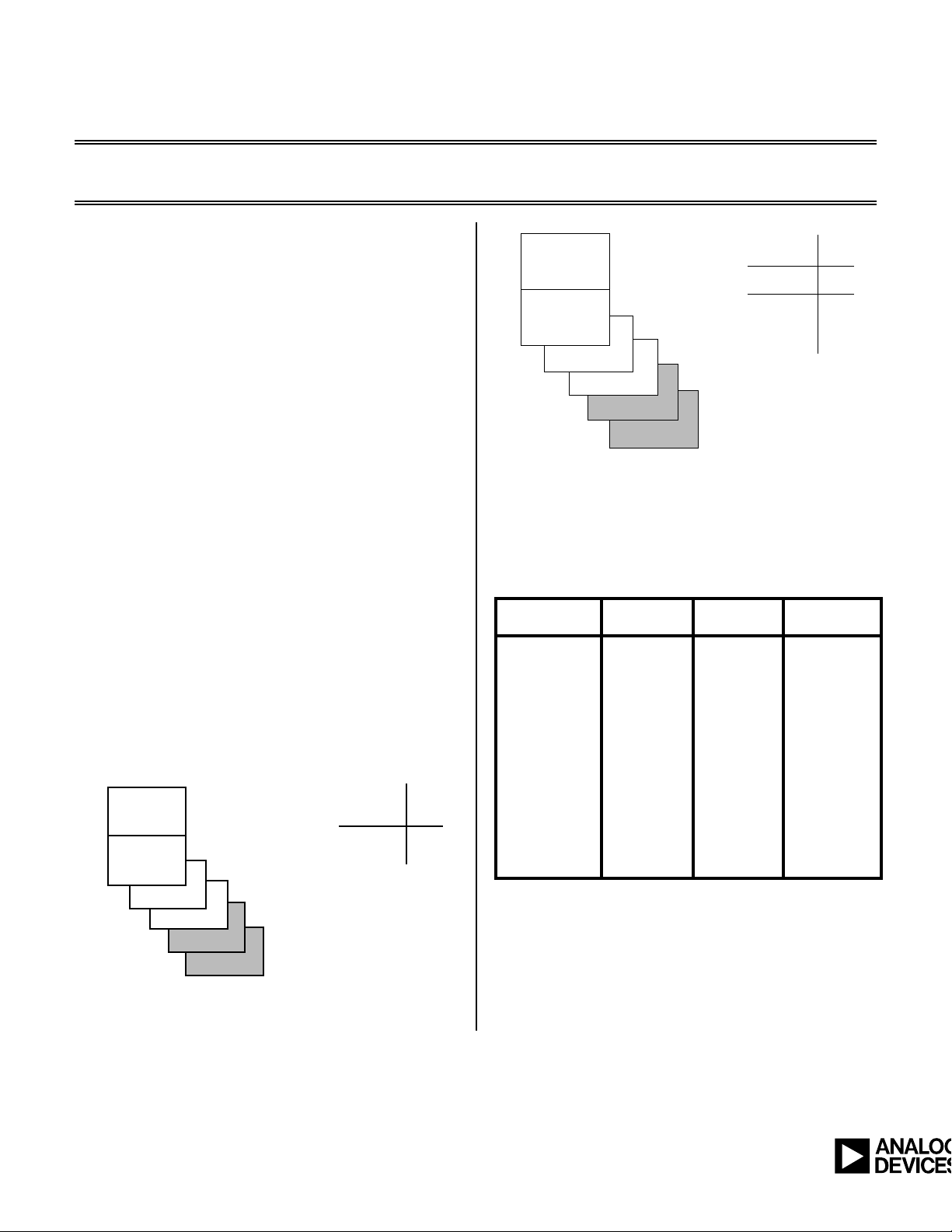
The processor’s internal memory is organized as: 32K
words on-chip Program Memory (PM) RAM and 32K
words on-chip Data Memory (DM) RAM.
The internal program memory is configured as one
permanent 8K segment and three 8K overlay segments
that are accessed by the PMOVLAY register.
Internal data memory is configured as one permanent 8K
segment and three 8K overlay segments that are accessed
by the DMOVLAY register. Two external 8K segments
are also available for both PM and DM and are accessed
through the PMOVLAY and DMOVLAY registers
respectively. This memory organization is shown in Table
1. Memory organization diagrams are shown in Figures 1
and 2.
PROGRAM MEMORY
PM MODE B = 0
ALWAYS
ACCESSABLE
AT ADDRESS
0x0000 - 0x1FFF
ACCESSABLE WHEN
INTERNAL
MEMORY
PM OVLAY = 0
ACCESSABLE WHEN
PM OVLAY = 4
EXTERNAL
MEMORY
0x2000 0x3FFF
ACCESSABLE WHEN
PM OVLAY = 5
ACCESSABLE WHEN
PMOVLAY = 1
ACCESSABLE WHEN
PMOVLAY = 2
0x2000 0x3FFF
0x2000 0x3FFF
0X2000 0X3FFF
2
0X2000 0X3FFF
2
Figure 1. Program Memory Organization
MODE B=0 ADDRESS
8K INTERNAL
PMOVLAY = 0, 4, 5
OR
8K EXTERNAL
PMOVLAY = 1, 2
8K
INTERNAL
0x3FFF
0x2000
0x1FFF
0x0000
DATA MEMORY
ALWAYS
ACCESSABLE
AT ADDRESS
0x2000 - 0x3FFF
ACCESSABLE WHEN
DM OVLAY = 0
INTERNAL
MEMORY
ACCESSABLE WHEN
DM OVLAY = 4
ACCESSABLE WHEN
DM OVLAY = 5
ACCESSABLE WHEN
EXTERNAL
MEMORY
DMOVLAY = 1
0x0000 0x1FFF
0x0000 0x1FFF
0x0000 0x1FFF
ACCESSABLE WHEN
DMOVLAY = 2
0X0000 0X1FFF
0X0000 0X1FFF
DATA MEMORY
32 MEMORY
MAPPED
REGISTERS
INTERNAL
8160
WORDS
8K INTERNAL
DMOVLAY = 0, 4, 5
EXTERNAL 8K
DMOVLAY = 1, 2
ADDRESS
0x3FFF
0x3FE0
0x3FDF
0x2000
0x1FFF
OR
0x0000
Figure 2. Data Memory Organization
The memory organization differs from other 218x family
devices; the internal overlay memory can now be accessed
by the IDMA and BDMA ports through two new registers
on the ADSP-2187L. These registers are discussed below.
Table 1 - Memory Overlay Pin Configurations
PMOVLAY/
DMOVLAY
0,4,5 Internal
1 External
2 External
MEMORY A13 A12:0
Overlay
Not
Applicable
Not
Applicable
0 13 LSB’s of
Overlay 1
Address
Between
0x2000 and
0x3FFF
1 13 LSB’s of
Overlay 2
Address
Between
0x2000 and
0x3FFF
Memory Modes
The ADSP-2187L, like the ADSP-2185/2186 can be
configured in one of two modes; Full Memory Mode or
Host Mode. Four mode pins are used to set memory
modes and booting. Mode selection information is located
in the ADSP-2187L data sheet.
Page 2

IDMA Operation (Host Mode)
Host mode provides full use of the IDMA port and access
to the full external data bus. However, the use of the
external address bus is limited to a single address pin, A0.
Additional hardware can be added to generate and latch
address signals.
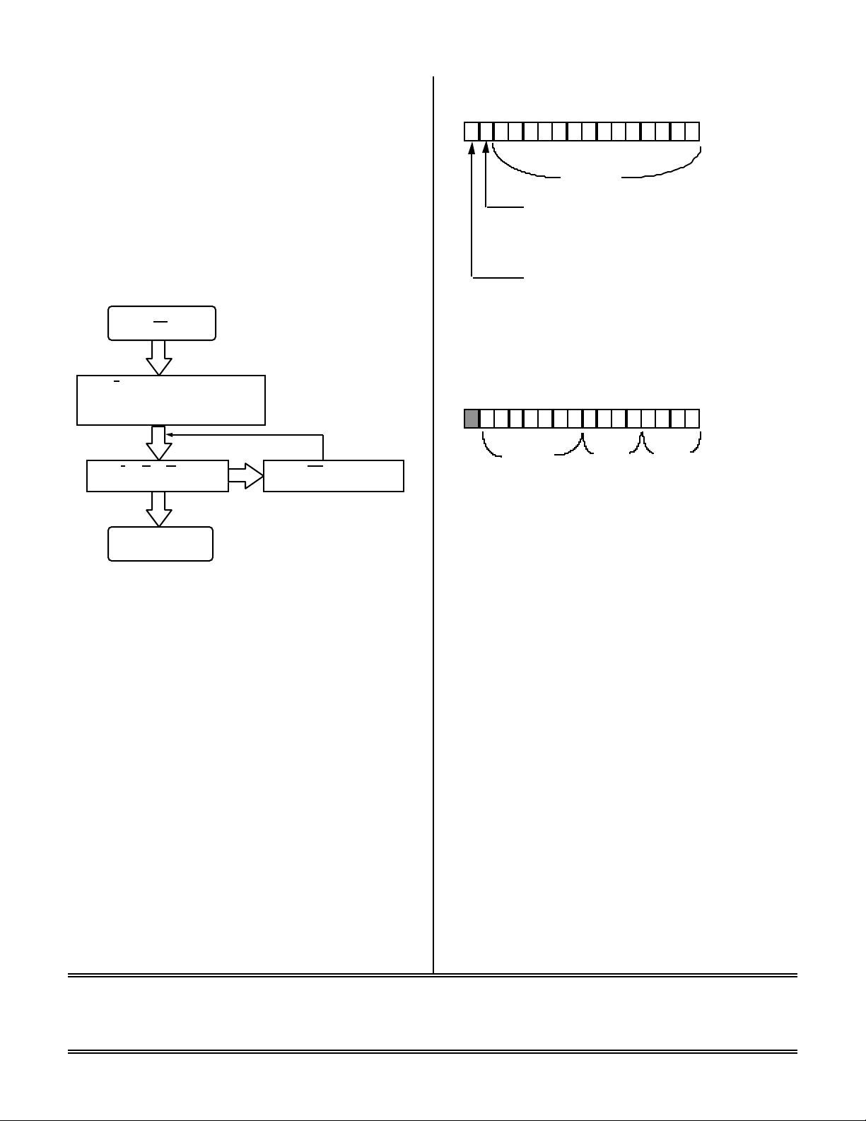
To use IDMA with the ADSP-2187L, the part must be
configured in Host Mode. The addition of the IDMA
OVLAY Register allows IDMA accesses to the internal
overlay memory. A typical IDMA transfer sequence is
shown in Figure 3.
Host Starts IDMA Transfer
Host checks IACK control line
to see if the DSP is busy.
IDMA CONTROL (U=Undefined at Reset)
15 14 13 12 11 10 9 8 7 6 5 4 3 2 1 0
U U U U U U U U U U U U U U U DM(0x3FE0)
U
IDMAA
ADDRESS
IDMAD
Destination Memory Type:
0=PM
1=DM
0=IDMA latches
address
1=IDMA latches
OVLAY memory
Figure 4. ADSP-2187L IDMA Control Register
Host uses IS and IAL control lines to latch either the
PM/DM OVLAY selection and/or the DMA starting address
(IDMAA) into the DSP’s IDMA Control Registers. The DSP
also can set the starting address and memory destination.
Continue
Host uses IS and IRD (or IWR) to read
(or write) DSP internal memory (PM or DM).
Done?
Host Ends IDMA Transfer
More?
Host checks IACK line to see if the DSP
has completed the previous IDMA operation.
Figure 3. ADSP-2187L IDMA Transfer Sequence
To write to the overlay memory via the IDMA port
requires two address latch cycles; one to latch the overlay
address and one to latch the starting address. If bit 15 of
the IDMA Control Register (figure 4) is set to 1, the
IDMA port latches the IDMA overlay information. If bit
15 is set to 0, the IDMA port latches the address, and bit
14 determines PM or DM access. If you do not latch the
overlay memory, the Overlay Register (figure 5) is set to
all zeros. If upgrading from a another 218x device to the
ADSP-2187L, no additional board hardware is necessary
for IDMA transfers.
When beginning a transfer from/to internal PM/DM make
sure the overlay page is latched if the program addresses
will increment into an overlay segment.
IDMA OVERLAY
15 14 13 12 11 10 9 8 7 6 5 4 3 2 1 0
0 0 0 0 0 0 0 0 0 0 0 0 0 0 0DM(0x3FE7)
RESERVED
SET TO 0
ID
DMOVLAY
ID
PMOVLAY
Figure 5. ADSP-2187L IDMA Overlay Register
The following code segment shows an example of writing
to the internal overlay memory through the overlay
register:
ax0=0xe000;
dm(0x3fe0)=ax0; /*latch overlay
page at DM
address 0x2000 */
ax0=0x0005;
dm(0x3fe7)=ax0; /*latch DM
internal
overlay */
**Note: The above sequence can occur in any order
The IDMA port on the ADSP-2187L has an additional
feature that allows the IACK signal to be configured either
as an open drain (can be “wire-or’ed”) or as always driven,
depending on the state of the MODE D pin. This is useful
for applications that require more than one ADSP-2187L
to be connected by their IACK pins. Mode selection can
be found in the ADSP-2187L Data Sheet.
BDMA Operation (Full Memory Mode)
EE-17 Page 2
Notes on using Analog Devices’ DSP, audio, & video components from the Computer Products Division
Phone: (800) ANALOG-D or (781) 461-3881, FAX: (781) 461-3010, EMAIL: dsp.support@analog.com
Page 3

If the ADSP-2187L is configured for full memory mode,
all address and data lines are available and the processor
boots from the BDMA port (the IDMA port is disabled).
I/O capability is retained in full memory mode as is access
to the external data and address buses.
The byte memory space on the ADSP-2187L is an 8-bit
wide external memory space which allows up to 4 Mbits
of ROM or RAM to be used. Writes to internal memory
are done using the Byte DMA Controller. The part must
be configured for Full Memory Mode to use the BDMA
port.
The BDMA controller of the ADSP-2187L allows access
to the internal overlay segments through four BDMA
Overlay bits (7:4) in the BDMA Control Register (figure
6).
BDMA CONTROL
15 14 13 12 11 10 9 8 7 6 5 4 3 2 1 0
0 0 0 0 0 0 0 0 0 0 0 1 0 0 0 DM(0x3FE3)0
BMPAGE
BDMA
OVERLAY
BITS
BTYPE
BDIR
0=LOAD FROM BM
1=STORE TO BM
BCR
0=RUN DURING BDMA
1=HALT DURING BDMA
The following code segment demonstrates how to set up
BDMA registers for a BDMA access to internal overlay
memory.
ax0=0x0048;
dm(0x3fe3)=ax0; /* start BDMA
transfer from page
0, write to
internal PM overlay,
use 24-bit words
*/
ax0=0x0000;
dm(0x3fe2)=ax0; /* load
external addresses beginning
at 0x0000 */
ax0=0x2000;
dm(0x3fe1)=axo; /* start
internal addresses at 0x2000
*/
Figure 6. ADSP-2187L BDMA Control Register
ax0=0x0200;
dm(0x3fe4)=axo; /* set the count
equal to 512 words */
EE-17 Page 3
Notes on using Analog Devices’ DSP, audio, & video components from the Computer Products Division
Phone: (800) ANALOG-D or (781) 461-3881, FAX: (781) 461-3010, EMAIL: dsp.support@analog.com
 Loading...