

Page 1
a
a Engineer To Engineer Note EE-150
aa
Technical Notes on using Analog Devices’ DSP components and development tools
Phone: (800) ANALOG-D, FAX: (781) 461-3010, EMAIL: dsp.support@analog.com, FTP: ftp.analog.com, WEB: www.analog.com/dsp
executable so that it integrates the end-application.
In-circuit programming a boot-image into the
FLASH on the ADDS-21161N-EZLITE
Submitted by Matthew Walsh Jan 2002
The final step is to download this flash-programming
executable to the DSP and run it!
1. Build the End Application
Overview
The ADSP-21161N, like most re-programmable
processors, requires internal program-code and data
to be boot-loaded upon power-up. This code&data
can either be supplied by a host system (i.e. hostboot, link-port boot, JTAG connection, etc.) or it can
be stored in an on-board non-volatile memory device
such as a ROM or FLASH. The 21161N EZ-Kit Lite
evaluation board enables the DSP to boot in any of
these ways, but the only one that allows standalone
operation (without connection to a PC) is PROM
Using the USB Debug-Agent, a JTAG Emulator,
and/or the VisualDSP++ Simulator, one can write
and test the end-application. As previously
mentioned, the end application in
blink.asm
toggles LED2-LED7 on the board. To verify that this
routine and one’s board is functional, activate an EZKit Lite debug-target in the IDDE and then open
blink.dpj. Next load the executable blink.dxe
(in the /
executable is loaded, simply hit run (
FLASH/debug directory). Once this
<F5> ) and
watch the LEDs.
booting. This is supported by a 512KB FLASH
memory device from ST Microdevices
(M29W040B).
This example shows how the ADSP-21161N can be
used to program an application into the FLASH. This
“in-circuit programming” (as opposed to burning the
flash before it is placed on the board) is most
frequently used to perform software or firmware
updates to systems already deployed in the field.
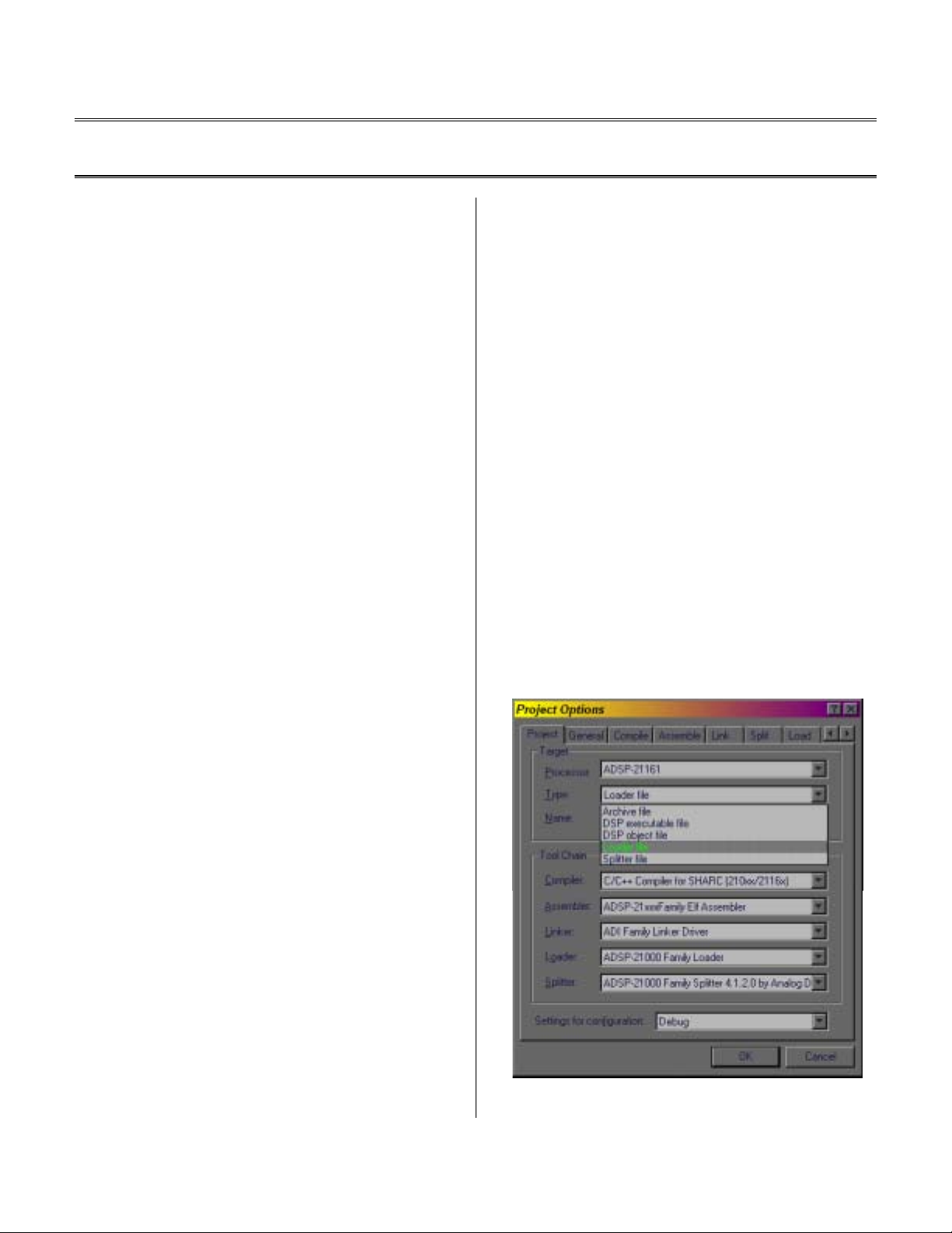
2. Create the PROM Boot-Image
With the end-application verified, we then use
VisualDSP++’s Loader to generate a boot-image
from our source code. To do this, we simply go to
the Project Options page of
blink.dpj and select
“Loader file” as the output file type (Figure-1.)
Doing this requires two separate sets of code: First, it
requires a software routine to program data into the
FLASH, and second, the end application that will
ultimately be boot-loaded and run by the DSP.
In this example, a generic FLASH programming
algorithm is contained in
prog-flash.asm, and the
dummy end-application is a simple LED toggling
routine in
as the data payload that
blink.asm. (This blink routine will serve
prog-flash.asm will
program into the FLASH.)
From start to finish, the attached code example
demonstrates the four general steps involved with
this in-circuit FLASH programming. First, the endapplication is written and debugged (here,
blink.dpj). The second step is to generate a
PROM boot-image (
The third step is to re-build the flash-programming
Copyright 2000, Analog Devices, Inc. All rights reserved. Analog Devices assumes no responsibility for customer product d esign or the use or ap plication of customers ’ products or
for any infringements of patents or rights of others w hich may result fro m Analog Devices assist ance. All trademarks and logos are property of their respective holders. Information
furnished by Analog Devices Applications and Development Tools Engineers is believed to be accurate and reliable, however no responsibility is assumed by Analog Devices
regarding the technical accuracy of the content provided in all Analog Devices’ Engineer-to-Engineer Notes.
blink.ldr) from that code.
Figure 1. Loader file as the output file Type
Page 2
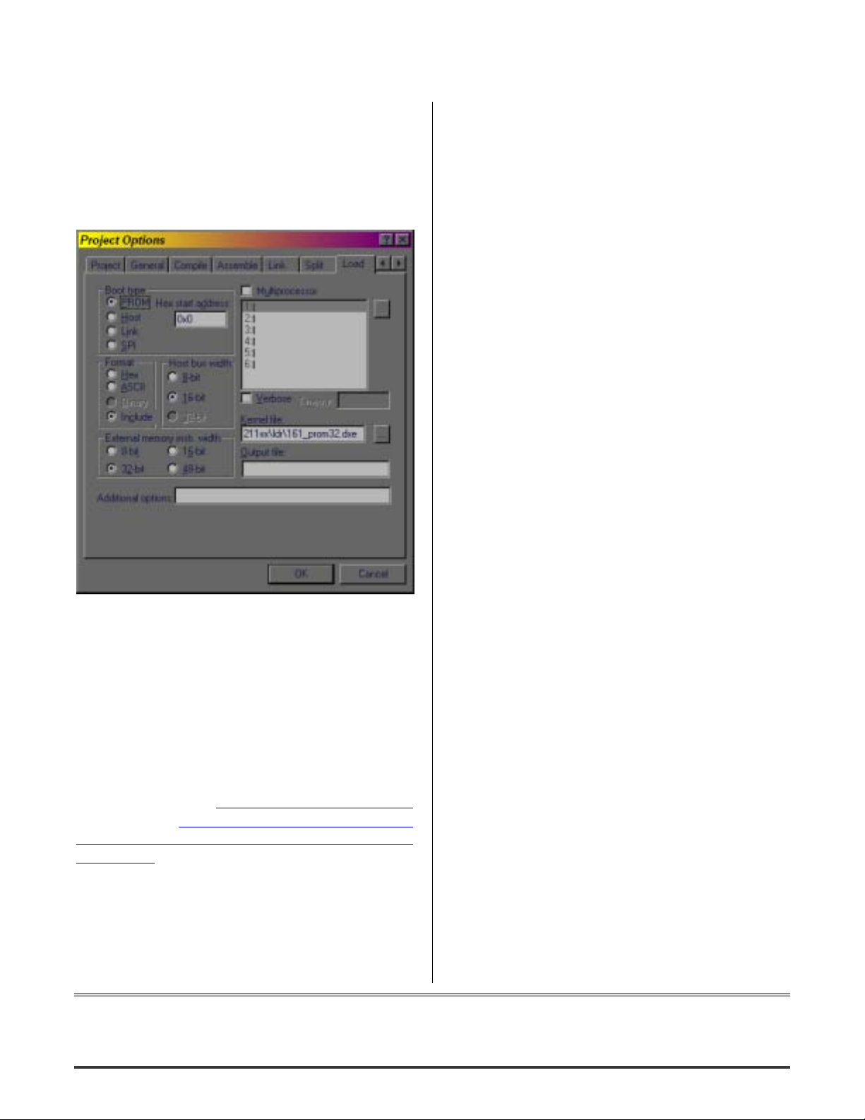
The .LDR file that we are about to generate is
ultimately going to be included into the flashprogramming routine as an array. To this end, the
.LDR file should be in the “Include” format
(essentially comma-delimited ASCII) with each word
being 16-bits, as can be seen in Figure-2.
Figure 2. Configure the .LDR file under the Load tab
Also, if you have any code that executes directly
from external memory, be sure to enter the width of
the external memory. Otherwise, just hit OK and
then Rebuild All. This will rebuild the project
according to the new Project Options and will
generate
input.ldr.
Additional information on generating Loader files for
the ADSP-21161 can be found in our online EZAnswers database:
http://www.analog.com/dsp/EZAnswers
and in EE-137: Executing Code Directly from 8, 16,
32 or 48 Bit External Memory Devices using the
ADSP21161.
3. Rebuild the Flash-Programming app.
The last step is to modify the flash-programming
application to include the recently generated
input.ldr. To do this, close input.dpj and open
programmer.dpj where one will find prog-
flash.asm.
In this file, we simply declare an array
in a section mapped to external memory and initialize
it with the payload LDR file. To use the example
end-application (blink), this is done as follows:
.section/dm sdram_sec;
.var input[]= ".\debug\blink.ldr";
(The linker description file [.
all
sdram_sec object sections to an external
memory segment [
mem_sdram])
LDF] is then used to map
Now, with the correct payload file specified, we
simply Rebuild the project to generate the flashprogramming executable (
prog-flash.dxe).
4. Programming the FLASH
The six LED’s are used to provide feedback on the
progress of the FLASH programming. Once we
download and run
prog-flash.dxe, all six LED’s
will blink simultaneously to indicate “I’m alive and
running.” Next, as each of the five steps to program
the FLASH complete, an LED either illuminates to
indicate that it was successful or blinks rapidly if it
has failed.
The five stages are as follows:
1) Verify the payload file size < 512KB.
2) Reset the flash and verify the device ID
3) Erase the Flash
4) Write the payload LDR file into the FLASH
5) Verify the data
If all five stages are successful, FLAG9 (LED2) is
then illuminated to indicate that the in-circuit FLASH
programming was successful.
Additional Notes:
1) EZ-Kit boards before revision 2.0 require a minor
modification to access the flash with the DSP.
Resistors R186 and R154 must be removed. (In these
alpha revisions of the board, the Cypress USB
controller is also connected to the FLASH device.
These two resistors connect the /RD and /WR lines of
the FLASH to the Cypress, and unless removed, will
prevent these signals from being driven low by the
DSP.)
EE-xx Page 2
Technical Notes on using Analog Devices’ DSP components and development tools
Phone: (800) ANALOG-D, FAX: (781)461-3010, EMAIL: dsp.support@analog.com, FTP: ftp.analog.com, WEB: www.analog.com/dsp
Page 3

2) The PROM boot kernels that ship with VisualDSP++
2.0 improperly program the ROM Boot Waitstates in
the WAIT register to have zero waitstates. Using one
of these original kernels will cause the PROM boot to
fail if the external port is run at more than 25MHz. To
avoid this, either use an updated boot-kernel or
configure the Clock Mode Jumpers (JP21) to operate
the external port no faster than 25MHz. The incorrect
WAIT initialization at the top of the kernel (part of the
SDRAM intialization) can be replaced with the
following instructions if a fixed kernel is unavailable:
USTAT1 = 0x01C00000;
dm(wait) = USTAT1;
3) In this example, we initialize the payload buffer,
input[] at build time, however in a real system, this
buffer would be initialized sometime during execution.
The new FLASH data could be imported from a serialport, link-port or SPI port, or it could be placed into
memory by an onboard host processor.
4) In VisualDSP++ 2.0, the only way to view the contents of
the FLASH is to open a two-column memory window and
then go to ( <CTRL-G> ) the starting address, which for the
EZ-Kit Lite is 0x400 0000. Then the contents of the flash
will be displayed as the eight (8) least significant bits at each
address.
5) To automate the debug process, programmer.tcl
contains TCL commands to build blink.dpj, then open
programmer.dpj, and then build programmer.dpj.
To use this TCL script, make any changes required to the
end application (in this case blink.asm) and then from
the File menu select Load TCL Script. VisualDSP++ 2.0
provides TCL help including a syntax guide and extensive
examples.
References:
M29W040 FLASH Datasheet:
http://eu.st.com/stonline/books/pdf/docs/6583.pdf
Appendix A: Source Code:
/************************ Blink.asm ********************************************/
// Toggles LED's up and down
/*******************************************************************************/
#include <def21161.h>
#define JINX 0x1FF000 // wait between each LED
#define PAUSE 0xfffFFF // wait between consecutive sweeps
.section/pm code_sec;
start:
wayback:
up: r2=r2+1;
down: nop;
pause: nop;
ustat1=dm(IOFLAG);
bit set ustat1 FLG4O|FLG5O|FLG6O|FLG7O|FLG8O|FLG9O;
dm(IOFLAG)=ustat1;
r2=-3;
// count up
lcntr = 9; do up until lce;
r0 = DM(IOFLAG);
r0 = btgl r0 by r1; /* toggle flag r1*/
r0 = btgl r0 by r2; /* toggle flag r1*/
DM(IOFLAG) = r0;
lcntr=JINX; do delay until lce; /*wait*/
delay: nop;
r1 = r1 + 1; /* increment which flag is toggled*/
// count down
lcntr = 9; do down until lce;
r1 = r1 - 1; /* increment which flag is toggled*/
r2=r2-1;
r0 = DM(IOFLAG);
r0 = btgl r0 by r1; /* toggle flag r1*/
r0 = btgl r0 by r2; /* toggle flag r1*/
DM(IOFLAG) = r0;
lcntr=JINX; do delay2 until lce; /*wait*/
delay2:nop;
lcntr = PAUSE; do pause until lce;
EE-xx Page 3
Technical Notes on using Analog Devices’ DSP components and development tools
Phone: (800) ANALOG-D, FAX: (781)461-3010, EMAIL: dsp.support@analog.com, FTP: ftp.analog.com, WEB: www.analog.com/dsp
Page 4

jump wayback;
/********************** END BLINK.ASM ***************************************/
/**************************** prog-flash.asm *********************************
This program writes a .LDR file into the flash on ADDS-21161N-EZLITE. The .LDR
file should be in the "INCLUDE" format with a "HOST BUS WIDTH" (meaning the
word width) of 16.
LED status:
FLAG4 = LDR verified to fit in flash (Flash_File_Size OK)
FLAG5 = Read manufacturer and device ID (Flash_Auto_Select OK)
FLAG6 = FLASH erased (Flash_Chip_Erase OK)
FLAG7 = LDR Programming complete (Flash_Write_Data OK)
FLAG8 = All data verified correct (Flash_Verify_Data OK)
FLAG9 = ALL OK
*****************************************************************************/
#include <def21161.h>
#define FlashStartAddress 0x4000000 //Flash starting address. Mapped to MS1
.section/dm sdram_sec;
.var input[]= "debug\blink.ldr"; //kernel in 16-bit include format
// program memory code
.segment/pm code_sec;
start:
r0 = 0; // data to write to flash
r1 = 0; // data read from flash
r2 = 0; // mask value
r3 = 0; // Manufacturer ID read
r4 = 0; // Device ID read
r5 = 0; // data read from file
r6 = 0; // temp
r7 = 0; // timeout
r8 = 0; // polling1
r9 = 0; // polling2
r10 = 0; // finished
r11 = 0; // file flag
r12 = 0; // device flag
r13 = 0; // erase flag
r14 = 0; // write flag
r15 = 0; // verify flag
//set flags as outputs
ustat1=dm(IOFLAG);
bit set ustat1 FLG4O|FLG5O|FLG6O|FLG7O|FLG8O|FLG9O;
dm(IOFLAG)=ustat1;
//toggle flags (set to 1 = illuminated)
lcntr=3, do (pause2 + 1) until LCE;
bit set ustat1 FLG4|FLG5|FLG6|FLG7|FLG8|FLG9;
dm(IOFLAG)=ustat1;
lcntr = 0xFFF000; do pause1 until lce;
pause1:nop;
bit clr ustat1 FLG4|FLG5|FLG6|FLG7|FLG8|FLG9;
dm(IOFLAG)=ustat1;
lcntr = 0xFFF000; do pause2 until lce;
pause2: nop;
nop;
call Flash_File_Size; // Checks for proper file size
call Flash_Reset; // reset the flash device
call Flash_Auto_Select; // read manufacturer and device ID
call Flash_Chip_Erase; // erase the flash
call Flash_Write_Data; // write data to the flash
call Flash_Verify_Data; // verify correct data was written
// all pass
bit set ustat1 FLG9;
dm(IOFLAG)=ustat1;
idle;
EE-xx Page 4
Technical Notes on using Analog Devices’ DSP components and development tools
Phone: (800) ANALOG-D, FAX: (781)461-3010, EMAIL: dsp.support@analog.com, FTP: ftp.analog.com, WEB: www.analog.com/dsp
Page 5

Flash_Write_Data:
Flash_Verify_Data:
ReadnCheck: nop; // used to flush the pipe
r14 = 1; // set error flag
i0 = FlashStartAddress; // set DAG to starting address of flash
m0 = 1; // set increment value
m7 = 1; // set increment value
i7 = input + 1; // set DAG to starting address of buffer with data from the file
// (ignore first word of .LDR which is address from –p switch)
r5=length(input)-1; // # 16bit words (see previous instruction/comment)
r5=r5+r5; // # 8-bit writes
lcntr = r5;
do Flash_Write - 1 until lce; // do this loop until all the data has been written
call Flash_Program_Unlock; // unlock the flash so we can write data to it
r5 = dm(i7,m7); // read 16 bits of valid data from the buffer
dm(i0,m0) = r5; // write the lower 8 bits of data to the flash
call data_polling; // check to see that the command completed
r5 = lshift r5 by -8; // shift data 8-bits to the right
call Flash_Program_Unlock; // unlock the flash so we can write data to it
dm(i0,m0) = r5; // write the lower 8 bits of data to the flash
call data_polling; // check to see that the command completed
Flash_Write:
r14 = 2; // clear error flag
call Light_LEDs; // light LED's to show status
rts; // return to where the function was called from
r15 = 1; // set error flag
i0 = FlashStartAddress; // set DAG to starting address of flash
i1 = (input+1); // set DAG to starting address of payload-buffer
lcntr = length(input) - 1; // sets the number of reads
r2 = 0xff; // mask value
do ReadnCheck-1 until lce; // do this loop until all the data has been verified
r1 = dm(i0,m0); // read a byte from flash
r1 = r1 and r2; // save valid portion
r6 = r1; // store in temp
r1 = dm(i0,m0); // read a second byte from flash
r1 = r1 and r2; // save valid portion
r1 = lshift r1 by 8; / shift valid portion left 8 bits
r6 = r6 OR r1; // store in temp
r5 = dm(i1,m0); // read 2 bytes from file
comp (r5,r6); // compare file against flash
if ne jump error; // if not equal there was an error
r15 = 2; // clear error flag
call Light_LEDs; // light LED's to show status
rts; // return to where the function was called from
Flash_File_Size:
Flash_Reset:
r11 = 1; // set error flag
r5 = r0; // read the amount of bytes to program
r6 = 524288; // size of flash is 512K
comp (r5, r6);
if ge jump error; // verify filesize is smaller than flash
r11 = 2; // clear error flag
call Light_LEDs; // light LED's to show status
rts;
r0 = 0xaa;
dm(FlashStartAddress + 0x555) = r0; // 1st operation
r0 = 0x55;
dm(FlashStartAddress + 0x2aa) = r0; //2nd operation
r0 = 0xf0;
EE-xx Page 5
Technical Notes on using Analog Devices’ DSP components and development tools
Phone: (800) ANALOG-D, FAX: (781)461-3010, EMAIL: dsp.support@analog.com, FTP: ftp.analog.com, WEB: www.analog.com/dsp
Page 6

dm(FlashStartAddress) = r0; //3rd operation
rts;
Flash_Auto_Select:
Flash_Chip_Erase:
r12 = 1; // set error flag
r0 = 0xaa;
dm(FlashStartAddress + 0x555) = r0; // 1st operation
r0 = 0x55;
dm(FlashStartAddress + 0x2aa) = r0; // 2nd operation
r0 = 0x90;
dm(FlashStartAddress + 0x555) = r0; // 3rd operation
r2 = 0xff; // used to mask the byte of data read from the flash
r3 = 0x20; // Manufacturer Code for ST Micro
r4 = 0xe3; // Device Code for M29W040B
r1 = dm(0x4000000); // reads the Manufacturer Code
r1 = r1 and r2;
comp (r1, r3);
if ne jump error; // verify correct value read
r1 = dm(0x4000001); // reads the Device Code
r1 = r1 and r2;
comp (r1, r4);
if ne jump error; // verify correct value read
r12 = 2; // clear error flag
call Light_LEDs; // light LED's to show status
rts;
r13 = 1; // set error flag
r0 = 0xaa;
dm(FlashStartAddress + 0x555) = r0; // 1st operation
r0 = 0x55;
dm(FlashStartAddress + 0x2aa) = r0; // 2nd operation
r0 = 0x80;
dm(FlashStartAddress + 0x555) = r0; // 3rd operation
r0 = 0xaa;
dm(FlashStartAddress + 0x555) = r0; // 4th operation
r0 = 0x55;
dm(FlashStartAddress + 0x2aa) = r0; // 5th operation
r0 = 0x10;
dm(FlashStartAddress + 0x555) = r0; // 6th operation
call data_polling; // check to see that the command completed
r13 = 2; // clear error flag
call Light_LEDs; // light LED's to show status
rts; // return to where the function was called from
Flash_Program_Unlock:
data_polling:
Check:
r0 = 0xaa;
dm(FlashStartAddress + 0x555) = r0; // 1st operation
r0 = 0x55;
dm(FlashStartAddress + 0x2aa) = r0; // 2nd operation
r0 = 0xa0;
dm(FlashStartAddress + 0x555) = r0; // 3rd operation
rts; // return to where the function was called from
r7 = 0; // clear timeout counter
r6 = 0xffffff; // timeout value
r2 = 0xff; // mask value
r8 = dm(FlashStartAddress); // read the flash
r9 = dm(FlashStartAddress); // read the flash again
r8 = r8 and r2; // mask valid byte of data from flash
r9 = r9 and r2; // mask valid byte of data from flash
comp(r8,r9); // check if data toggled
if eq rts; // if data didn't toggled then erase is finished
r7 = r7 + 1; // increment timeout counter
r8 = dm(FlashStartAddress); // read the flash
r9 = dm(FlashStartAddress); // read the flash again
r8 = r8 and r2; // mask valid byte of data from flash
r9 = r9 and r2; // mask valid byte of data from flash
comp(r8,r9); // check if data toggled
if eq rts; // if data didn't toggled then erase is finished
comp (r6, r7); // check to see if timeout reached
if ne jump Check; // if timeout not reached check flash again
jump error; // erase did not finish in time
EE-xx Page 6
Technical Notes on using Analog Devices’ DSP components and development tools
Phone: (800) ANALOG-D, FAX: (781)461-3010, EMAIL: dsp.support@analog.com, FTP: ftp.analog.com, WEB: www.analog.com/dsp
Page 7

error:
call Light_LEDs;
jump error; // if r13 = 1 failed in erase
finished:
r10=2;
call Light_LEDs;
call waithere;
jump finished; // everything passed
Light_LEDs:
//---------------------------------------File_Size:
r6=1;
comp(r11, r6);
if ne jump Flag4_Pass;
Flag4_Fail:
bit set ustat1 FLG4;
dm(IOFLAG)=ustat1;
call waithere;
bit clr ustat1 FLG4;
dm(IOFLAG)=ustat1;
call waithere;
jump Flag4_Fail;
Flag4_Pass:
r6=2;
comp(r11, r6);
if ne jump Device;
bit set ustat1 FLG4;
dm(IOFLAG)=ustat1;
//---------------------------------------Device:
r6=1;
comp(r12, r6);
if ne jump Flag5_Pass;
Flag5_Fail:
bit set ustat1 FLG5;
dm(IOFLAG)=ustat1;
call waithere;
bit clr ustat1 FLG5;
dm(IOFLAG)=ustat1;
call waithere;
jump Flag5_Fail;
Flag5_Pass:
r6=2;
comp(r12, r6);
if ne jump Erase;
bit set ustat1 FLG5;
dm(IOFLAG)=ustat1;
//----------------------------------------
Erase:
r6=1;
comp(r13, r6);
if ne jump Flag6_Pass;
Flag6_Fail:
bit set ustat1 FLG6;
dm(IOFLAG)=ustat1;
call waithere;
bit clr ustat1 FLG6;
dm(IOFLAG)=ustat1;
call waithere;
jump Flag6_Fail;
Flag6_Pass:
r6=2;
comp(r13, r6);
if ne jump Write;
bit set ustat1 FLG6;
dm(IOFLAG)=ustat1;
//----------------------------------------
Write:
r6=1;
// if r12 = 1 failed in write i0-1isthefailing address
// if r11 = 1 failed on verify i0-1isthefailing address
EE-xx Page 7
Technical Notes on using Analog Devices’ DSP components and development tools
Phone: (800) ANALOG-D, FAX: (781)461-3010, EMAIL: dsp.support@analog.com, FTP: ftp.analog.com, WEB: www.analog.com/dsp
Page 8

comp(r14, r6);
Flag7_Fail:
Flag7_Pass:
//---------------------------------------Verify:
Flag8_Fail:
Flag8_Pass:
//---------------------------------------All_Pass:
return:
waithere:
loophere:
.endseg;
if ne jump Flag7_Pass;
bit set ustat1 FLG7;
dm(IOFLAG)=ustat1;
call waithere;
bit clr ustat1 FLG7;
dm(IOFLAG)=ustat1;
call waithere;
jump Flag7_Fail;
r6=2;
comp(r14, r6);
if ne jump Verify;
bit set ustat1 FLG7;
dm(IOFLAG)=ustat1;
r6=1;
comp(r15, r6);
if ne jump Flag8_Pass;
bit set ustat1 FLG8;
dm(IOFLAG)=ustat1;
call waithere;
bit clr ustat1 FLG8;
dm(IOFLAG)=ustat1;
call waithere;
jump Flag8_Fail;
r6=2;
comp(r15, r6);
if ne jump All_Pass;
bit set ustat1 FLG8;
dm(IOFLAG)=ustat1;
r6=2;
comp(r10, r6);
if ne jump return;
bit set ustat1 FLG9;
dm(IOFLAG)=ustat1;
rts;
lcntr = 0x100000;
do loophere until lce;
nop;
nop;
nop;
nop;
rts;
#ifdef TESTMACRO
.section/dm seg_dm16;
.var testvar=1234;
#endif
EE-xx Page 8
Technical Notes on using Analog Devices’ DSP components and development tools
Phone: (800) ANALOG-D, FAX: (781)461-3010, EMAIL: dsp.support@analog.com, FTP: ftp.analog.com, WEB: www.analog.com/dsp
 Loading...