

+5 V, Serial Input
7
8
1
2
3
4
5
6
REF 12-BIT DAC
DAC REGISTER
V
DD
V
OUT
GND
SERIAL REGISTER
12
12
CLR
LD
CS
CLK
SDI
a
FEATURES
Space Saving SO-8 or Mini-DIP Packages
Complete, Voltage Output with Internal Reference
1 mV/Bit with 4.095 V Full Scale
Single +5 Volt Operation
No External Components
3-Wire Serial Data Interface, 20 MHz Data Loading Rate
Low Power: 2.5 mW
APPLICATIONS
Portable Instrumentation
Digitally Controlled Calibration
Servo Controls
Process Control Equipment
PC Peripherals
GENERAL DESCRIPTION
The DAC8512 is a complete serial input, 12-bit, voltage output
digital-to-analog converter designed to operate from a single
+5 V supply. It contains the DAC, input shift register and
latches, reference and a rail-to-rail output amplifier. Built using
a CBCMOS process, these monolithic DACs offer the user low
cost, and ease of use in +5 V only systems.
Coding for the DAC8512 is natural binary with the MSB loaded
first. The output op amp can swing to either rail and is set to a
range of 0 V to +4.095 V—for a one-millivolt-per-bit resolution.
It is capable of sinking and sourcing 5 mA. An on-chip reference
is laser trimmed to provide an accurate full-scale output voltage
of 4.095 V.
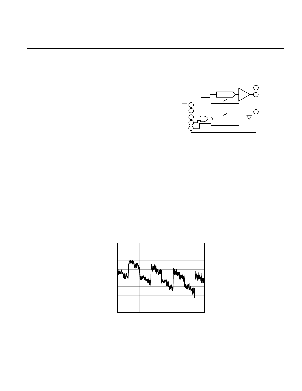
Complete 12-Bit DAC
DAC8512
FUNCTIONAL BLOCK DIAGRAM
Serial interface is high speed, three-wire, DSP compatible with
data in (SDI), clock (CLK) and load strobe (LD). There is also
a chip-select pin for connecting multiple DACs.
A CLR input sets the output to zero scale at power on or upon
user demand.
The DAC8512 is specified over the extended industrial (–40°C
to +85°C) temperature range. DAC8512s are available in plastic DIPs and SO-8 surface mount packages.
1.0
0.75
0.5
0.25
0
–0.25
LINEARITY ERROR – LSB
–0.5
–0.75
–1.0
0
DIGITAL INPUT CODE – Decimal
307220481024
4096
Linearity Error vs. Digital Input Code
REV. A
Information furnished by Analog Devices is believed to be accurate and
reliable. However, no responsibility is assumed by Analog Devices for its
use, nor for any infringements of patents or other rights of third parties
which may result from its use. No license is granted by implication or
otherwise under any patent or patent rights of Analog Devices.
One Technology Way, P.O. Box 9106, Norwood, MA 02062-9106, U.S.A.
Tel: 617/329-4700 World Wide Web Site: http://www.analog.com
Fax: 617/326-8703 © Analog Devices, Inc., 1996

DAC8512–SPECIFICATIONS
(@ V
ELECTRICAL CHARACTERISTICS
Parameter Symbol Condition Min Typ Max Units
STATIC PERFORMANCE
Resolution N Note 2 12 Bits
Relative Accuracy INL E Grade –1 ±1/4 +1 LSB
Differential Nonlinearity DNL No Missing Codes –1 ±3/4 +1 LSB
Zero-Scale Error V
Full-Scale Voltage V
Full-Scale Tempco TCV
ANALOG OUTPUT
Output Current I
Load Regulation at Full Scale L
Capacitive Load C
LOGIC INPUTS
Logic Input Low Voltage V
Logic Input High Voltage V
Input Leakage Current I
Input Capacitance C
INTERFACE TIMING SPECIFICATIONS
Clock Width High t
Clock Width Low t
Load Pulse Width t
Data Setup t
Data Hold t
Clear Pulse Width t
Load Setup t
Load Hold t
Select t
Deselect t
AC CHARACTERISTICS
4
Voltage Output Settling Time t
DAC Glitch 15 nV s
Digital Feedthrough 15 nV s
ZSE
FS
FS
OUT
REG
L
IL
IH
IL
IL
1, 4
CH
CL
LDW
DS
DH
CLRW
LD1
LD2
CSS
CSH
S
= +5.0 V 6 5%, –408C ≤ TA ≤ +858C, unless otherwise noted)
DD
F Grade –2 ±3/4 +2 LSB
Data = 000
Data = FFF
H
3
H
E Grade 4.087 4.095 4.103 V
+1/2 +3 LSB
F Grade 4.079 4.095 4.111 V
Notes 3, 4 16 ppm/°C
Data = 800
R
= 402 Ω to ∞, Data = 800
L
No Oscillation
H
4
H
±5 ±7mA
1 3 LSB
500 pF
0.8 V
2.4 V
10 µA
10 pF
30 10 ns
30 10 ns
20 ns
15 10 ns
15 5 ns
30 20 ns
15 ns
10 ns
30 ns
20 ns
To ±1 LSB of Final Value
5
16 µs
SUPPLY CHARACTERISTICS
Positive Supply Current I
Power Dissipation P
DD
DISS
VIH = 2.4 V, VIL = 0.8 V, No Load 1.5 2.5 mA
V
= 5 V, VIL = 0 V, No Load 0.5 1 mA
DD
VIH = 2.4 V, VIL = 0.8 V, No Load 7.5 12.5 mW
V
= 5 V, VIL = 0 V, No Load 2.5 5 mW
DD
Power Supply Sensitivity PSS ∆VDD = ±5% 0.002 0.004 %/%
NOTES
1
All input control signals are specified with tr = tf = 5 ns (10% to 90% of +5 V) and timed from a voltage level of 1.6 V.
2
1 LSB = 1 mV for 0 V to +4.095 V output range.
3
Includes internal voltage reference error.
4
These parameters are guaranteed by design and not subject to production testing.
5
The settling time specification does not apply for negative going transitions within the last 6 LSBs of ground. Some devices exhibit double the typical settling time in
this 6 LSB region.
Specifications subject to change without notice.
–2–
REV. A
DAC8512
WAFER TEST LIMITS
(@ VDD = +5.0 V 6 5%, TA = +258C, applies to part number DAC8512GBC only, unless otherwise noted)
Parameter Symbol Condition Min Typ Max Units
STATIC PERFORMANCE
Relative Accuracy INL –2 ± 3/4 +2 LSB
Differential Nonlinearity DNL No Missing Codes –1 ±0.7 +1 LSB
Zero-Scale Error V
Full-Scale Voltage V
ZSE
FS
Data = 000
Data = FFF
H
H
4.085 4.095 4.105 V
+1/2 +3 LSB
LOGIC INPUTS
Logic Input Low Voltage V
Logic Input High Voltage V
Input Leakage Current I
IL
IH
IL
2.4 V
0.8 V
10 µA
SUPPLY CHARACTERISTICS
Positive Supply Current I
Power Dissipation P
DD
DISS
VIH = 2.4 V, VIL= 0.8 V, No Load 1.5 2.5 mA
V
= 5 V, VIL = 0 V, No Load 0.5 1 mA
DD
VIH = 2.4 V, VIL = 0.8 V, No Load 7.5 12.5 mW
V
= 5 V, VIL = 0 V, No Load 2.5 5 mW
DD
Power Supply Sensitivity PSS ∆VDD = ±5% 0.002 0.004 %/%
NOTE
Electrical tests are performed at wafer probe to the limits shown. Due to variations in assembly methods and normal yield loss, yield after packaging is not guaranteed
for standard product dice. Consult factory to negotiate specifications based on dice lot qualifications through sample lot assembly and testing.
ABSOLUTE MAXIMUM RATINGS*
VDD to GND . . . . . . . . . . . . . . . . . . . . . . . . . . . –0.3 V, +10 V
Logic Inputs to GND . . . . . . . . . . . . . . . –0.3 V, V
V
to GND . . . . . . . . . . . . . . . . . . . . . –0.3 V, VDD + 0.3 V
OUT
I
Short Circuit to GND . . . . . . . . . . . . . . . . . . . . . . 50 mA
OUT
Package Power Dissipation . . . . . . . . . . . . . .(T
Thermal Resistance θ
JA
+ 0.3 V
DD
max – T
J
)/θ
A
8-Pin Plastic DIP Package (P) . . . . . . . . . . . . . . . . 103°C/W
8-Lead SOIC Package (S) . . . . . . . . . . . . . . . . . . . 158°C/W
Maximum Junction Temperature (T
max) . . . . . . . . . +150°C
J
Operating Temperature Range . . . . . . . . . . . . .–40°C to +85°C
Storage Temperature Range . . . . . . . . . . . . .–65°C to +150°C
Lead Temperature (Soldering, 10 secs) . . . . . . . . . . . . +300°C
*Stresses above those listed under “Absolute Maximum Ratings” may cause
permanent damage to the device. This is a stress rating only and functional
JA
operation of the device at these or any other conditions above those indicated in the
operational sections of this specification is not implied. Exposure to absolute
maximum rating conditions for extended periods may affect device reliability .
CAUTION
ESD (electrostatic discharge) sensitive device. Electrostatic charges as high as 4000 V readily
accumulate on the human body and test equipment and can discharge without detection.
Although the DAC8512 features proprietary ESD protection circuitry, permanent damage may
occur on devices subjected to high energy electrostatic discharges. Therefore, proper ESD
precautions are recommended to avoid performance degradation or loss of functionality.
ORDERING GUIDE
INL Temperature Package Package
Model (LSB) Range Description Option
DAC8512EP ±1 –40°C to +85°C 8-Pin P-DIP N-8
DAC8512FP ±2 –40°C to +85°C 8-Pin P-DIP N-8
DAC8512FS ±2 –40°C to +85° C 8-Lead SOIC SO-8
DAC8512GBC ±2 +25°C Dice
WARNING!
ESD SENSITIVE DEVICE
REV. A
–3–
DAC8512
SDI
CLK
CS
LD
SDI
CLK
LD
CLR
FS
V
OUT
ZS
D11 D10 D9 D8 D7 D6 D5 D3D4 D1D2 D0
t
css
t
ld1
t
t
ds
t
cl
dh
t
ch
t
ldw
t
s
±1 LSB
ERROR BAND
t
csh
t
ld2
t
clrw
t
S
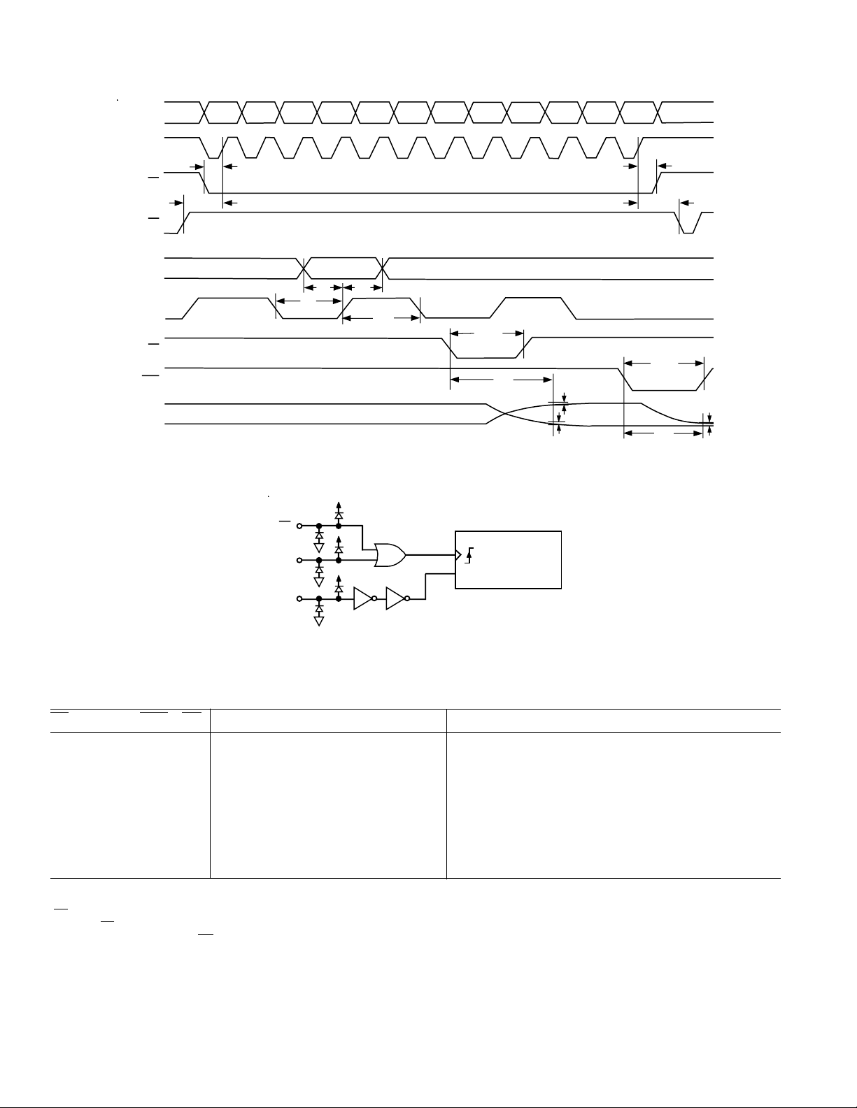
Figure 1. Timing Diagram
CS
ESD PROTECTION DIODES TO VDD AND GND
CLK
DATA
SDI
SHIFT
REGISTER
Figure 2. Equivalent Clock Input Logic
Table I. Control-Logic Truth Table
CS2CLK2CLR LD Serial Shift Register Function DAC Register Function
H X H H No Effect Latched
L L H H No Effect Latched
L H H H No Effect Latched
L ↑+ H H Shift-Register-Data Advanced One Bit Latched
↑+ L H H Shift-Register-Data Advanced One Bit Latched
HX H↓– No Effect Updated with Current Shift Register Contents
H X H L No Effect Transparent
H X L X No Effect Loaded with All Zeros
HX ↑+ H No Effect Latched All Zeros
NOTES
l
↑+ positive logic transition; ↓– negative logic transition; X = Don’t Care.
2
CS and CLK are interchangeable.
3
Returning CS HIGH avoids an additional “false clock” of serial data input.
4
Do not clock in serial data while LD is LOW.
–4–
REV. A
DAC8512
R1
R2
V
OUT
RAIL-TO-RAIL
OUTPUT
AMPLIFIER
R
BANDGAP
REFERENCE
2R
R
2R
2R
2R
SPDT
N-CH FET
SWITCHES
2R
AV = 4.095/2.5
= 1.638V/V
VOLTAGE SWITCHED 12-BIT
R-2R D/A CONVERTER
BUFFER
2.5V
PIN CONFIGURATIONS
SO-8 P-DIP-8 & Cerdip-8
V
CS
CLK
SDI
DD
1
DAC8512
2
TOP VIEW
3
(Not to Scale)
4
V
OUT
8
GND
7
CLR
6
LD
5
V
CS
CLK
SDI
DD
1
2
3
(Not to Scale)
4
DAC8512
TOP VIEW
8
V
OUT
GND
7
CLR
6
LD
5
PIN DESCRIPTIONS
Pin Name Description
1VDDPositive Supply. Nominal value +5 V, ± 5%.
CS Chip Select. Active low input.
2
3 CLK Clock input for the internal serial input shift register.
4 SDI Serial Data Input. Data on this pin is clocked into the
internal serial register on positive clock edges of the
CLK pin. The Most Significant Bit (MSB) is loaded
first.
LD Active low input which writes the serial register data
5
into the DAC register. Asynchronous input.
CLR Active low digital input that clears the DAC register to
6
zero, setting the DAC to minimum scale. Asynchronous
input.
7 GND Analog ground for the DAC. This also serves as the
digital logic ground reference voltage.
8V
Voltage output from the DAC. Fixed output voltage
OUT
range of 0 V to 4.095 V with 1 mV/LSB. An internal
temperature stabilized reference maintains a fixed
full-scale voltage independent of time, temperature and
power supply variations.
OPERATION
The DAC8512 is a complete ready to use 12-bit digital-to-analog
converter. It contains a voltage-switched, 12-bit, laser-trimmed
DAC, a curvature-corrected bandgap reference, a rail-to-rail
output op amp, a DAC register, and a serial data input register.
The serial data interface consists of a CLK, serial data in (SDI),
and a load strobe (
LD). This basic 3-wire interface offers maximum flexibility for interface to the widest variety of serial data
input loading requirements. In addition a
for multiple packaging loading and a power on reset
CS select is provided
CLR pin to
simplify start or periodic resets.
D/A CONVERTER SECTION
The DAC is a 12-bit voltage mode device with an output that
swings from GND potential to the 2.5 volt internal bandgap
voltage. It uses a laser trimmed R-2R ladder which is switched
by N channel MOSFETs. The output voltage of the DAC has a
constant resistance independent of digital input code. The DAC
output is internally connected to the rail-to-rail output op amp.
AMPLIFIER SECTION
The DAC’s output is buffered by a low power consumption precision amplifier. This amplifier contains a differential PNP pair
input stage which provides low offset voltage and low noise, as
well as the ability to amplify the zero-scale DAC output voltages. The rail-to-rail amplifier is configured in a gain of 1.6384
(= 4.095 V/2.5 V) in order to set the 4.095 volt full-scale output
(1 mV/LSB). See Figure 3 for an equivalent circuit schematic of
the analog section.
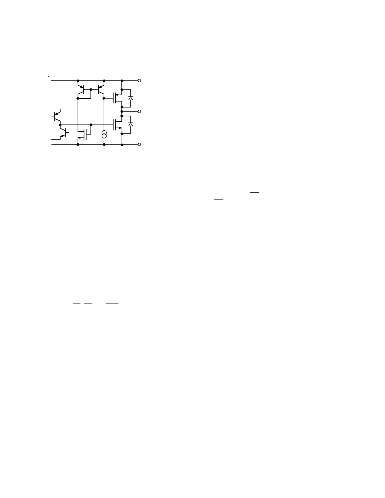
DICE CHARACTERISTICS
2
CS
3
CLK
SUBSTRATE IS COMMON WITH VDD.
NUMBER OF TRANSISTORS: 642
DIE SIZE: 0.055 inch × 0.106 inch; 5830 sq mils
V
DD
1
4
SDI LD
V
OUT
8
GND
7
GND
7
6
CLR
Figure 3. Equivalent DAC8512 Schematic of Analog
Portion
The op amp has a 16 µs typical settling time to 0.01%. There
are slight differences in settling time for negative slowing signals
5
vs. positive. See the oscilloscope photos in the typical performances section of this data sheet.
REV. A
–5–
DAC8512
OUTPUT SECTION
The rail-to-rail output stage of this amplifier has been designed
to provide precision performance while operating near either
power supply.
V
DD
P-CH
V
N-CH
OUT
AGND
Figure 4. Equivalent Analog Output Circuit
Figure 4 shows an equivalent output schematic of the rail-to-rail
amplifier with its N channel pull down FETs that will pull an
output load directly to GND. The output sourcing current is
provided by a P channel pull up device that can supply GND
terminated loads, especially at the low supply tolerance values of
4.75 volts. Figures 5 and 6 provide information on output swing
performance near ground and full-scale as a function of load. In
addition to resistive load driving capability the amplifier has also
been carefully designed and characterized for up to 500 pF capacitive load driving capability.
POWER SUPPLY
The very low power consumption of the DAC8512 is a direct
result of a circuit design optimizing use of the CBCMOS process. By using the low power characteristics of the CMOS for
the logic, and the low noise, tight matching of the complementary bipolar transistors good analog accuracy is achieved.
For power consumption sensitive applications it is important to
note that the internal power consumption of the DAC8512 is
strongly dependent on the actual logic input voltage levels
present on the SDI,
CS, LD, and CLR pins. Since these inputs
are standard CMOS logic structures they contribute static
power dissipation dependent on the actual driving logic V
V
voltage levels. The graph in Figure 9 shows the effect on to-
OL
OH
and
tal DAC8512 supply current as a function of the actual value of
input logic voltage. Consequently use of CMOS logic vs. TTL
minimizes power dissipation in the static state. A V
the SDI,
CS and CLR pins provides the lowest standby power
= 0 V on
IL
dissipation of 2.5 mW (500 µA × 5 V).
As with any analog system, it is recommended that the DAC8512
power supply be bypassed on the same PC card that contains the
chip. Figure 10 shows the power supply rejection versus frequency performance. This should be taken into account when using
higher frequency switched mode power supplies with ripple frequencies of 100 kHz and higher.
One advantage of the rail-to-rail output amplifier used in the
DAC8512 is the wide range of usable supply voltage. The part
is fully specified and tested over temperature for operation from
+4.75 V to +5.25 V. If reduced linearity and source current capability near full scale can be tolerated, operation of the DAC8512
is possible down to +4.3 volts. The minimum operating supply
voltage versus load current plot, in Figure 11, provides information for operation below V
TIMING AND CONTROL
= +4.75 V.
DD
The DAC8512 has a separate serial input register from the
12-bit DAC register that allows preloading of a new data value
into the serial register without disturbing the present DAC output voltage. After the new value is fully loaded in the serial input register it can be asynchronously transferred to the DAC
register by strobing the
sensitive
LD strobe that should be returned high before any
LD pin. The DAC register uses a level
new data is loaded into the serial input register. At any time the
contents of the DAC register can be reset to zero by strobing
the
CLR pin which causes the DAC output voltage to go to
zero volts. All of the timing requirements are detailed in Figure
1 along with the Table I Control-Logic Truth Table.
–6–
REV. A

5
80
–100
–60
–80
1
–20
–40
0
20
40
60
32
OUTPUT VOLTAGE – Volts
OUTPUT CURRENT – mA
POS0
CURRENT0
LIMIT0
NEG
CURRENT
LIMIT
DATA = 800
H
RL TIED TO +2V
10
90
100
0%
TIME = 20µs/DIV
20µs
1V
RL = NO LOAD
C
L
= 110pF
T
A
= +258C
1V/DIV
4
3
2
OUTPUT VOLTAGE – Volts
1
0
10
RL TIED TO +5V
DATA = 000H
100 100k10k1k
LOAD RESISTANCE – V
VDD = +5V
T
= +258C
A
RL TIED TO AGND
RL TIED TO AGND
D = FFFH
DATA = FFF
H
Typical Performance Characteristics — DAC8512
100
VDD = +5V
DATA = 000
10
TA = +858C
1
0.1
OUTPUT PULL-DOWN VOLTAGE – mV
0.01
1
H
TA = +258C
TA = –408C
10 1000100
OUTPUT SINK CURRENT – mA
Figure 5. Output Swing vs. Load
50mV
100
90
10
0%
OUTPUT NOISE VOLTAGE – 500µV/DIV
2mS
CODE = FFFH = 4095
BW = 630kHz
SCALE = 100X
TA = +258C
TIME = 2ms/DIV
10
Figure 8. Broadband Noise
5.0
∆VFS ≤ 1 LSB
4.8
DATA = FFF
TA = +258C
4.6
MIN – Volts
4.4
DD
V
4.2
4.0
0.01 0.1 101.0
H
PROPER OPERATION
WHEN V
VOLTAGE ABOVE
CURVE
0.04 0.4 4.0
OUTPUT LOAD CURRENT – mA
DD
SUPPLY
Figure 6. Pull-Down Voltage vs. Output Sink Current Capability
4.0
3.2
2.4
1.6
SUPPLY CURRENT – mA
0.8
0.0
0
LOGIC VOLTAGE VALUE – Volts
VDD = +5V
T
= +258C
A
NO LOAD
3241
5
Figure 9. Supply Current vs. Logic
Input Voltage
5
LD
0
– Volts
2.048
OUT
V
2.038
2.028
2.018
204810 TO 2047
TIME – 200ns/DIV
10
VDD = 5V
= +258C
T
A
Figure 7. Short Circuit Current
100
VDD = +5V 6200mV AC
= +258C
T
80
60
40
20
POWER SUPPLY REJECTION – dB
0
10
A
DATA = FFF
100 100k10k1k
FREQUENCY – Hz
H
Figure 10. Power Supply Rejection
vs. Frequency
Figure 11. Minimum Supply Voltage
vs. Load
REV. A
Figure 12. Midscale DAC Glitch
Figure 13. Large Signal Settling Time
Performance
–7–

DAC8512 — Typical Performance Characteristics
2.0
–2.0
4096
–1.0
–1.5
5120
0.0
–0.5
0.5
1.0
1.5
358430722560204815361024
DIGITAL INPUT CODE – Decimal
LINEARITY ERROR – LSB
VDD = +5V
T
A
= –408C, +258C, +858 C
+258 C & +858C
–408C
4
0
125
1
–25–50
2
3
1007550250
TEMPERATURE – 8C
SUPPLY CURRENT – mA
V
LOGIC
= 2.4V
DATA = FFF
H
NO LOAD
VDD = +4.75V
VDD = +5.25V
VDD = +5.0V
5
LD
0
16µs
1mV/DIV
OUTPUT VOLTAGE
TIME – 10µs/DIV
VDD = +5V
T
A
R
L
Figure 14. Rise Time Detail
60
50
40
30
20
NUMBER OF UNITS
10
0
0
–12
TOTAL UNADJUSTED ERROR – mV
TUE = ∑INL + ZS + FS
SS = 300 UNITS
TA = +25
= +258C
= NO LOAD
8
C
+12+40–4–8 +8
5
LD
0
1mV/DIV
OUTPUT VOLTAGE
TIME – 10µs/DIV
VDD = +5V
T
RL = NO LOAD
Figure 15. Fall Time Detail
4.115
4.110
4.105
AVG + 3σ
4.100
4.095
AVG
4.090
4.085
FULL-SCALE OUTPUT – Volts
4.080
4.075
AVG – 3σ
–25–50
VDD = +5V
NO LOAD
SS = 300 PCS
TEMPERATURE – 8C
= +258C
A
Figure 16. Linearity Error vs. Digital
Code
3
DATA = 000
NO LOAD
2
1
ZERO-SCALE – mV
0
125
1007550250
–1
–25–50
TEMPERATURE – 8C
V
DD
= +5.0V
1007550250
H
125
Figure 17. Total Unadjusted Error
Histogram
10
Hz
√
1
0.1
OUTPUT NOISE DENSITY – µV/
0.01
10
Figure 20. Output Voltage Noise vs.
Frequency
100 100k10k1k
FREQUENCY – Hz
VDD = +5V
T
= +258C
A
DATA = FFF
Figure 18. Full-Scale Voltage vs.
Temperature
5
4
H
3
2
1
0
–1
–2
–3
READINGS NORMALIZED
OUTPUT VOLTAGE CHANGE – mV
TO ZERO HOUR TIME POINT
–4
–5
200
0
HOURS OF OPERATION AT +1258C
135 UNITS TESTED
AVERAGE
1000600 800400
RANGE
1200
Figure 21. Long Term Drift Accelerated by Burn-In
–8–
Figure 19. Zero-Scale Voltage vs.
Temperature
Figure 22. Supply Current vs.
Temperature
REV. A
Typical Performance Characteristics—
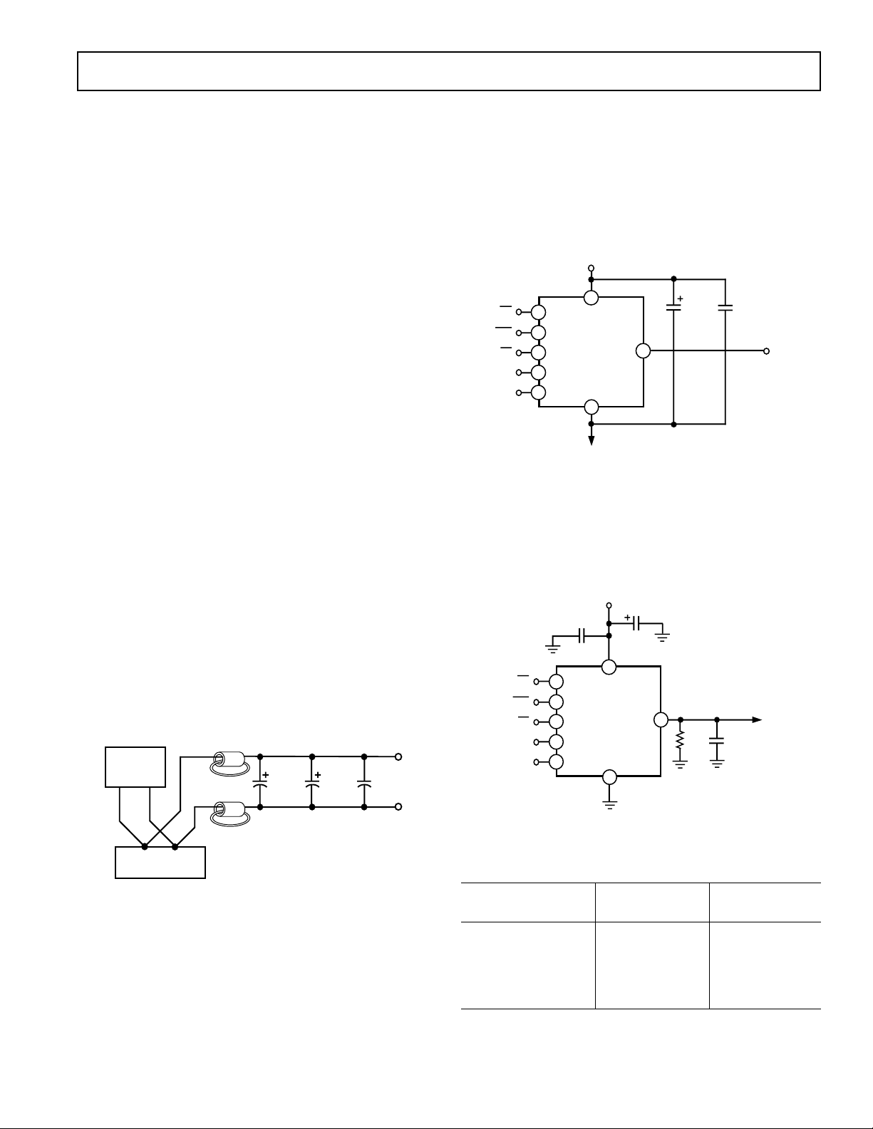
DAC8512
APPLICATIONS SECTION
Power Supplies, Bypassing, and Grounding
All precision converter products require careful application of
good grounding practices to maintain full rated performance.
Because the DAC8512 has been designed for +5 V applications,
it is ideal for those applications under microprocessor or microcomputer control. In these applications, digital noise is prevalent; therefore, special care must be taken to assure that its
inherent precision is maintained. This means that particularly
good engineering judgment should be exercised when addressing the power supply, grounding, and bypassing issues using the
DAC8512.
The power supply used for the DAC8512 should be well filtered
and regulated. The device has been completely characterized for
a +5 V supply with a tolerance of ± 5%. Since a +5 V logic supply is almost universally available, it is not recommended to
connect the DAC directly to an unfiltered logic supply without
careful filtering. Because it is convenient, a designer might be
inclined to tap a logic circuit’s supply for the DAC’s supply.
Unfortunately, this is not wise because fast logic with nanosecond transition edges induce high current pulses. The high transient current pulses can generate glitches hundreds of millivolts
in amplitude due to wiring resistances and inductances. This
high frequency noise will corrupt the analog circuits internal to
the DAC and cause errors. Even though their spike noise is
lower in amplitude, directly tapping the output of a +5 V system
supply can cause errors because these supplies are of the switching regulator type that can and do generate a great deal of high
frequency noise. Therefore, the DAC and any associated analog
circuitry should be powered directly from the system power supply outputs using appropriate filtering. Figure 23 illustrates how
a clean, analog-grade supply can be generated from a +5 V logic
supply using a differential LC filter with separate power supply
and return lines. With the values shown, this filter can easily
handle 100 mA of load current without saturating the ferrite
cores. Higher current capacity can be achieved with larger ferrite
cores. For lowest noise, all electrolytic capacitors should be low
ESR (Equivalent Series Resistance) type.
FERRITE BEADS:
TTL/CMOS
LOGIC
CIRCUITS
2 TURNS, FAIR-RITE
#2677006301
100µF
ELECT
.
10-22µF
TANT.
+5V
0.1µF
CER.
+5V
RETURN
the ground connection of the DAC8512 be connected to a high
quality analog ground, such as the one described above. Generous bypassing of the DAC’s supply goes a long way in reducing
supply line-induced errors. Local supply bypassing consisting of
a 10 µF tantalum electrolytic in parallel with a 0.1 µF ceramic is
recommended. The decoupling capacitors should be connected
between the DAC’s supply pin (Pin 1) and the analog ground
(Pin 7). Figure 24 shows how the ground and bypass connections should be made to the DAC8512.
+5V
CS
CLR
SCLK
SDI
1
2
6
5
LD
3
4
V
DD
DAC8512
GND
7
TO ANALOG GROUND
V
8
OUT
10µF
0.1µF
V
OUT
Figure 24. Recommended Grounding and Bypassing
Scheme for the DAC8512
Unipolar Output Operation
This is the basic mode of operation for the DAC8512. As shown
in Figure 24, the DAC8512 has been designed to drive loads as
low as 2 kΩ in parallel with 500 pF. The code table for this operation is shown in Table II.
+5V
1
V
DD
GND
7
10µF
V
OUT
0V ≤ V
≤ 4.095V
8
2kΩ
OUT
500pF
CLR
SCLK
SDI
0.1µF
CS
2
6
DAC8512
5
LD
3
4
Figure 25. Unipolar Output Operation
+5V
POWER SUPPLY
Figure 23. Properly Filtering a +5 V Logic Supply Can Yield
a High Quality Analog Supply
In order to fit the DAC8512 in an 8-pin package, it was necessary to use only one ground connection to the device. The
ground connection of the DAC serves as the return path for
supply currents as well as the reference point for the digital input thresholds. The ground connection also serves as the supply
rail for the internal voltage reference and the output amplifier.
Therefore, to minimize any errors, it is recommended that
REV. A
–9–
Table II. Unipolar Code Table
Hexadecimal Number Decimal Number Analog Output
in DAC Register in DAC Register Voltage (V)
FFF 4095 +4.095
801 2049 +2.049
800 2048 +2.048
7FF 2047 +2.047
000 0 0

DAC8512
+5V
10µF
+
0.1µF
1
8
7
4
3
2
5
6
DAC8512
V
DD
GND
R1
10kΩ
R2
12.7k
R3
247kΩ
6
5
4
8
7
–5V ≤ V
O
≤ +5V
+5V
–5V
A2
P2
10kΩ
ZERO SCALE
ADJUST
P3
500Ω
R4
23.7kΩ
FULL SCALE
ADJUST
–2.5V
CLR
LD
CS
SCLK
SDI
0.1µF
+5V
REF03
A1
–2.5V
0.01µF
100Ω
P1
10kΩ
2.5V
TRIM
2
6
5
4
2
1
3
A1, A2 = 1/2 OP295
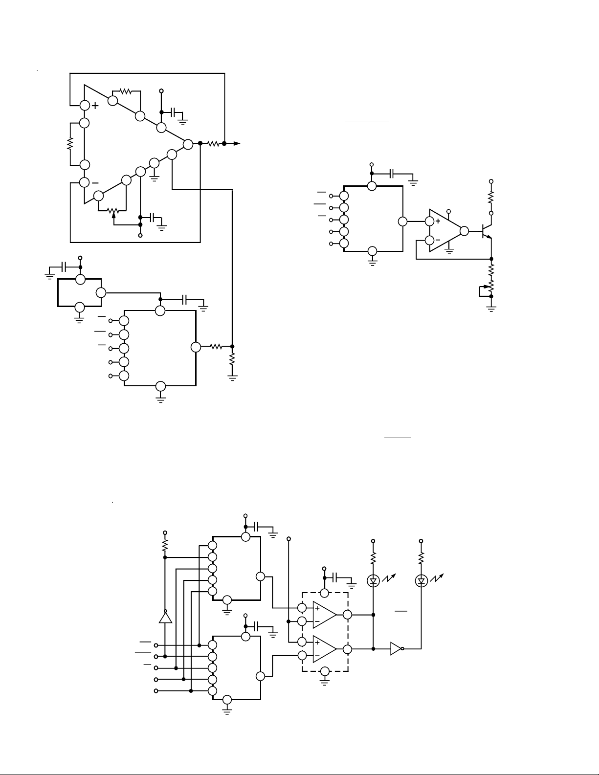
Operating the DAC8512 on +12 V or +15 V Supplies Only
Although the DAC8512 has been specified to operate on a
single, +5 V supply, a single +5 V supply may not be available in
many applications. Since the DAC8512 consumes no more than
2.5 mA, maximum, then an integrated voltage reference, such as
the REF02, can be used as the DAC8512 +5 V supply. The
configuration of the circuit is shown in Figure 26. Notice that
the reference’s output voltage requires no trimming because of
the REF02’s excellent load regulation and tight initial output
voltage tolerance. Although the maximum supply current of the
DAC8512 is 2.5 mA, local bypassing of the REF02’s output
with at least 0.1 µF at the DAC’s voltage supply pin is recom-
mended to prevent the DAC’s internal digital circuits from affecting the DAC’s internal voltage reference.
+12V OR +15V
2
REF02
4
0.1µF
SCLK
6
CS
CLR
LD
SDI
2
6
5
3
4
1
V
DD
DAC8512
GND
7
0.1µF
8
V
OUT
By adding a pull-down resistor from the output of the DAC8412
to a negative supply as shown in Figure 27, offset errors can
now be read at zero code. This configuration forces the output
p-channel MOSFET to source current to the negative supply
thereby allowing the designer to determine in which direction the
offset error appears. The value of the resistor should be such that,
at zero code, current through the resistor is 200 µA, maximum.
Bipolar Output Operation
Although the DAC8512 has been designed for single-supply operation, bipolar operation is achievable using the circuit illustrated in Figure 28. The circuit uses a single-supply, rail-to-rail
OP295 op amp and the REF03 to generate the –2.5 V reference
required to level-shift the DAC output voltage. Note that the –
2.5 V reference was generated without the use of precision resistors. The circuit has been configured to provide an output
voltage in the range –5 V ≤ V
≤ +5 V and is coded in com-
OUT
plementary offset binary. Although each DAC LSB corresponds
to 1 mV, each output LSB has been scaled to 2.44 mV. Table
III provides the relationship between the digital codes and output voltage.
The transfer function of the circuit is given by:
V
= –1 mV × Digital Code ×
O
R4
R1
+ 2.5 ×
R4
R2
and, for the circuit values shown, becomes:
= –2.44 mV × Digital Code + 5 V
V
O
Figure 26. Operating the DAC8512 on +12 V or +15 V
Supplies Using a REF02 Voltage Reference
Measuring Offset Error
One of the most commonly specified endpoint errors associated
with real world nonideal DACs is offset error.
In most DAC testing, the offset error is measured by applying
the zero-scale code and measuring the output deviation from 0
volt. There are some DACs where offset errors may be present
but not observable at the zero scale because of other circuit limitations (for example, zero coinciding with single-supply ground).
In these DACs, nonzero output at zero code cannot be read as
the offset error. In the DAC8512, for example, the zero-scale
error is specified to be ±3 LSBs. Since zero scale coincides with
zero volt, it is not possible to measure negative offset error.
Figure 27. Measuring Zero-Scale or Offset Error
CS
2
6
CLR
5
LD
SDI
3
4
SCLK
SET CODE = 000
+5V
0.1µF
1
V
DD
DAC8512
GND
7
AND MEASURE V
H
8
OUT
R
V–
200µA, MAX
V
OUT
–10–
Figure 28. Bipolar Output Operation
REV. A

DAC8512
910
6
11 12
14 15
7
3254
R2
5.1kΩ
R1
510kΩ
C1
0.02µF
C2
47µF
D1
1N4001C347µF
1N5231
5.1V
ZENER
D2
1N4001
R3
470Ω
–5V
INVERTERS = CD4049
Table III. Bipolar Code Table
Hexadecimal Number Decimal Number Analog Output
in DAC Register in DAC Register Voltage (V)
F
FF 4095 –4.9976
801 2049 –2.44E–3
800 2048 0
7FF 2047 +2.44E–3
000 0 +5
To maintain monotonicity and accuracy, R1, R2, and R4 should
be selected to match within 0.01% and must all be of the same
(preferably metal foil) type to assure temperature coefficient
matching. Mismatching between R1 and R2 causes offset and gain
errors while an R4 to R1 and R2 mismatch yields gain errors.
For applications that do not require high accuracy, the circuit
illustrated in Figure 29 can also be used to generate a bipolar
output voltage. In this circuit, only one op amp is used and no
potentiometers are used for offset and gain trim. The output
voltage is coded in offset binary and is given by:
V
= 1 mV × Digital Code ×
O
R2
–2.5
×
R1
R4
R3+R4
×
R2
1+
R1
Generating a Negative Supply Voltage
Some applications may require bipolar output configuration but
only have a single power supply rail available. This is very common in data acquisition systems using microprocessor-based
systems. In these systems, +12 V, +15 V, and/or +5 V are only
available. Shown in Figure 30 is a method of generating a negative supply voltage using one CD4049, a CMOS hex inverter,
operating on +12 V or +15 V. The circuit is essentially a charge
pump where two of the six are used as an oscillator. For the values shown, the frequency of oscillation is approximately 3.5 kHz
and is fairly insensitive to supply voltage because R1 > 2 × R2.
The remaining four inverters are wired in parallel for higher output current. The square wave output is level translated by C2 to
a negative-going signal, rectified using a pair of 1N4001s, and
then filtered by C3. With the values shown, the charge pump
will provide an output voltage of –5 V for current loadings in the
range 0.5 mA ≤ I
≤ I
≤ 7 mA with a +12 V supply.
OUT
≤ 10 mA with a +15 V supply and 0.5 mA
OUT
Figure 29. Bipolar Output Operation without Trim
For the ±2.5 V output range and the circuit values shown in the
table, the transfer equation becomes:
Similarly, for the ±5 V output range, the transfer equation
becomes:
REV. A
+5V
REF03
CS
2
CLR
6
LD
5
SDI
3
4
V
O
SCLK
VO = 2.44 mV × Digital Code – 5 V
0.1µF
2
6
4
+5V
1
V
DD
DAC8512
GND
7
+2.5V
0.1µF
R1
R3
8
V
OUT
R2
2
A1
3
A1 = 1/2 OP295
R4
R1
RANGE R2
65V
10k
10k
62.5V
+5V
–5V
8
10k
20k
1
4
R3
10k
10k
= 1.22 mV × Digital Code – 2.5 V
V
R4
15.4k + 274
43.2k + 499
Figure 30. Generating a –5 V Supply When Only +12 V
or +15 V Is Available
A High-Compliance, Digitally Controlled Precision Current
Source
The circuit in Figure 31 shows the DAC8512 controlling a
high-compliance precision current source using an AMP05 in-
O
strumentation amplifier. The AMP05’s reference pin becomes
the input, and the “old” inputs now monitor the voltage across a
precision current sense resistor, R
. Voltage gain is set to unity,
CS
so the transfer function is given by the following equation:
V
IN
=
I
OUT
R
CS
If R
equals 100 Ω, the output current is limited to +10 mA
CS
with a 1 V input. Therefore, each DAC LSB corresponds to
2.4 µA. If a bipolar output current is required, then the circuit
in Figure 28 can be modified to drive the AMP05’s reference
pin with a ±1 V input signal.
Potentiometer P1 trims the output current to zero with the input at 0 V. Fine gain adjustment can be accomplished by adjusting R1 or R2.
–11–
DAC8512
FULL-SCALE
ADJUST
A1 = 1/2 OP295
+5V
6
2
8
DAC8512FP
1
CS
CLR
5
3
4
LD
SCLK
SDI
7
3
2
A1
1
+5V
0.1µF
V
S
LOAD
2N2222
R1
4.02kΩ
P1
200Ω
100k
0.1µF
R1
REF02
+15V
4
R2
5kΩ
17
18
7
AMP05
1
4
CS
SDI
6
LD
P1
100kΩ
5
–15V
2
6
5
3
4
2
2
CLR
SCLK
+15V
0.1µF
6
12
8
9
11
0.1µF
1
DAC8512FZ
7
0.1µF
R
CS
100Ω
10
0mA ≤ I
OUT
2.4µA/ BIT
R3
3k
8
R4
1k
Figure 31. A High-Compliance, Digitally Controlled
Precision Current Source
A Single-Supply, Programmable Current Source
The circuit in Figure 32 shows how the DAC8512 can be used
with an OP295 single-supply, rail-to-rail output op amp to provide a digitally programmable current sink from V
SOURCE
consumes less than 3.8 mA, maximum. The DAC’s output voltage is applied across R1 by placing the 2N2222 transistor in the
+5V
+5V
1
DAC8512
7
+5V
1
DAC8512
7
6
2
5
3
4
6
2
5
3
4
1kΩ
2
1/6
74HC05
CLR
HDAC/LDAC
LD
SCLK
SDI
1
Figure 33. A Digitally Programmable Window Detector
≤ 10mA
that
0.1µF
8
0.1µF
8
OP295’s feedback loop. For the circuit values shown, the fullscale output current is 1 mA which is given by the following
equation:
OUT
DW × 4.095V
=
R1
I
where DW = DAC8512’s binary digital input code.
Figure 32. A Single-Supply, Programmable Current
Source
The usable output voltage range of the current sink is +5 V to
+60 V. The low limit of the range is controlled by transistor
saturation, and the high limit is controlled by the collector-base
breakdown voltage of the 2N2222.
A Digitally Programmable Window Detector
A digitally programmable, upper/lower limit detector using two
DAC8512s is shown in Figure 33. The required upper and
lower limits for the test are loaded into each DAC individually
by controlling HDAC/
LDAC. If a signal at the test input is not
within the programmed limits, the output will indicate a logic
zero which will turn the red LED on.
V
IN
+5V
3
5
C1
4
7
C2
6
12
C1, C2 = 1/4 CMP-404
0.1µF
2
1
+5V
R1
604Ω
RED LED
PASS/FAIL
+5V
T1
34
1/6
74HC05
R2
604Ω
GREEN LED
T1
–12–
REV. A
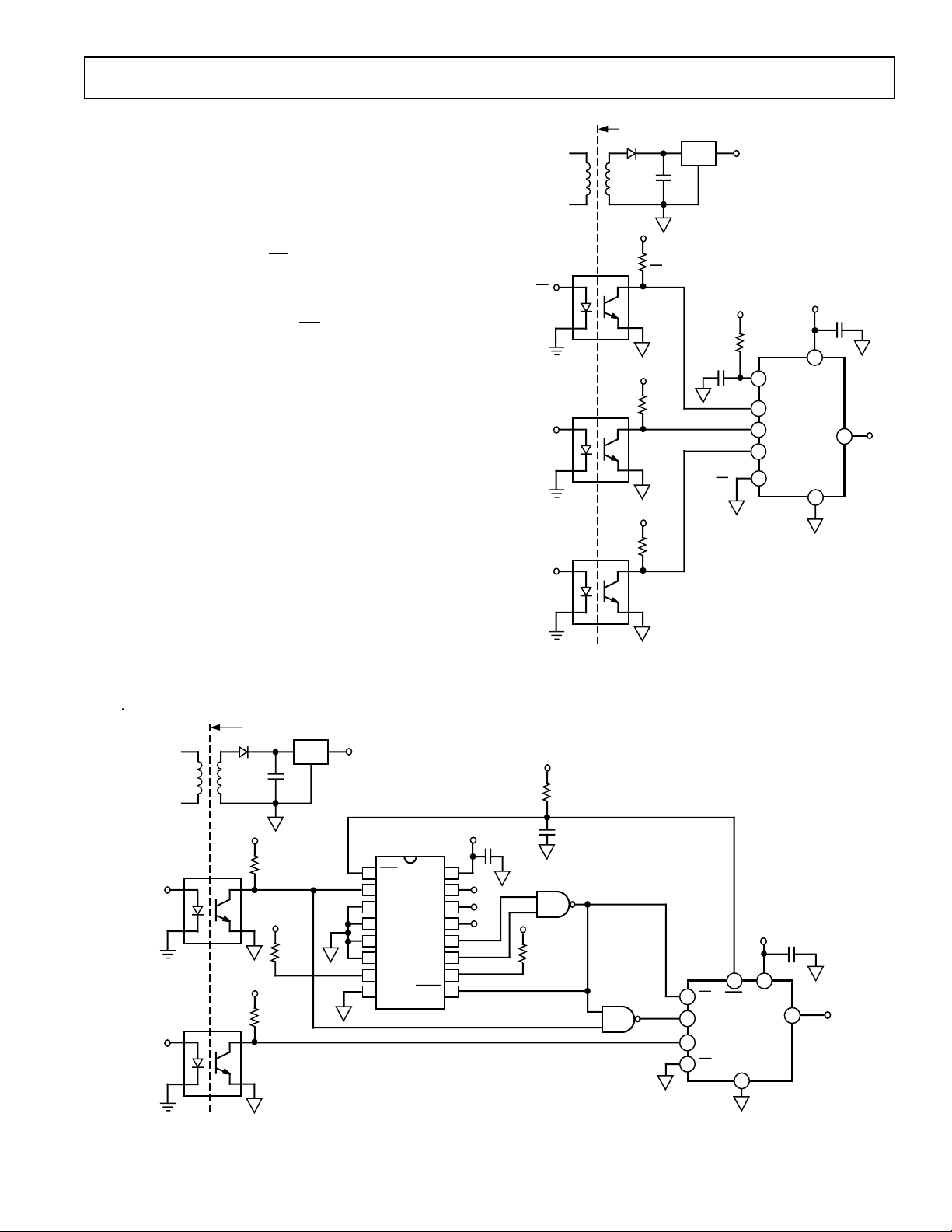
Opto-Isolated Interfaces for Process Control Environments
0.1µF
+5V
5
6
8
DAC8512
1
CS
3
4
7
2
0.1µF
10kΩ
+5V
V
OUT
+5V
+5V
+5V
10kΩ
SCLK
10kΩ
SDI
10kΩ
LD
LD
SCLK
SDI
+5V
REG
+5V
POWER
HIGH VOLTAGE
ISOLATION
In many process control type applications, it is necessary to provide an isolation barrier between the controller and the unit being controlled. Opto-isolators can provide isolation in excess of
3 kV. The serial loading structure of the DAC8512 makes it
ideal for opto-isolated interfaces as the number of interface lines
is kept to a minimum.
Illustrated in Figure 34 is an opto-isolated interface using the
DAC8512. In this circuit, the
CS line is always LOW to enable
the DAC, and the 10 kΩ/1 µF combination connected to the
DAC’s
CLR pin sets a turn-on time constant of 10 ms to reset
the DAC upon application of power. Three opto-couplers are
then used for the SDI, SCLK, and
LD lines.
Often times reducing the number of interface lines to two lines
is required in many control environments. The circuit illustrated
in Figure 35 shows how to convert a two-line interface into the
three control lines required to control the DAC8512 without using one shots. This technique uses a counter to keep track of the
clock cycles and, when all the data has been input to the DAC,
the external logic generates the
LD pulse.
DAC8512
POWER
SCLK
SDI
HIGH VOLTAGE
ISOLATION
+5V
+5V
10kΩ
+5V
10kΩ
10kΩ
+5V
REG
Figure 34. An Opto-Isolated DAC Interface
+5V
+5V
74HC161
1
2
3
4
5
6
7
8
CLR
CLK
A
B
C
D
ENP
GND
V
RCO
ENT
LOAD
16
CC
15
NC
Q
14
NC
A
13
Q
Q
Q
NC
B
12
C
11
D
10
9
0.1µF
+5V
10kΩ
1µF
1/4 74HCOO
1
X
2
+5V
10kΩ
3
1/4 74HCOO
4
Y
5
+5V
0.1µF
1
6
5
6
LD
3
SCLK
SDI
4
2
CS
V
CLR
DD
DAC8512
GND
7
8
V
OUT
REV. A
Figure 35. A Two-Wire, Opto-lsolated DAC Interface
–13–

DAC8512
V
OUT3
DAC8512
#3
V
OUT2
DAC8512
#2
V
OUT1
DAC8512
#1
8
4
5
2
3
6
V
CC
1G
1A
1B
2G
2A
2B
GND
1Y0
1Y1
1Y2
1Y3
2Y0
2Y1
2Y2
2Y3
12
1kΩ
+5V
16
1
2
3
15
14
13
8
11
10
9
7
6
5
4
NC
NC
NC
NC
+5V
ENABLE
CODED
ADDRESS
C1
0.1µF
74HC139
V
OUT4
DAC8512
#4
+5V
R1
1k
SCLK
SDI
LD
8
4
5
2
3
6
8
4
5
2
3
6
8
4
5
2
3
6
COUNTER
CLK
Q
D
Q
C
Q
B
Q
A
LOAD
(X)
DAC8512
CLK (Y)
LOAD = QC · Q
DAC8512 CLK = LOAD · SCLK
LOAD DAC
D
Figure 36. Opto-lsolated Two-Wire Serial Interface Timing Diagram
The timing diagram of Figure 36 can be used to understand the
operation of the circuit. Only two opto-couplers are used in the
circuit; one for SCLK and one for SDI. The 74HC161 counter
in incremented on every rising edge of the clock. Additionally,
the data is loaded into the DAC8512 on the falling edge of the
clock by inverting the serial clock using gate “Y.” The timing
diagram shows that after the twelfth bit has been clocked the
output of the counter is binary 1011. On the very next rising
clock edge, the output of the counter changes to binary 1100
upon which the output of gate “X” goes LOW to generate the
LD pulse. The LD signal is connected to both the DAC’s LD
and the counter’s LOAD pins to prevent the thirteenth rising
clock edge from advancing the DAC’s internal shift register.
This prevents false loading of data into the DAC8512. Inverting
the DAC’s serial clock allows sufficient time from the CLK edge
to the
LD edge, and from the LD edge to the next clock pulse
all of which satisfies the timing requirements for loading the
DAC8512.
After loading one address of the DAC, the entire process can repeated to load another address. If the loading is complete, then
the clock must stop after the thirteenth pulse of the final load.
The DAC’s clock input will be pulled high and the counter reset
to zero. As was shown in Figure 35, both the 74HC161’s and
the DAC8512’s
CLR pins are connected to a simple R-C timing
circuit that resets both ICs when the power in turned on. The
circuit’s time constant should be set longer than the power supply turn-on time and, in this circuit, is set to 10 ms, which
should be adequate for most systems. This same two-wire interface can be used for other three-wire serial input DACs.
Decoding Multiple DAC8512s
The CS function of the DAC8512 can be used in applications
to decode a number of DACs. In this application, all DACs receive the same input data; however, only one of the DAC’s
input is asserted to transfer its serial input register contents into
the destination DAC register. In this circuit, shown in Figure 37,
the
CS timing is generated by a 74HC139 decoder and should
follow the DAC8512’s standard timing requirements. To prevent timing errors, the 74HC139 should not be activated by its
CS
–14–
ENABLE input while the coded address inputs are changing. A
simple timing circuit, R1 and C1, connected to the DACs’
CLR
pins resets all DAC outputs to zero during power-up.
Figure 37. Decoding Multiple DAC8512s Using the CS Pin
REV. A

CS
CLR
LD
SCLK
SDI
V
+625mV
IN
R1
619Ω
0.1µF
2
6
5
DAC8512FZ
3
4
R2
4.32kΩ
DAC8512
V+
AD600JN
1
2
3
4
5
6
7
8
V+
1
7
REF
8
16
15
14
13
12
11
10
9
R6
2.26kΩ
1µF
0.1µF
V+
V–
0.1µF
R3
402Ω
R4
402Ω
0 ≤ VG ≤ 1.25V
R7
1kΩ
R5
806Ω
V+
0.1µF
2
AD844
3
6
0.1µF
V–
R4
49.9Ω
SUPPLY DECOUPLING NETWORK
+5V
10µF
FB = FAIR RITE
V+
V–
#2743001111
10µF
–5V
V
OUT
0.01dB/BIT
Figure 38. A Digitally Controlled, Ultralow Noise VCA
A Digitally Controlled, Ultralow Noise VCA
The circuit in Figure 38 illustrates how the DAC8512 can be
used to control an ultralow noise VCA, using the AD600/
AD602. The AD600/AD602 is a dual, low noise, wideband,
variable gain amplifier based on the X-AMP topology.* Both
channels of the AD600 are wired in parallel to achieve a
wideband VCA which exhibits an RTI (Referred To Input)
noise voltage spectral density of approximately 1 nV/√
Hz. The
output of the VCA requires an AD844 configured in a gain of 4
to account for signal loss due to input and output 50 Ω terminations. As configured, the total gain in the circuit is 40 dB.
Since the output of the DAC8512 is single quadrant, it was necessary to offset the AD600’s gain control voltage so that the gain
of the circuit is 0 dB for zero scale and 40 dB at full scale. This
was achieved by setting C1LO and C2LO to +625 mV using R1
and R2. Next, the output of the DAC8512 was scaled so that
the gain of the AD600 equaled 20 dB when the digital input
code equaled 800
. The frequency response of the VCA as a
H
function of digital code is shown in Figure 39.
+70
+60
+50
+40
+30
+20
+10
SYSTEM GAIN – dB
–10
–20
–30
4095
3072
2048
1024
0
0
100k 100M10M1M10k
FREQUENCY – Hz
Figure 39. VCA Frequency Response vs. Digital Code
*For more details regarding the AD600 or AD602, please consult the AD600/
AD602 data sheet.
REV. A
–15–

DAC8512
A Serial DAC, Audio Volume Control
The DAC8512 is well suited to control digitally the gain or attenuation of a voltage controlled amplifier. In professional audio
mixing consoles, music synthesizers, and other audio processors,
VCAs, such as the SSM2018, adjust audio channel gain and attenuation from front panel potentiometers. The VCA provides a
clean gain transition control of the audio level when the slew
rate of the analog input control voltage, V
, is properly chosen.
C
The circuit in Figure 40 illustrates a volume control application
using the DAC8512 to control the attenuation of the SSM2018.
+15V
10MΩ
P1
100kΩ
OFFSET
TRIM
+15V
V
0.1µF
REF02
IN
+15V
–15V
0.1µF
2
4
18kΩ
CS
CLR
LD
6
2
6
5
3SCLK
4SDI
500kΩ
P2
SYMMETRY
TRIM
1
2
3
4
5
6
7
8
47pF
+5V
1
DAC8512
7
470kΩ
10pF
18kΩ
16
15
14
SSM2018
0.1µF
13
12
11
10
9
R6
825Ω
8
1kΩ
* – PRECISION RESISTOR
PT146
1kΩ COMPENSATOR
30kΩ
0.1µF
0V ≤ VC ≤ +2.24V
R7
*
C
1µF
V
+15V
–15V
CON
OUT
Figure 40. A Serial DAC, Audio Volume Control
Since the supply voltage available in these systems is typically
±15 V or ±18 V, a REF02 is used to supply the +5 V required
to power the DAC. No trimming of the reference is required because of the reference’s tight initial tolerance and low supply
current consumption of the DAC8512. The SSM2018 is configured as a unity-gain buffer when its control voltage equals 0
volt. This corresponds to a 000
code from the DAC8512.
H
Since the SSM2018 exhibits a gain constant of –28 mV/dB
(typical), the DAC’s full-scale output voltage has to be scaled
down by R6 and R7 to provide 80 dB of attenuation when the
Table IV. SSM-2018 VCA Attenuation vs.
DAC8512 Input Code
Hexadecimal Number Control VCA
in DAC Register Voltage (V) Attenuation (dB)
000 0 0
400 +0.56 20
800 +1.12 40
C00 +1.68 60
FFF +2.24 80
digital code equals FFFH. Therefore, every DAC LSB corresponds to 0.02 dB of attenuation. Table IV illustrates the attenuation vs. digital code of the volume control circuit.
To compensate for the SSM2018’s gain constant temperature
coefficient of –3300 ppm/°C, a 1 kΩ, temperature-sensitive resistor (R7) manufactured by the Precision Resistor Company
with a temperature coefficient of +3500 ppm/°C is used. A
C
of 1 µF provides a control transition time of 1 ms which
CON
yields a click-free change in the audio channel attenuation. Symmetry and offset trimming details of the VCA can be found in
the SSM2018 data sheet.
Information regarding the PT146 1 kΩ “Compensator” can be
obtained by contacting:
Precision Resistor Company, Incorporated
10601 75th Street North
Largo, Fl 34647
(813) 541-5771
An Isolated, Programmable, 4-20 mA Process Controller
In many process control system, applications, two-wire current
transmitters are used to transmit analog signals through noisy
environments. These current transmitters use a “zero-scale” signal current of 4 mA that can be used to power the transmitter’s
signal conditioning circuitry. The “full-scale” output signal in
these transmitters is 20 mA. The converse approach to process
control can also be used; a low-power, programmable current
source can be used to control remotely located sensors or devices in the loop.
A circuit that performs this function is illustrated in Figure 41.
Using the DAC8512 as the controller, the circuit provides a
programmable output current of 4 mA to 20 mA, proportional
to the DAC’s digital code. Biasing for the controller is provided
by the REF02 and requires no external trim for two reasons:
(1) the REF02’s tight initial output voltage tolerance and (2) the
low supply current consumption of both the OP90 and the
DAC8512. The entire circuit, including opto-couplers, consumes less than 3 mA from the total budget of 4 mA. The OP90
regulates the output current to satisfy the current summation at
the noninverting node of the OP-90. The KCL equation at
Pin 3 is given by:
–16–
I
OUT
=
1
1 mV ×Digital Code ×R3
×
R7
R1
+
R2
×R3
V
REF
REV. A

DAC8512
PC1
PC0
SCK
MOSI
SS
CLK
SDI
LD
MC68HC11* DAC8512*
CS
CLR
*ADDITIONAL PINS OMITTED FOR CLARITY
R2
976kΩ
P2
P1
10kΩ
20mA
80.6k
R3
10kΩ
ILQ-1
50Ω
4mA
ADJUST
D1
R4
54.9k
D1 = HP5082-2810
+5V
CLR
LD
SCLK
SCI
6
5
DAC8512
3
4
1
R1
200kΩ
8
7
CLK
ADJUST
360Ω
Figure 41. An Isolated, Programmable, 4-20 mA Process Controller
For the values shown in Figure 41,
= 3.9 µA × Digital Code + 4 mA
I
OUT
giving a full-scale output current of 20 mA when the
DAC8512’s digital code equals FFF
. Offset trim at 4 mA is
H
provided by P2, and P1 provides the circuit’s gain trim at 20 mA.
These two trims do not interact because the noninverting input
of the OP90 is at virtual ground. The Schottky diode, D1, is required in this circuit to prevent loop supply power-on transients
from pulling the noninverting input of the OP90 more than
300 mV below its inverting input. Without this diode, such transients could cause phase reversal of the OP90 and possible
latchup of the controller. The loop supply voltage compliance of
the circuit is limited by the maximum applied input voltage to
the REF02 and is from +12 V to +40 V.
MICROPROCESSOR INTERFACING
DAC8512–MC68HC11 Interface
The circuit illustrated in Figure 42 shows a serial interface between the DAC8512 and the MC68HC11 8-bit microcontroller. SCK of the 68HC11 drives SCLK of the DAC8512, while
the MOSI output drives the serial data line, SDI, of the
DAC8512. The DAC’s
CLR, LD, and CS signals are derived
from port lines PC1, PD5, and PC0, respectively, as shown.
For correct operation of the serial interface, the 68HC11 should
be configured such that its CPOL bit is set to 1 and its CPHA
bit is also set to 1. When the serial data is to be transmitted to
the DAC, PC0 is taken low, asserting the DAC’s
CS input.
When the 68HC11 is configured in this manner, serial data on
3
2
6
7
6
OP90
4
SCLK
REPEAT FOR SDI, LD, & CLR
REF02
4
150Ω
R6
R5
100k
2
R7
100Ω
Q1
2N1711
4–20mA
V
LOOP
+12 TO +40V
R
L
100Ω
Figure 42. DAC8512–MC68HC11 Interface
MOSI is valid on the rising edge of SCLK. The 68HC11 transmits its serial data in 8-bit bytes (MSB first), with only eight rising clock edges occurring in the transmit cycle. To load data to
the DAC8512’s input serial register, PC0 is left low after the
first eight bits are transferred, and a second byte of data is then
transferred serially to the DAC8512. During the second byte
load, the first four most significant bits of the first byte are
pushed out of the DAC’s input shift register. At the end of the
second byte load, PC0 is then taken high. To prevent an accidental advancing of the internal shift register, SCLK must already be asserted before PC0 is taken high. To transfer the
contents of the input shift register to the DAC register, PD5 is
taken low, asserting the DAC’s
LD input. The DAC’s CLR input, controlled by the 68HC11’s PC1 port, provides an asynchronous clear function, setting the DAC output to zero.
Included in this section is the source code for operating the
DAC8512—M68HC11 interface.
REV. A
–17–

DAC8512
DAC8512–M68HC11 Interface Program Source Code
*
PORTC EQU $1003 Port C control register
* “0,0,0,0;0,0,CLR/,CS/”
DDRC EQU $1007 Port C data direction
PORTD EQU $1008 Port D data register
* “0,0,LD/,SCLK;SDI,0,0,0
DDRD EQU $1009 Port D data direction
SPCR EQU $1028 SPI control register
* “SPIE,SPE,DWOM,MSTR;CPOL,CPHA,SPRl,SPR0”
SPSR EQU $1029 SPI status register
* “SPIF,WCOL,0,MODF;0,0,0,0”
SPDR EQU $102A SPI data register; Read-Buffer; Write-Shifter
*
* SDI RAM variables: SDI1 is encoded from 0 (Hex) to F (Hex)
* SDI2 is encoded from 00 (Hex) to FF (Hex)
* DAC requires two 8-bit loads; upper 4 bits of SDI1
* are ignored.
*
SDI1 EQU $00 SDI packed byte 1 “0,0,0,0;MSB,DB10,DB9,DB8”
SDI2 EQU $01 SDI packed byte 2 “DB7,DB6,DB5,DB4;DB3,DB2,DB1,DB0”
*
ORG $C000 Start of user’s RAM in EVB
INIT LDS #$CFFF Top of C page RAM
*
LDAA #$03 0,0,0,0;0,0,1,1
* CLR/-Hi, CS/-Hi
STAA PORTC Initialize Port C Outputs
LDAA #$03 0,0,0,0;0,0,1,1
STAA DDRC CLR/ and CS/ are now enabled as outputs
*
LDAA #$30 0,0,1,1;0,0,0,0
* LDI-Hi,SCLK-Hi,SDI-Lo
STAA PORTD Initialize Port D Outputs
LDAA #$38 0,0,1,1;1,0,0,0
STAA DDRD LD/,SCLK, and SDI are now enabled as outputs
*
LDAA #$5F
STAA SPCR SPI is Master,CPHA=1,CPOL=1,Clk rate=E/32
*
BSR UPDATE Xfer 2 8-bit words to DAC8512
JMP $E000 Restart BUFFALO
*
UPDATE PSHX Save registers X, Y, and A
PSHY
PSHA
*
LDAA #$0A 0,0,0,0;1,0,1,0
STAA SDI1 SDI1 is set to 0A (Hex)
*
LDAA #$AA 1,0,1,0;1,0,1,0
STAA SDI2 SDI2 is set to AA (Hex)
*
LDX #SDI1 Stack pointer at 1st byte to send via SDI
LDY #$1000 Stack pointer at on-chip registers
*
BCLR PORTC,Y $02 Assert CLR/
BSET PORTC,Y $02 De-assert CLR/
*
BCLR PORTC,Y $01 Assert CS/
*
–18–
REV. A

TFRLP LDAA 0,X Get a byte to transfer via SPI
STAA SPDR Write SDI data reg to start xfer
*
WAIT LDAA SPSR Loop to wait for SPIF
BPL WAIT SPIF is the MSB of SPSR
* (when SPIF is set, SPSR is negated)
INX Increment counter to next byte for xfer
CPX #SDI2+1 Are we done yet ?
BNE TFRLP If not, xfer the second byte
*
*Update DAC output with contents of DAC register
*
BCLR PORTD,Y $20 Assert LD/
BSET PORTD,Y $20 Latch DAC register
*
BSET PORTC,Y $01 De-assert CS/
PULA When done, restore registers X, Y & A
PULY
PULX
RTS ** Return to Main Program **
DAC8512
REV. A
–19–

DAC8512
OUTLINE DIMENSIONS
Dimensions shown in inches and (mm).
8-Pin Plastic DIP (P Suffix)
8
1
0.430 (10.92)
0.348 (8.84)
0.210
(5.33)
MAX
0.160 (4.06)
0.115 (2.93)
0.022 (0.558)
0.014 (0.356)
8-Pin Cerdip (Z Suffix)
0.005 (0.13) MIN 0.055 (1.4) MAX
1
0.405 (10.29) MAX
0.200
(5.08)
MAX
0.200 (5.08)
0.125 (3.18)
0.100
(2.54)
BSC
5
4
0.280 (7.11)
0.240 (6.10)
0.070 (1.77)
0.045 (1.15)
0.015
(0.381) TYP
SEATING
PLANE
58
0.310 (7.87)
0.220 (5.59)
4
0.060 (1.52)
0.015 (0.38)
0.130
(3.30)
MIN
0°- 15°
0.070 (1.78)
0.030 (0.76)
0.150
(3.81)
MIN
0.325 (8.25)
0.300 (7.62)
0.015 (0.381)
0.008 (0.204)
0.320 (8.13)
0.290 (7.37)
0.015 (0.38)
0.008 (0.20)
0.195 (4.95)
0.115 (2.93)
C1734–xx–11/96
PIN 1
0.0098 (0.25)
0.0040 (0.10)
0.023 (0.58)
0.014 (0.36)
0.100 (2.54)
BSC
SEATING PLANE
8-Lead SOIC (S Suffix)
58
0.1574 (4.00)
0.1497 (3.80)
1
0.1968 (5.00)
0.1890 (4.80)
0.0500
(1.27)
BSC
4
0.0192 (0.49)
0.0138 (0.35)
0.2440 (6.20)
0.2284 (5.80)
0.0688 (1.75)
0.0532 (1.35)
SEATING
PLANE
0°-15°
0.0196 (0.50)
0.0099 (0.25)
0.0098 (0.25)
0.0075 (0.19)
0.0500 (1.27)
0.0160 (0.41)
× 45°
SEE DETAIL
ABOVE
0°- 8°
PRINTED IN U.S.A.
–20–
REV. A
 Loading...