

23 ns and 65 ns
a
FEATURES
23 ns or 65 ns Propagation Delay
Single-Supply Operation
Compatible with +3 V and +5 V Logic
Separate Input and Output Sections
Low Power
Wide Input Range: –5 V to +3.9 V
APPLICATIONS
Battery Operated Instrumentation
Line Receivers
Level Translators
Read Channel Detection
GENERAL DESCRIPTION
The CMP401 and CMP402 are 23 ns and 65 ns quad comparators with separate input and output supplies. Separate supplies
enable the input stage to be operated from +3 volts to as high as
±6 volts. The output can be supplied with either +3volts or
+5 volts as determined by the interface logic or available supplies.
Independent input and output supplies combined with fast propagation make the CMP401 and CMP402 excellent choices for
interfacing to portable instrumentation.
The CMP401 and CMP402 are specified over the extended
industrial (–40°C to +125°C) temperature range. Both are
available in 16-pin plastic DIP or narrow SO-16 surface mount
packages. Consult factory for 16-lead TSSOP availability.
Low Voltage Comparators
CMP401/CMP402
FUNCTIONAL BLOCK DIAGRAM
V
=
DIGITAL
+3V OR +5V
ANALOG–
10nS
OUTPUT
) ≥ 3V
100
90
10
0%
IN+
IN–
NOTE: (V
50mV
V
ANALOG+
+0V TO +5V
V
ANALOG–
+0V TO –5V
ANALOG+
2v
=
=
) – (V
REV. 0
Information furnished by Analog Devices is believed to be accurate and
reliable. However, no responsibility is assumed by Analog Devices for its
use, nor for any infringements of patents or other rights of third parties
which may result from its use. No license is granted by implication or
otherwise under any patent or patent rights of Analog Devices.
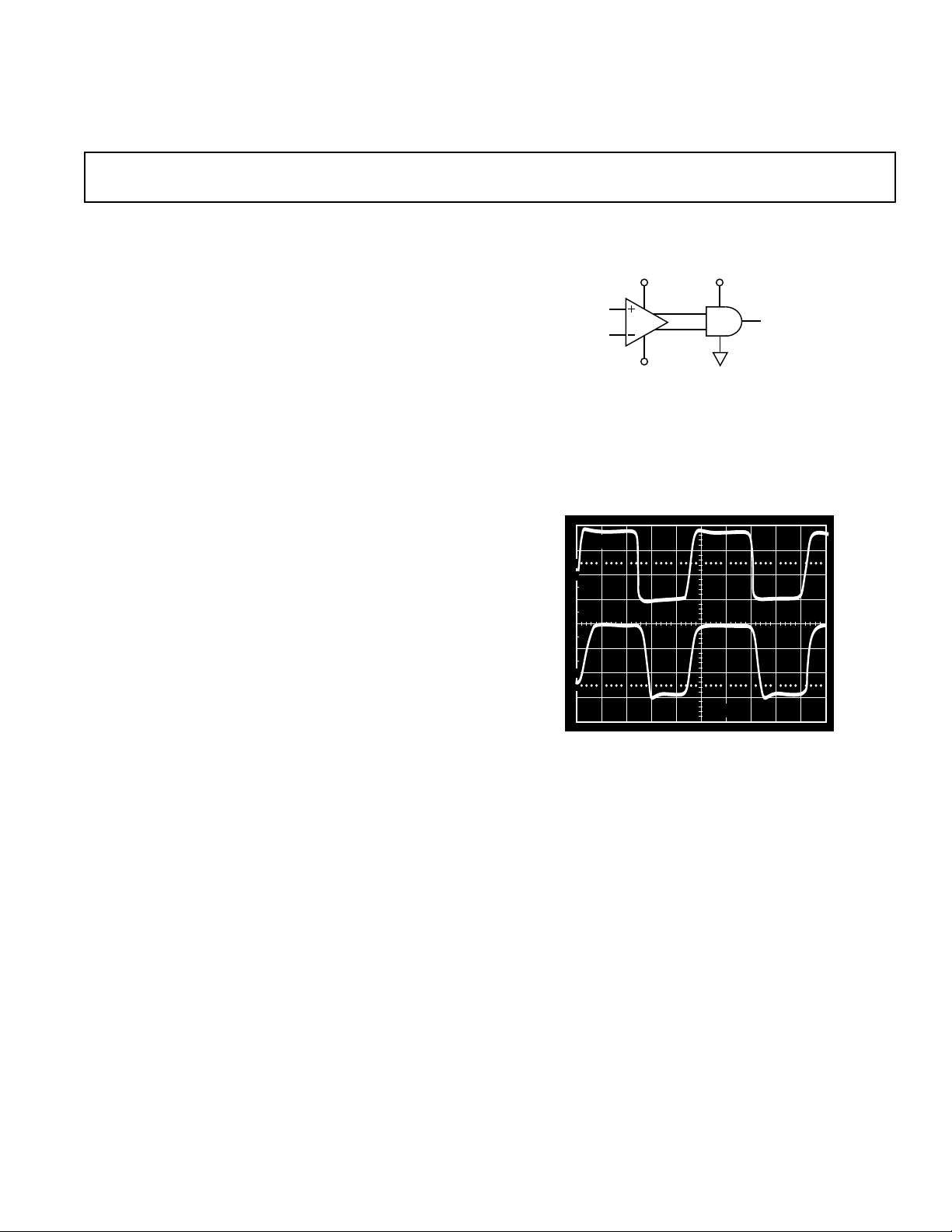
CMP401: 20 MHz Noninverting Switching. VIN = ±100 mV
© Analog Devices, Inc., 1995
One Technology Way, P.O. Box 9106, Norwood, MA 02062-9106, U.S.A.
Tel: 617/329-4700 Fax: 617/326-8703
CMP401/CMP402–SPECIFICA TIONS
ELECTRICAL SPECIFICATIONS
(@ V+
ANA
= V+
= +5.0 V, VCM = 0.1 V, –408C ≤ TA ≤ +1258C unless otherwise noted)
DIG
Parameter Symbol Conditions Min Typ Max Units
INPUT CHARACTERISTICS
Offset Voltage
Offset Voltage
1
1
V
OS
V
OS
TA = +25°C3mV
4mV
Hysteresis 2mV
Input Bias Current I
Input Offset Current I
Input Common-Mode Voltage Range V
B
I
B
OS
CM
TA = +25°C3µA
4µA
±3 µA
0 +4.0 V
Common-Mode Rejection CMRR 0.1 V ≤ VCM ≤ 3.9 V 60 dB
Large Signal Voltage Gain A
VO
RL = 10 kΩ 10 V/mV
Offset Voltage Drift ∆VOS/∆T1µV/°C
OUTPUT CHARACTERISTICS
Output High Voltage V
Output Low Voltage V
OH
OL
IOH = –3.2 mA 4.6 V
IOL = 3.2 mA 0.2 V
POWER SUPPLY
Power Supply Rejection Ratio PSRR V+
Analog Supply Current – CMP401 I
Digital Supply Current – CMP401 I
Analog Supply Current – CMP401 I
Digital Supply Current – CMP401 I
Analog Supply Current – CMP402 I
Digital Supply Current – CMP402 I
Analog Supply Current – CMP402 I
Digital Supply Current – CMP402 I
ANA
DIG
ANA
DIG
ANA
DIG
ANA
DIG
ANA
and V+
+2.7 V to +6 V 60 dB
DIG
TA = +25°C 6.5 mA
VO = 0 V, RL = ∞, TA = +25°C 2.0 mA
8.0 mA
VO = 0 V, RL = ∞ 2.25 mA
TA = +25°C 1.4 mA
VO = 0 V, RL = ∞, TA = +25°C 2.0 mA
1.75 mA
VO = 0 V, RL = ∞ 2.25 mA
DYNAMIC PERFORMANCE
Propagation Delay – CMP401 t
Propagation Delay – CMP401 t
Propagation Delay – CMP401 t
Propagation Delay – CMP402 t
P
P
P
P
100 mV Step with 20 mV OD,
T
= +25°C1723ns
A
100 mV Step with 5 mV OD,
T
= +25°C33ns
A
100 mV Step with 20 mV OD 30 ns
100 mV Step with 20 mV OD,
TA = +25°C5465ns
Propagation Delay – CMP402 t
P
100 mV Step with 5 mV OD,
TA = +25°C60ns
Propagation Delay – CMP402 t
P
100 mV Step with 20 mV OD 75 ns
ELECTRICAL SPECIFICATIONS
(@ V
ANA
= V
= +3.0 V, VCM = 0.1 V, TA = +258C unless otherwise noted)
DIG
Parameter Symbol Conditions Min Typ Max Units
INPUT CHARACTERISTICS
Offset Voltage
Input Common-Mode Voltage Range V
Input Differential Voltage Range V
Common-Mode Rejection CMRR 0.1 V ≤ V
1
V
OS
CM
DIFF
4.5 mV
0 +2.0 V
±2.0 V
≤ 1.9 V 60 dB
CM
OUTPUT CHARACTERISTICS
Output High Voltage V
Output Low Voltage V
OH
OL
IOH = –3.2 mA 2.6 V
IOL = 3.2 mA 0.25 V
POWER SUPPLY
Power Supply Rejection Ratio PSRR V+
Analog Supply Current – CMP401 I
Digital Supply Current – CMP401 I
Analog Supply Current – CMP402 I
Digital Supply Current – CMP402 I
ANA
DIG
ANA
DIG
ANA
and V+
+2.7 V to +6 V 60 dB
DIG
6mA
VO = 0 V, RL = ∞ 1mA
1.2 mA
VO = 0 V, RL = ∞ 1mA
DYNAMIC PERFORMANCE
Propagation Delay – CMP401 t
Propagation Delay – CMP402 t
P
P
100 mV Step with 20 mV OD 32 ns
100 mV Step with 20 mV OD 70 ns
–2–
REV. 0

CMP401/CMP402
ELECTRICAL SPECIFICATIONS
(@ V±
= ±5 V, V
ANA
= +5.0 V, TA = +258C unless otherwise noted)
DIG
Parameter Symbol Conditions Min Typ Max Units
INPUT CHARACTERISTICS
Offset Voltage
Input Common-Mode Voltage Range V
Input Differential Voltage Range V
1
V
OS
CM
DIFF
VCM = 0 V 3 mV
–5.0 +4.0 V
±8.0 V
Common-Mode Rejection CMRR –4.9 V ≤ VCM ≤ 3.9 V 60 dB
Offset Voltage Drift ∆VOS/∆T15µV/°C
POWER SUPPLY
Power Supply Rejection Ratio PSRR V±
Analog Supply Current – CMP401 I
Digital Supply Current – CMP401 I
Analog Supply Current – CMP402 I
Digital Supply Current – CMP402 I
ANA
DIG
ANA
DIG
±3 V to ±6 V 60 dB
ANA
6.5 mA
VO = 0 V, RL = ∞ 2.0 mA
2.0 mA
VO = 0 V, RL = ∞ 2.0 mA
DYNAMIC PERFORMANCE
Propagation Delay – CMP401 t
Propagation Delay – CMP402 t
NOTES
1
Offset voltage is defined as (V
Specifications subject to change without notice.
OS+
+ V
OS–
)/2.
P
P
100 mV Step with 20 mV OD 23 ns
100 mV Step with 20 mV OD 65 ns
REV. 0
–3–

CMP401/CMP402
WARNING!
ESD SENSITIVE DEVICE
2 1 16 15
89
3
4
5
6
7
14
13
12
11
10
+IN
–IN
V+ ANA
V– ANA
V+ DIG
OUT
DIG GND
ABSOLUTE MAXIMUM RATINGS
1
Total Analog Supply Voltage . . . . . . . . . . . . . . . . . . . . . +16 V
Digital Supply Voltage . . . . . . . . . . . . . . . . . . . . . . . . . . . +7 V
Analog Positive Supply—Digital Positive Supply . . . . –200 mV
Input Voltage
2
. . . . . . . . . . . . . . . . . . . . . . . . . . . . . . . . . ±7 V
Differential Input Voltage . . . . . . . . . . . . . . . . . . . . . . . . ±9 V
Output Short-Circuit Duration to GND . . . . . . . . . Indefinite
Storage Temperature Range
P, S, RU Package . . . . . . . . . . . . . . . . . . . –65°C to +150°C
Operating Temperature Range
CMP401G, CMP402G . . . . . . . . . . . . . . –40°C to +125°C
Junction Temperature Range
P, S, RU Package . . . . . . . . . . . . . . . . . . . –65°C to +150°C
Lead Temperature Range (Soldering, 60 sec) . . . . . . . +300°C
Package Type u
3
JA
u
JC
Units
16-Pin Plastic DIP (P) 90 47 °C/W
16-Pin SO (S) 113 37 °C/W
16-Lead TSSOP (RU) 180 37 °C/W
NOTES
1
Absolute maximum ratings apply to both DICE and packaged parts, unless
otherwise noted.
2
The analog input voltage is equal to ± 7 volts or the analog supply voltage,
whichever is less.
3
θJA is specified for the worst case conditions, i.e., θ
for P-DIP, and θ
TSSOP packages.
is specified for device soldered in circuit board for SOIC and
JA
is specified for device in socket
JA
DICE CHARACTERISTICS
CMP401/CMP402 Die Size 0.065 × 0.069 inch, 4,485 sq. mils
Substrate (Die Backside) Is Connected to V+
Transistor Count 104.
ORDERING GUIDE
Temperature Package Package
Model Range Description Option
CMP401GP –40°C to +125°C 16-Pin Plastic DIP N-16
CMP401GS –40°C to +125°C 16-Pin SOIC R-16A
CMP401GRU –40°C to +125°C 16-Lead TSSOP RU-16
CMP402GP –40°C to +125°C 16-Pin Plastic DIP N-16
CMP402GS –40°C to +125°C 16-Pin SOIC R-16A
CMP402GRU –40°C to +125°C 16-Lead TSSOP RU-16
CMP401/CMP402 PIN CONFIGURATIONS
16-Lead Epoxy DIP
16-Lead Narrow-SO
(P Suffix)
16
15
14
13
12
11
10
9
OUT C
OUT D
DIG GND
V– ANA
–IN D
+IN D
–IN C
+IN C
OUT B
OUT A
V+ DIG
V+ ANA
–IN A
+IN A
–IN B
+IN B
OUT B
OUT A
V+ DIG
V+ ANA
–IN A
+IN A
–IN B
+IN B
1
2
3
4
5
6
7
8
(S Suffix)
1
2
3
CMP401/
4
402
TOP VIEW
5
(Not to Scale)
6
7
8
16
15
14
13
12
11
10
9
OUT C
OUT D
DIG GND
V– ANA
–IN D
+IN D
–IN C
+IN C
Figure 1. Simplified Schematic
16-Lead
TSSOP
(RU Suffix)
116
OUT B
OUT A
V+ DIG
V+ ANA
–IN A
+IN A
–IN B
+IN B
CMP401/
402
TOP VIEW
(Not to Scale)
8
OUT C
OUT D
DIG GND
V– ANA
–IN D
+IN D
–IN C
+IN C
9
CAUTION
ESD (electrostatic discharge) sensitive device. Electrostatic charges as high as 4000 V readily
accumulate on the human body and test equipment and can discharge without detection.
Although the CMP401/CMP402 features proprietary ESD protection circuitry, permanent damage
may occur on devices subjected to high energy electrostatic discharges. Therefore, proper ESD
precautions are recommended to avoid performance degradation or loss of functionality.
–4–
REV. 0

T ypical Performance Characteristics–CMP401 /CMP402
TEMPERATURE – °C
PROPAGATION DELAY – ns
40
10
–50 –25 125
0 255075100
35
30
25
20
15
+P
DELAY
–P
DELAY
+VAN = +V
DIG
= +5V
–V
AN
= 0V TO –5V
R
S
≤ 50Ω, CL = 15pF
TEMPERATURE – °C
PROPAGATION DELAY – ns
60
0
–50 –25 125
0255075100
50
40
30
20
10
+VAN = +V
DIG
= +5V
–V
AN
= 0V TO –5V
R
S
≤ 50Ω, CL = 15pF
+P
DELAY
–P
DELAY
POSITIVE SUPPLY VOLTAGE – Volts
PROPAGATION DELAY – ns
80
70
0
02 6
345
40
30
20
10
60
50
+VAN = +V
DIG
–VAN = 0V TO –5V
RS ≤ 50Ω, CL = 15pF
T
A
= +25°C
+P
DELAY
–P
DELAY
40
35
30
25
20
15
10
PROPAGATION DELAY – ns
5
0
010 50
+VAN = +V
= 0V TO –5V
–V
AN
R
≤ 50Ω, CL = 15pF
S
= +25°C
T
A
+P
DELAY
–P
DELAY
20 30 40
OVERDRIVE – mV
DIG
= +5V
Figure 2. CMP401 Propagation Delay
vs. Overdrive
90
+VAN = +V
–V
AN
80
R
S
70
60
50
PROPAGATION DELAY – ns
40
30
–50 –25 125
= +5V
DIG
= 0V TO –5V
≤ 50Ω, CL = 15pF
+P
DELAY
–P
DELAY
0255075100
TEMPERATURE – °C
110
90
80
70
60
50
40
PROPAGATION DELAY – ns
30
20
010 50
+VAN = +V
–V
R
S
T
A
+P
DELAY
–P
DELAY
20 30 40
OVERDRIVE – mV
= +5V
DIG
= 0V TO –5V
AN
≤ 50Ω, CL = 15pF
= +25°C
Figure 3. CMP402 Propagation Delay
vs. Overdrive
30
25
20
15
10
PROPAGATION DELAY – ns
5
0
–50 –25 125
+P
DELAY
–P
DELAY
+VAN = +V
DIG
= 0V TO –5V
–V
AN
R
≤ 50Ω, CL = 15pF
S
0255075100
TEMPERATURE – °C
= +5V
Figure 4. CMP401 Propagation Delay
vs. Temperature – 5 mV OD
Figure 5. CMP402 Propagation Delay
vs. Temperature – 5 mV OD
90
+VAN = +V
80
–V
T
A
70
60
50
40
30
20
PROPAGATION DELAY – ns
10
0
10 100 100k
= +5V
DIG
= 0V TO –5V
AN
= +25°C
+P
DELAY
SOURCE RESISTANCE – Ω
Figure 8. CMP401 Propagation Delay
vs. Source Resistance – 20 mV OD
REV. 0
–P
DELAY
1k 10k
Figure 6. CMP401 Propagation Delay
vs. Temperature – 20 mV OD
120
+VAN = +V
–VAN = 0V TO –5V
100
TA = +25°C
80
60
40
PROPAGATION DELAY – ns
20
0
10 100 100k
= +5V
DIG
+P
DELAY
–P
DELAY
SOURCE RESISTANCE – Ω
1k 10k
Figure 9. CMP402 Propagation Delay
vs. Source Resistance – 20 mV OD
–5–
Figure 7. CMP402 Propagation Delay
vs. Temperature – 20 mV OD
Figure 10. CMP401 Propagation Delay
vs. Supply Voltage – 20 mV OD

CMP401/CMP402
CAPACITIVE LOAD – pF
PROPAGATION DELAY – ns
90
80
0
0 100 500
200 300 400
40
30
20
10
70
50
60
+VAN = +V
DIG
=
+5V
–VAN = 0V TO –5V
RS ≤ 50Ω, TA = +25°C
+P
DELAY
–P
DELAY
LOAD CURRENT – µA
1000
10
0.1
1 10 100000
100 1000 10000
100
1
DELTA OUTPUT SWING – mV
TA = +25°C
–∆RAIL
+∆RAIL
TEMPERATURE – °C
2.0
1.6
0.0
–75 –50 150
–25 0 25 75 100 12550
1.2
0.8
0.4
+5V
DIGITAL DC SUPPLY CURRENT – mA
+3V
110
100
90
80
70
60
50
PROPAGATION DELAY – ns
40
30
12 6345
POSITIVE SUPPLY VOLTAGE – Volts
–P
DELAY
+VAN = +V
DIG
–VAN = 0V TO –5V
RS ≤ 50Ω, CL = 15pF
= +25°C
T
A
+P
DELAY
Figure 11. CMP402 Propagation Delay
vs. Supply Voltage – 20 mV OD
1200
+VAN = +V
DIG
–VAN = 0V TO –5V
1000
RS ≤ 50Ω, CL = 15pF
= +25°C
T
A
800
600
400
SLEWRATE – V/µs
200
0
12 6
POSITIVE SUPPLY VOLTAGE – Volts
–SLEW
345
+SLEW
50
45
40
35
30
25
20
15
10
PROPAGATION DELAY – ns
5
0
+P
DELAY
–P
DELAY
+VAN = +V
–V
R
S
0 100 500
200 300 400
CAPACITIVE LOAD – pF
=
+5V
DIG
= 0V TO –5V
AN
= 50Ω, TA = +25°C
Figure 12. CMP401 Propagation Delay
vs. Capacitive Load
80
70
60
50
40
30
20
PROPAGATION DELAY – ns
10
0
12 6
SUPPLY VOLTAGE – Volts
+VAN = +V
DIG
–VAN = 0V TO –5V
RS ≤ 50Ω, CL = 15pF
= +25°C
T
A
+P
DELAY
–P
DELAY
345
Figure 13. CMP402 Propagation Delay
vs. Capacitive Load
Figure 14. CMP401/CMP402 Slew Rate
vs. Positive Supply Voltage
2.5
2.0
1.5
1
0.5
INPUT OFFSET VOLTAGE – mV
0
–75 –50 150–25 0 25 75 100 12550
Figure 17. CMP401/CMP402 Input
Offset Voltage vs. Temperature
TEMPERATURE – °C
Figure 15. CMP401 Propagation Delay
vs. Supply Voltage
2.0
1.6
+5V
1.2
0.8
0.4
+3V
DIGITAL DC SUPPLY CURRENT – mA
0.0
–25 0 25 75 100 12550
–75 –50 150
TEMPERATURE – °C
Figure 18. CMP401 Digital Supply
Current vs. Temperature
–6–
Figure 16. CMP401/CMP402 Delta
Output Swing from Power Supplies vs.
Load Current
Figure 19. CMP402 Digital Supply
Current vs. Temperature
REV. 0

CMP401/CMP402
TEMPERATURE – °C
ANALOG SUPPLY CURRENT – mA
7.0
6.0
2.0
–75 –50 150
–25 0 25 75 100 12550
5.0
4.0
3.0
+5V
±5V
+3V
ANALOG SUPPLY VOLTAGE – V
1.4
1.2
0.4
12 10
345 7896
1.0
0.8
0.6
ANALOG SUPPLY CURRENT – mA
+25°C
+125°C
–40°C
1.6
1.2
0.8
0.4
DIGITAL SUPPLY CURRENT – mA
0.0
15
234
DIGITAL SUPPLY VOLTAGE – V
–40°C
+25°C
+125°C
Figure 20. CMP401 Digital Supply
Current vs. Digital Supply Voltage
1.4
±5V
1.2
1.0
0.8
+5V
+3V
1.6
1.2
0.8
0.4
DIGITAL SUPPLY CURRENT – mA
0.0
15
Figure 21. CMP402 Digital Supply
Current vs. Digital Supply Voltage
7.0
6.0
5.0
4.0
234
DIGITAL SUPPLY VOLTAGE – V
–40°C
+25°C
+125°C
Figure 22. CMP401 Analog Supply
Current vs. Temperature
+125°C
+25°C
–40°C
0.6
ANALOG SUPPLY CURRENT – mA
0.4
–75 –50 150
–25 0 25 75 100 12550
TEMPERATURE – °C
Figure 23. CMP402 Analog Supply
Current vs. Temperature
3.0
ANALOG SUPPLY CURRENT – mA
2.0
345 7896
12 10
ANALOG SUPPLY VOLTAGE – V
Figure 24. CMP401 Analog Supply
Current vs. Analog Supply Voltage
Figure 25. CMP402 Analog Supply
Current vs. Analog Supply Voltage
REV. 0
–7–

CMP401/CMP402
0.210 (5.33)
MAX
0.160 (4.06)
0.115 (2.93)
OUTLINE DIMENSIONS
Dimensions shown in inches and (mm).
16-Pin Epoxy DIP
(N-16)
0.840 (21.33)
0.745 (18.93)
16
18
PIN 1
0.022 (0.558)
0.014 (0.356)
0.100
(2.54)
BSC
9
0.280 (7.11)
0.240 (6.10)
0.060 (1.52)
0.015 (0.38)
0.130
(3.30)
MIN
0.070 (1.77)
0.045 (1.15)
SEATING
PLANE
16-Pin Narrow-SOIC
(R-16A)
0.325 (8.25)
0.300 (7.62)
0.015 (0.381)
0.008 (0.204)
0.195 (4.95)
0.115 (2.93)
C2067–18–10/95
16 9
PIN 1
1
0.3937 (10.00)
0.0098 (0.25)
0.0040 (0.10)
0.006 (0.15)
0.002 (0.05)
SEATING
PLANE
0.0500 (1.27)
BSC
16 9
0.177 (4.50)
0.169 (4.30)
1
PIN 1
0.0256
(0.65)
BSC
0.3859 (9.80)
0.201 (5.10)
0.193 (4.90)
0.0118 (0.30)
0.0075 (0.19)
0.1574 (4.00)
0.1497 (3.80)
0.2440 (6.20)
8
0.2284 (5.80)
0.0688 (1.75)
0.0532 (1.35)
0.0192 (0.49)
0.0138 (0.35)
0.0099 (0.25)
0.0075 (0.19)
16-Lead TSSOP
(RU-16)
0.256 (6.50)
0.246 (6.25)
8
0.0433
(1.10)
MAX
0.0079 (0.20)
0.0035 (0.090)
8°
0°
0.0196 (0.50)
0.0099 (0.25)
8
°
0
°
0.028 (0.70)
0.020 (0.50)
x 45
0.0500 (1.27)
0.0160 (0.41)
°
PRINTED IN U.S.A.
–8–
REV. 0
 Loading...